SEMINAR PRESENTATION ON IC FABRICATION PROCESS PREPARED BY
 SOURABH JAIN(12")
SEMINAR PRESENTATION ON IC FABRICATION PROCESS PREPARED BY: VAIBHAV RAJPUT(12 BEC 102) SOURABH JAIN(12 BEC 098) GUIDED BY: Dr. USHA MEHTA

CONTENTS • PROCESS OVERVIEW • DETAILED EXPLANATION OF EACH STEP • REFERENCES

PROCESS IN THE “REAL SENSE”

HOW DO THEY DO IT ? • Si used for crystal growth is purified from Si. O 2 (sand) refining, fractional distillation and CVD. through • The raw material contains < 1 ppb impurities. Pulled crystals contain O (» 1018 cm-3) and C (» 1016 cm-3), plus any added dopants placed in the melt. • Essentially all Si wafers used for ICs today come from Czochralski grown crystals. • Polysilicon material is melted, held at close to 1417 °C, crystal seed is used to start the growth. • Pull and a single rate, melt temperature and rotation rate are all important control parameters.

CZOCHRALSKI PROCESS

HERE SIZE DO MATTER !

• <100> p-type is used for IC fabrication • Wafer: 10 cm to 30 cm (~4 to ~12 inches) and 1 mm thick.

OXIDE GROWTH • Oxidation layering -> Creates a layer of Si. O 2 for insulation. • Wet Oxidation uses water vapour and Dry Oxidation uses highpurity oxygen and hydrogen at ~1000 degrees C. • Si. O 2 growth consumes silicon, grows into the substrate. • Si. O 2 is twice the volume of Si, projects above the substrate as well.

• Etched Field Oxide Isolation • First grow field oxide and then create active regions (where transistors will be created) by etching • LOCOS (Local Oxidation of Silicon) • First define active regions and then grow the oxide layers in remaining areas

• Fabricate thin Si. O 2 layer adjacent to THICK Si. O 2 layers. • Transition from THICK to thin Si. O 2 layers fabricated WITHOUT creating sharp vertical transitions.
 is evenly")
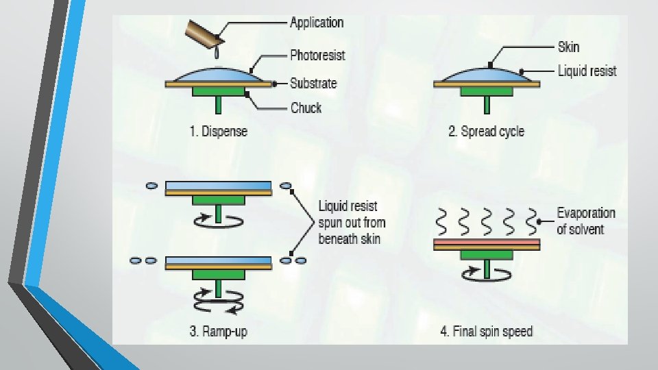
SPINNING OF ORGANIC COATING • Photoresist coating : A light-sensitive polymer (latex) is evenly spread (thickness 1 mm) by spinning the wafer. • Negative photoresist: Unexposed photoresist soluble in organic solvent, light exposure causes cross-linking making exposed regions insoluble. • Positive photoresist: Originally insoluble, exposure makes it soluble. Positive photoresist has higher resolution compared to negative resolution


n-Type Si

Si. O 2 n-Type Si

photoresist Si. O 2 n-Type Si

UV-light MASK photoresist Si. O 2 n-Type Si

• • ETCHING Wet etching • Material is selectively removed from areas that are not covered by photoresist using acids, bases and caustic solutions. • • Chemicals used here can be very dangerous to humans and the environment. Hydrofluoric acid (HF) is used for Si. O 2. Dry etching or plasma etching • • popular. • A positively charged plasma is introduced (usually a mix of nitrogen, chlorine and boron trichloride). • Rapidly moving plasma causes a chemical sandblasting action in the well defined direction of the electric field. • Clean vertical cuts can be etched using this method. Here, wafer is given a negative charge in a chamber heated to 100 degrees C under vacuum.
 • Wet etching: by chemical like HF acid (b) •")
• Sputtering (a) • Wet etching: by chemical like HF acid (b) • Dry etching : by plasma • Ion enhanced energetic (c) • Ion-enhanced-inhibitor(d)

Si. O 2 n-Type Si photoresist

photoresist Si. O 2 n-Type Si

Si. O 2 n-Type Si

THE NEXT BIG Q WHAT ARE THE METHODS OF INSERTING IMPURITY ATOMS INTO Si SUBSTARTE ? THE ANSWER IS 1)Diffusion (impurity applied at Si surface, high temperature and long time, control of doping concentration not very precise) 2)Ion implantation (impurity applied by scanning a high energy focussed ion beam at Si surface, low temperature, acceleration, precise control of doping concentration)

Si. O 2 n-Type Si p-Type BORON

n-Type Si p-Type BORON

LITHOGRAPHY TECHNIQUES

FUTURE AGENDA • 3 -D IC FABRICATION PROCESS • 3 -D PHOTOLITHOGRAPHY • CURRENT TRENDS IN FABRICATION • SOI-THE TECHNOLOGY OF FUTURE • BLOG ON HOW IT IS MADE?

REFERENCES • • • CMOS FABRICATION PROCESS BY Dr. USHA MEHTA IC FABRICATION PROCESS- INTEL CORPORATION IC FABRICATION PROCESS ANIMATION- www. ewebpal. org PHTOLITHOGRAPHY- www. movie. diginfo. tv HOW WE MAKE OUR PRODUCTS BY LEXAR HOW PROCESSORS ARE MADE FROM MICROCHIPS- www. green-translation-service. de

THANK YOU
- Slides: 29