SEMINAR PRESENTATION ON IC FABRICATION PROCESS PREPARED BY
 SOURABH JAIN(12")
SEMINAR PRESENTATION ON IC FABRICATION PROCESS PREPARED BY: VAIBHAV RAJPUT(12 BEC 102) SOURABH JAIN(12 BEC 098) GUIDED BY: Dr. USHA MEHTA

CONTENTS • A QUICK RECAP OF FIRST REVIEW • 3 D-IC FABRICATION PROCESS • REFERENCES

WHY 3 D FABRICATION? As transistors grow smaller and smaller to fit more on a wafer, the precision of equipment needed to reliably manufacture IC chips grows vastly in cost. Currently we are at a point where the cost to manufacture smaller transistors into an 2 D IC chip is not economical in any regard. Thus IC chip manufacturers have begun to produce 3 D structures on wafers allowing for more transistors per chip without the incurred cost of nanofabrication level machinery. This trade off for more transistors in the vertical as compared with the horizontal comes with both great benefits and challenges.
 ICs")
What is a 3 D IC? Could be Heterogeneous… “Stacked” 2 D (Conventional) ICs

3 D FABRICATION TECHNOLOGIES Beam Recrystallization Processed Wafer Bonding Silicon Epitaxial Growth Solid Phase Crystallization Deposit poly-silicon -not practical for 3 D circuits Bond two fully processed wafers together. -Similar Electrical Properties Epitaxially grow a single crystal Si Low Temp alternative to SE. on all devices -Independent of temp. since all chips are fabricated then bonded -Good for applications where chips do independent processing -High temperatures cause -Offers Flexibility of creating significant degradation in quality of devices on lower layers -Process not yet manufacturable. multiple layers -Compatible with current processing environments -Useful for Stacked SRAM and EEPROM cells due to high temp of melting poly-silicon -Suffers from Low carrier mobility

3 D IC FABRICATION STEP-1 : A crystalline structure such as another silicon wafer must be place on top of the first circuit level and joined through the process of plasma-activated lower temperature wafer bonding. Seeded Crystallization may also be used.

STEP-2 : Construction of the second or above layers on an IC is accomplished through a process of laser annealing. Laser annealing as opposed to more conventional methods allow for the first circuitry layer to remain at almost room temperature while the second or above layer gets hot enough to perform the needed fabrication steps. This is extremely useful as it will not negatively affect the doping concentrations of previous layers.
 IC")
Completed (2 layer) IC
 3 D fabrication allows circuit components to be located physically")
BENEFITS (power and bandwidth) 3 D fabrication allows circuit components to be located physically closer to each other. This allows circuits to operate with less power consumption and at a higher bandwidth - two qualities that are of utmost importance in today's technology (especially in memory).
 By producing layers individually and testing before combining them,")
BENEFITS (cost and material type) By producing layers individually and testing before combining them, cost can be reduced. If a layer is defective, only that portion of the circuit is discarded and not the entire unit. Furthermore, layers can be produced of different semiconductor materials to combine the benefits of various materials into the same chip
 In shifting from a planar to a volumetric structure, heat buildup inside")
CHALLENGES (Heat) In shifting from a planar to a volumetric structure, heat buildup inside becomes an issue. To mitigate this issue, heat must be considered in the design phase and kept to the outside of the structure.
 Producing the 3 D chips requires more manufacturing steps than producing 2")
CHALLENGES (Yield) Producing the 3 D chips requires more manufacturing steps than producing 2 D chips. Since some units are generally lost at each step, yield may be reduced. Contamination between layers is much more severe than standard 2 D chip contamination Alignment, imagine trying to align something in the nanometers of length. . . one mistake and it's all over Layered testing may help offset yield related issues.
 3 D chips are inherently more complex and difficult to visualize,")
CHALLENGES (Design complexity) 3 D chips are inherently more complex and difficult to visualize, and are thus more difficult to design for. 3 D CAD tools need to be developed to make the design process manageable and economic.
 Current processes state the interlevel interconnect density of 3 D circuits")
CHALLENGES (Wire density) Current processes state the interlevel interconnect density of 3 D circuits obtained by aligned bonding of pre-fabricated circuit levels is currently limited to about 10^6 wires/mm^2 With more advanced, in development, processes such as the one described above can reach well into the millions of wires/mm^2

Massive benefits are to be had from 3 D IC chips, however many challenges must be overcome to employ 3 D fabrication processes on a large scale, in more than the currently limited industries. It's likely that 3 D IC production will serve an important role in memory and cache memory based applications in the near future.

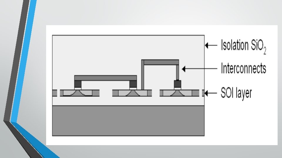
FUTURE AGENDA • CURRENT TRENDS IN FABRICATION • SOI-THE TECHNOLOGY OF FUTURE
 Rajendran, Bipin. \"Sequential 3 D IC Fabrication – Challenges and Prospects. \"")
REFERENCES 1) Rajendran, Bipin. "Sequential 3 D IC Fabrication – Challenges and Prospects. " Chomsky Stanford. Department of Electrical Engineering, Stanford University, n. d. Web. 27 Apr. 2013. <http: //chomsky. stanford. edu/data/bipin/VMIC_Rajendran_06. pdf>. 2) Patti, Robert. "Impact of Wafer-Level 3 D Stacking on the Yield of ICs. " Future Fab International. Tezzaron Semiconductor, 07 Sept. 2007. Web. 27 Apr. 2013. <http: //www. future-fab. com/documents. asp? d_ID=4415>. 3) "EDA's Big Three Unready for 3 D Chip Packaging. " EDA's Big Three Unready for 3 D Chip Packaging. EE Times, n. d. Web. 27 Apr. 2013. 4) Dally, William J. "Future Directions for On-Chip Interconnection Networks. " OCIN Workshop. 7 Dec. 2006. Web.

THANK YOU
- Slides: 19