Semikron Hong Kong Gate Driver Requirement IGBT Gate
Semikron Hong Kong Gate Driver Requirement IGBT Gate Driver Calculation Norbert Pluschke 07. 10. 2005 1

for an IGBT driver ? Gate Peak current Norbert Pluschke 07. 10. 2005 Semikron Hong Kong What is the most important requirement 2
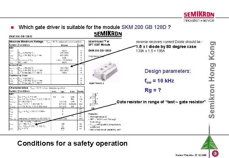
Which gate driver is suitable for the module SKM 200 GB 128 D ? reverse recovery current Diode should be - 1. 5 x I diode by 80 degree case 130 A x 1. 5 = 195 A Design parameters: fsw = 10 k. Hz Rg = ? Gate resistor in range of “test – gate resistor” Semikron Hong Kong n Conditions for a safety operation Norbert Pluschke 07. 10. 2005 3
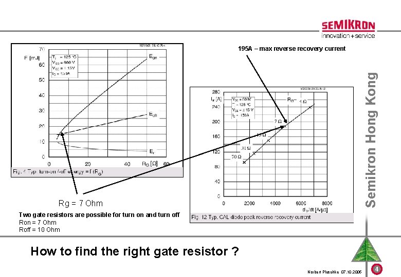
Semikron Hong Kong 195 A – max reverse recovery current Rg = 7 Ohm Two gate resistors are possible for turn on and turn off Ron = 7 Ohm Roff = 10 Ohm How to find the right gate resistor ? Norbert Pluschke 07. 10. 2005 4
n Trench Technology needs a smaller Gate charge n SPT Technology needs more Gate charge compared to Trench Technology u Driver has to provide a higher Gate charge Semikron Hong Kong u Driver has to provide a smaller Gate charge Difference between Trench- and SPT Technology Norbert Pluschke 07. 10. 2005 5
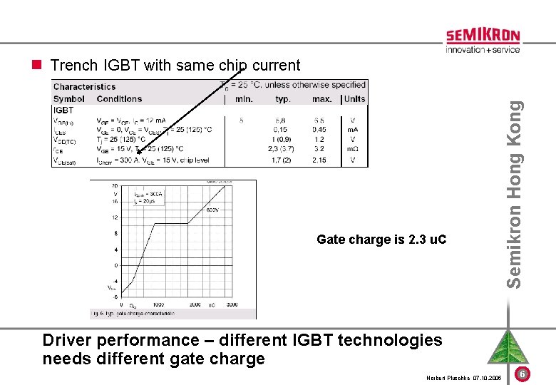
Gate charge is 2. 3 u. C Semikron Hong Kong n Trench IGBT with same chip current Driver performance – different IGBT technologies needs different gate charge Norbert Pluschke 07. 10. 2005 6
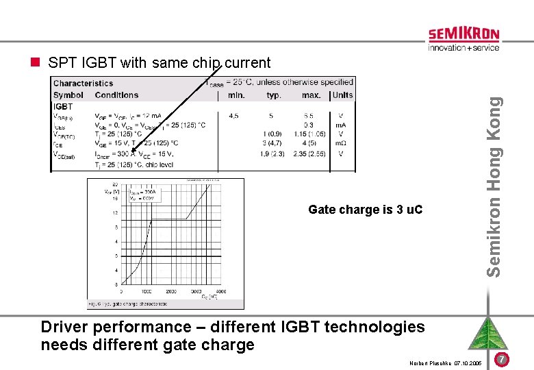
Gate charge is 3 u. C Semikron Hong Kong n SPT IGBT with same chip current Driver performance – different IGBT technologies needs different gate charge Norbert Pluschke 07. 10. 2005 7
n The suitable gate driver must provide the required è Gate charge (QG) – power supply of the driver must provide the average power è Average current (Iout. AV) – power supply è Gate pulse current (Ig. pulse) – most important Semikron Hong Kong n at the applied switching frequency (fsw) Demands for the gate driver Norbert Pluschke 07. 10. 2005 8
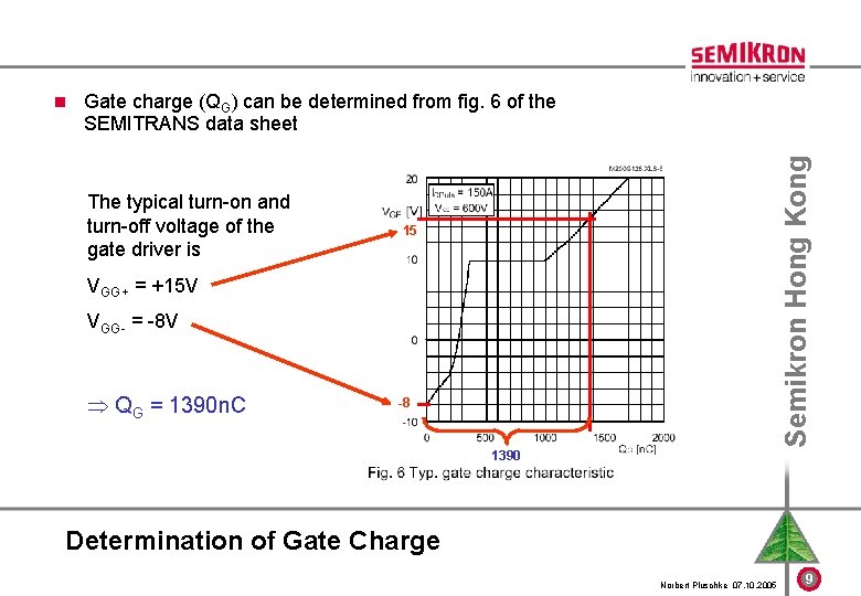
Gate charge (QG) can be determined from fig. 6 of the SEMITRANS data sheet The typical turn-on and turn-off voltage of the gate driver is Semikron Hong Kong n 15 VGG+ = +15 V VGG- = -8 V QG = 1390 n. C -8 1390 Determination of Gate Charge Norbert Pluschke 07. 10. 2005 9
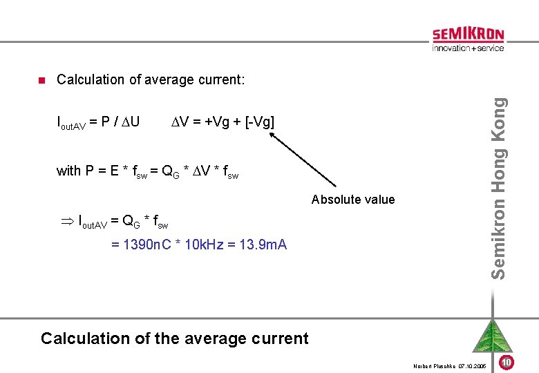
Calculation of average current: n Iout. AV = P / U n with P = E * fsw = QG * V * fsw Semikron Hong Kong n V = +Vg + [-Vg] Absolute value n Iout. AV = QG * fsw = 1390 n. C * 10 k. Hz = 13. 9 m. A Calculation of the average current Norbert Pluschke 07. 10. 2005 10
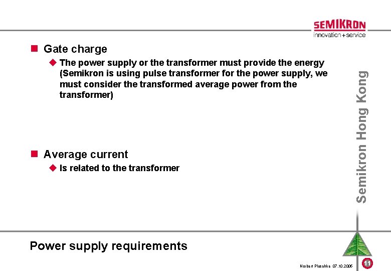
u The power supply or the transformer must provide the energy (Semikron is using pulse transformer for the power supply, we must consider the transformed average power from the transformer) n Average current u Is related to the transformer Semikron Hong Kong n Gate charge Power supply requirements Norbert Pluschke 07. 10. 2005 11
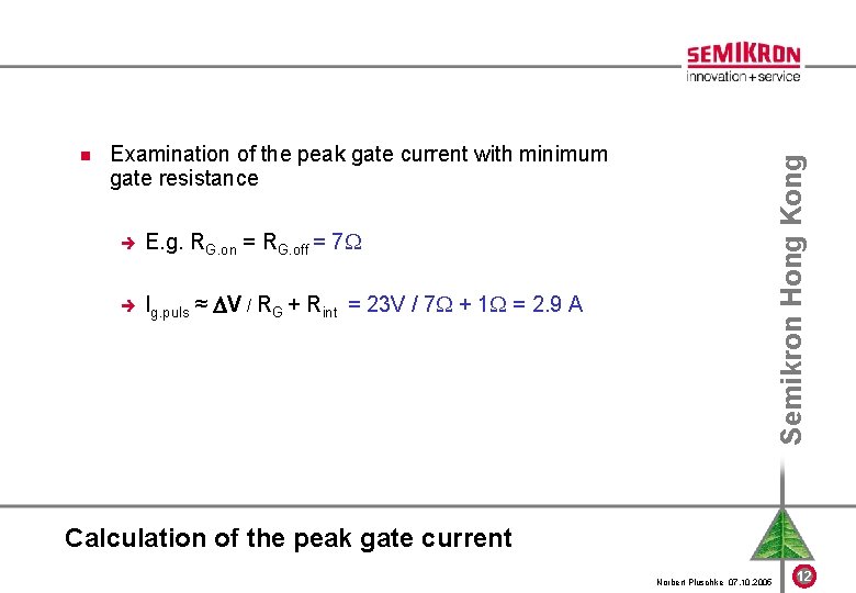
Examination of the peak gate current with minimum gate resistance è Semikron Hong Kong n E. g. RG. on = RG. off = 7 è Ig. puls ≈ V / RG + Rint = 23 V / 7 + 1 = 2. 9 A Calculation of the peak gate current Norbert Pluschke 07. 10. 2005 12
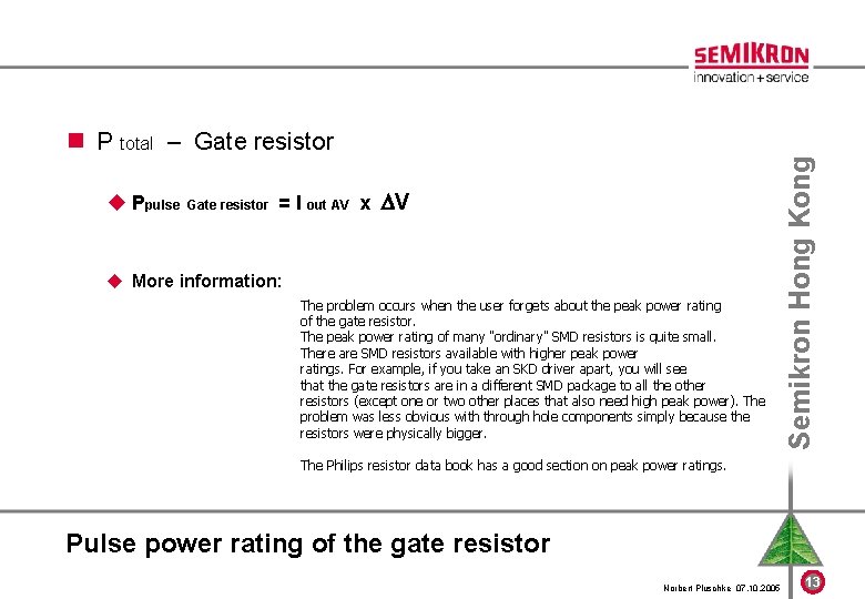
u Ppulse Gate resistor = I out AV x V u More information: The problem occurs when the user forgets about the peak power rating of the gate resistor. The peak power rating of many "ordinary" SMD resistors is quite small. There are SMD resistors available with higher peak power ratings. For example, if you take an SKD driver apart, you will see that the gate resistors are in a different SMD package to all the other resistors (except one or two other places that also need high peak power). The problem was less obvious with through hole components simply because the resistors were physically bigger. Semikron Hong Kong n P total – Gate resistor The Philips resistor data book has a good section on peak power ratings. Pulse power rating of the gate resistor Norbert Pluschke 07. 10. 2005 13
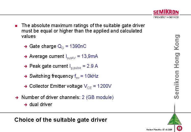
è The absolute maximum ratings of the suitable gate driver must be equal or higher than the applied and calculated values è Gate charge QG = 1390 n. C è Average current Iout. AV = 13, 9 m. A è Peak gate current Ig. pulse = 2. 9 A è Switching frequency fsw = 10 k. Hz è Collector Emitter voltage VCE = 1200 V Semikron Hong Kong n Number of driver channels: 2 (GB module) è dual driver Choice of the suitable gate driver Norbert Pluschke 07. 10. 2005 14
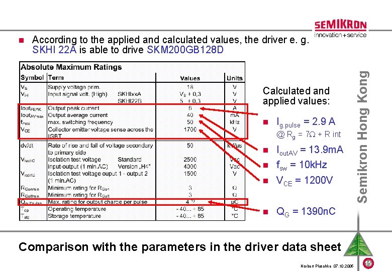
According to the applied and calculated values, the driver e. g. SKHI 22 A is able to drive SKM 200 GB 128 D Calculated and applied values: n Ig. pulse = 2. 9 A @ Rg = 7 + R int n Iout. AV = 13. 9 m. A n fsw = 10 k. Hz n VCE = 1200 V n QG = 1390 n. C Semikron Hong Kong n Comparison with the parameters in the driver data sheet Norbert Pluschke 07. 10. 2005 15
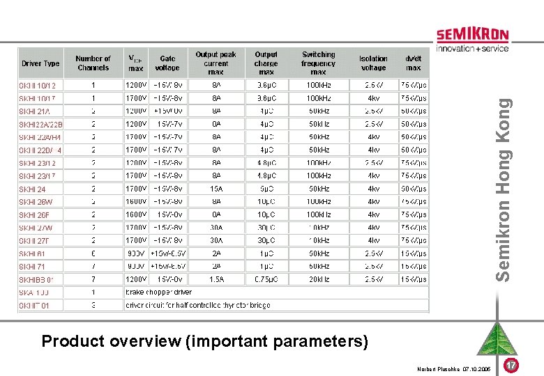
Semikron Hong Kong Product overview (important parameters) Norbert Pluschke 07. 10. 2005 17

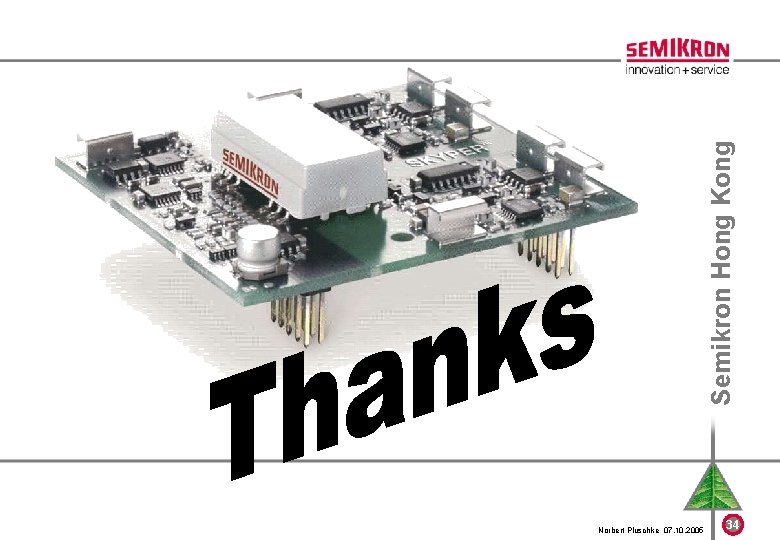
ü Adaptable ü Expandable ü Short time to market ü Two versions Ø SKYPER™ (standard version) Ø SKYPER™ PRO (premium version) Semikron Hong Kong ü Simple Driver core for IGBT modules Norbert Pluschke 07. 10. 2005 18

n Driver board n SEMIX 3 IGBT half bridge with spring contacts Semikron Hong Kong n SKYPER Assembly on SEMi. XTM 3 – Modular IPM Norbert Pluschke 07. 10. 2005 19
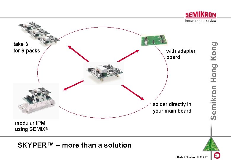
with adapter board solder directly in your main board modular IPM using SEMi. X® Semikron Hong Kong take 3 for 6 -packs SKYPER™ – more than a solution Norbert Pluschke 07. 10. 2005 20

Advice Norbert Pluschke 07. 10. 2005 Semikron Hong Kong Selection of the right IGBT driver 21
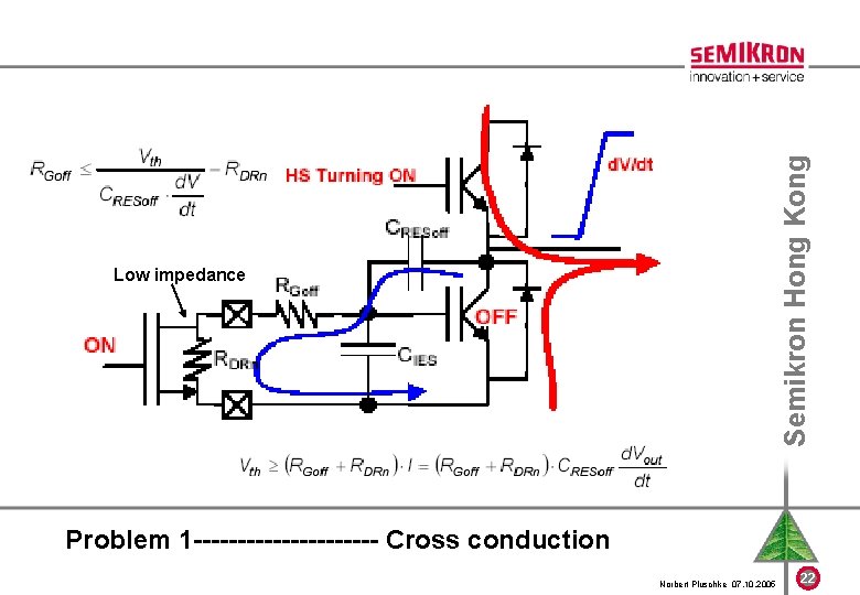
Semikron Hong Kong Low impedance Problem 1 ----------- Cross conduction Norbert Pluschke 07. 10. 2005 22
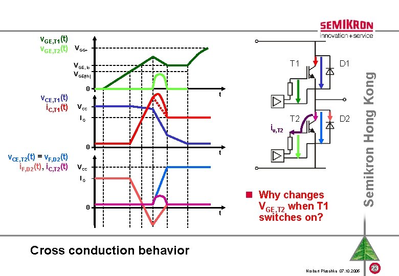
VGG+ VGE, Io VGE(th) 0 v. CE, T 1(t) i. C, T 1(t) D 1 T 2 D 2 t VCC IO iv, T 2 0 v. CE, T 2(t) = v. F, D 2(t) i. F, D 2(t), i. C, T 2(t) T 1 t VCC IO 0 t n Why changes VGE, T 2 when T 1 switches on? Semikron Hong Kong v. GE, T 1(t) v. GE, T 2(t) Cross conduction behavior Norbert Pluschke 07. 10. 2005 23
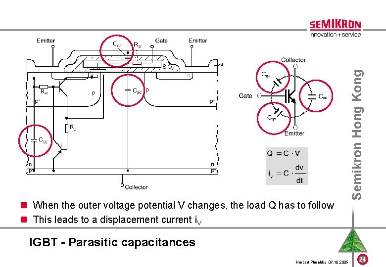
Semikron Hong Kong n When the outer voltage potential V changes, the load Q has to follow n This leads to a displacement current i. V IGBT - Parasitic capacitances Norbert Pluschke 07. 10. 2005 24
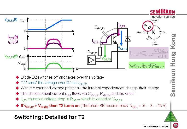
v. CE, T 2(t) VCC i. C, T 2(t) iv, T 2(t) i. C, T 2 t iv, T 2 0 t v. GE, T 2(t) VGG+ v. CE, T 2 RGE, T 2 v. GE, T 2 VGE(th) 0 u u u t Diode D 2 switches off and takes over the voltage T 2 “sees” the voltage over D 2 as v. CE, T 2 With the changed voltage potential, the internal capacitances change their charge The displacement current iv, T 2 flows via CGC, T 2, RGE, T 2 and the driver iv, T 2 causes a voltage drop in RGE, T 2 which is added to VGE, T 2 Semikron Hong Kong 0 CGC, T 2 u If v. GE, T 2 > VGE(th) then T 2 turns on (Therefore SK recommends: VGG- = -5…-8…-15 V) Switching: Detailed for T 2 Norbert Pluschke 07. 10. 2005 25
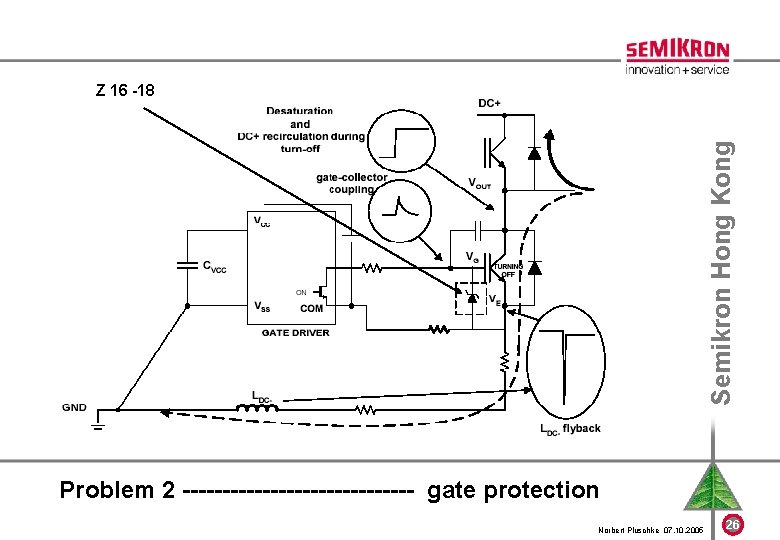
Semikron Hong Kong Z 16 -18 Problem 2 --------------- gate protection Norbert Pluschke 07. 10. 2005 26
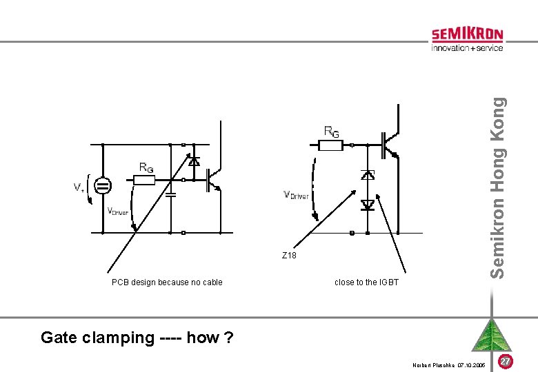
Semikron Hong Kong Z 18 PCB design because no cable close to the IGBT Gate clamping ---- how ? Norbert Pluschke 07. 10. 2005 27
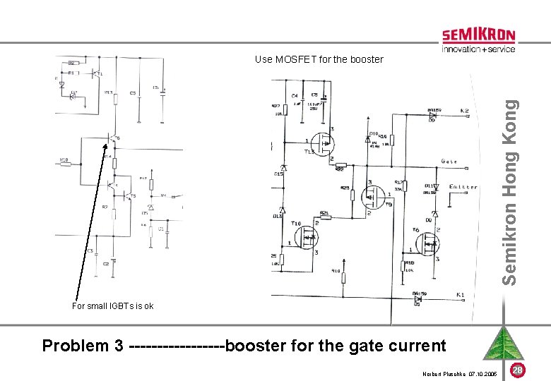
Semikron Hong Kong Use MOSFET for the booster For small IGBTs is ok Problem 3 ---------booster for the gate current Norbert Pluschke 07. 10. 2005 28
u 1200 V ----- is chip level ---- consider internal stray inductance u +/- 20 V----- gate emitter voltage ---- consider switching behavior of freewheeling diode n Over current u Power dissipation of IGBT (short circuit current x time) u Chip temperature level Semikron Hong Kong n Over voltage Problem 4 -------------- Short circuit Norbert Pluschke 07. 10. 2005 29
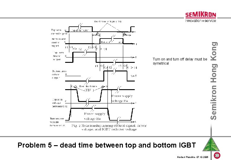
Semikron Hong Kong Turn on and turn off delay must be symetrical Problem 5 – dead time between top and bottom IGBT Norbert Pluschke 07. 10. 2005 30
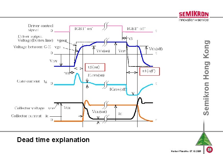
Semikron Hong Kong Dead time explanation Norbert Pluschke 07. 10. 2005 31
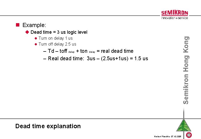
n Example: u Dead time = 3 us logic level Semikron Hong Kong l Turn on delay 1 us l Turn off delay 2. 5 us – Td – toff delay + ton delay = real dead time – Real dead time: 3 us – (2. 5 us+1 us) = 1. 5 us Dead time explanation Norbert Pluschke 07. 10. 2005 32
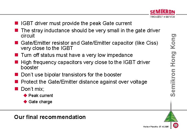
u Peak current u Gate charge Semikron Hong Kong n IGBT driver must provide the peak Gate current n The stray inductance should be very small in the gate driver circuit n Gate/Emitter resistor and Gate/Emitter capacitor (like Ciss) very close to the IGBT n Turn off status must have a very low impedance n High frequency capacitors very close to the IGBT driver booster n Don’t use bipolar transistors for the booster n Protect the Gate/Emitter distance against over voltage n Don’t mix; Our final recommendation Norbert Pluschke 07. 10. 2005 33
Semikron Hong Kong Norbert Pluschke 07. 10. 2005 34
- Slides: 33