Semiconductors Pulse shape and rise time Lecture 9
- Slides: 8

Semiconductors Pulse shape and rise time Lecture 9

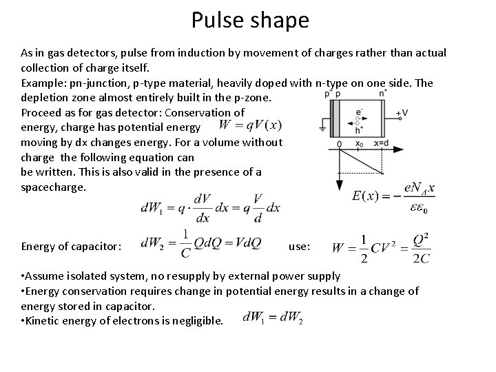
Pulse shape As in gas detectors, pulse from induction by movement of charges rather than actual collection of charge itself. Example: pn-junction, p-type material, heavily doped with n-type on one side. The depletion zone almost entirely built in the p-zone. Proceed as for gas detector: Conservation of energy, charge has potential energy moving by dx changes energy. For a volume without charge the following equation can be written. This is also valid in the presence of a spacecharge. Energy of capacitor: use: • Assume isolated system, no resupply by external power supply • Energy conservation requires change in potential energy results in a change of energy stored in capacitor. • Kinetic energy of electrons is negligible.

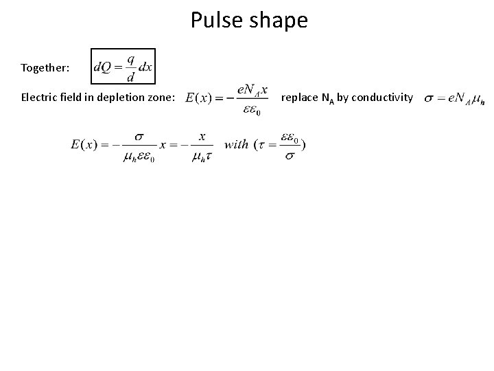
Pulse shape Together: Electric field in depletion zone: replace NA by conductivity

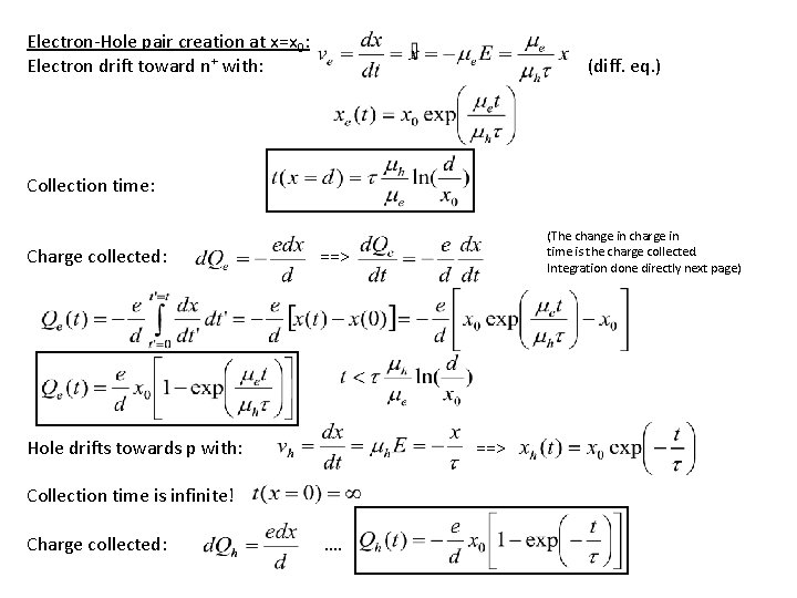
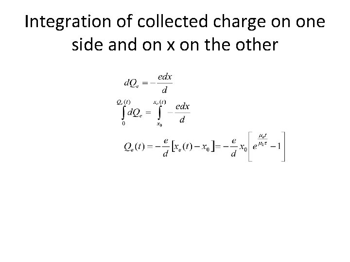
Electron-Hole pair creation at x=x 0: Electron drift toward n+ with: (diff. eq. ) Collection time: Charge collected: ==> Hole drifts towards p with: ==> Collection time is infinite! Charge collected: (The change in charge in time is the charge collected. Integration done directly next page) ….

Integration of collected charge on one side and on x on the other

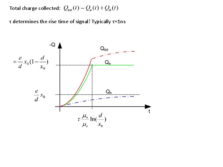
Total charge collected: τ determines the rise time of signal! Typically τ≈1 ns

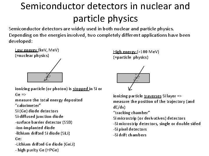
Semiconductor detectors in nuclear and particle physics Semiconductor detectors are widely used in both nuclear and particle physics. Depending on the energies involved, two completely different applications have been developed: Low energy (ke. V, Me. V) (≈nuclear physics) ionizing particle (or photon) is stopped in Si or Ge => measure the total energy deposited “calorimeter” Si (Ge) diode detectors Si-diffused junction diode -surface barrier detector (SSB) -ion-implanted diode -lithium drifted Si diode (Si. Li) Ge: -Lithium drifted Ge diode (Ge. Li) - high purity Ge (HPGe) High energy (>100 Me. V) (≈particle physics) ionizing particle traverses Si layer => measure the position of the trajectory (and d. E/dx) “tracking chamber” Si microstrip (or derivatives) detectors -Si microstrip detectors, single or double sided -Si pixel detectors -Si drift chambers

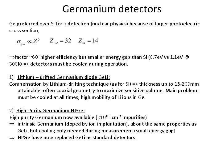
Germanium detectors Ge preferred over Si for γ detection (nuclear physics) because of larger photoelectric cross section, Þfactor ~60 higher efficiency but smaller energy gap than Si (0. 7 e. V vs 1. 1 e. V @ 300 K) => detectors must be cooled during operation. 1) Lithium – drifted Germanium diode Ge. Li: Compensation by Lithium-drifting technique (as for Si) => thickness up to 15 -200 mm attainable, often coaxial geometry to maximize sensitive volume. Main problem: must be cooled at all times, high mobility of Li ions in Ge. 2) High-Purity Germanium HPGe: High purity Germanium now available (<1010 cm-3 impurities) Þ intrinsic Germanium (doped by ion implantation), about the same properties as Ge. Li, but cooling only needed during measurement (small energy gap) Þ HPGe have now replaced Ge. Li as standard detectors.