
SEMICONDUCTORS DR A ANBARASI This Photo by Unknown
SEMICONDUCTORS DR. A. ANBARASI, This Photo by Unknown Author is licensed under CC BY-SA ASSOCIATE PROFESSOR IN PHYSICS PERIYAR ARTS COLLEGE, CUDDALORE.
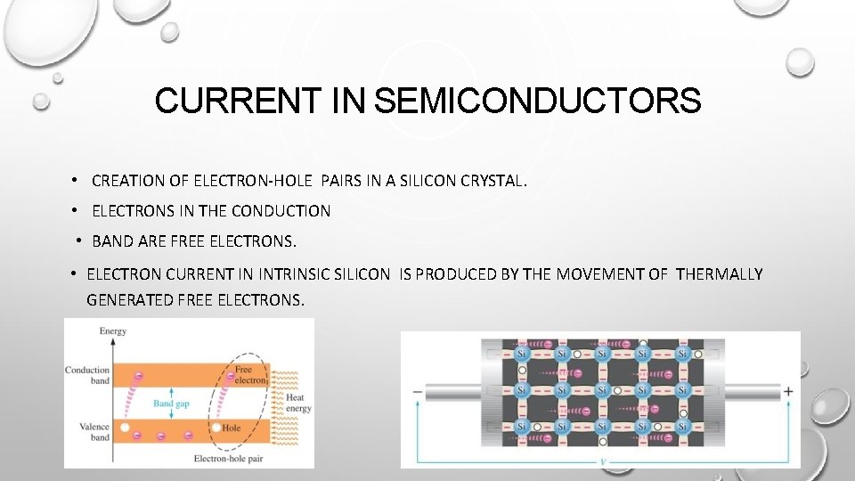
CURRENT IN SEMICONDUCTORS • CREATION OF ELECTRON-HOLE PAIRS IN A SILICON CRYSTAL. • ELECTRONS IN THE CONDUCTION • BAND ARE FREE ELECTRONS. • ELECTRON CURRENT IN INTRINSIC SILICON IS PRODUCED BY THE MOVEMENT OF THERMALLY GENERATED FREE ELECTRONS.
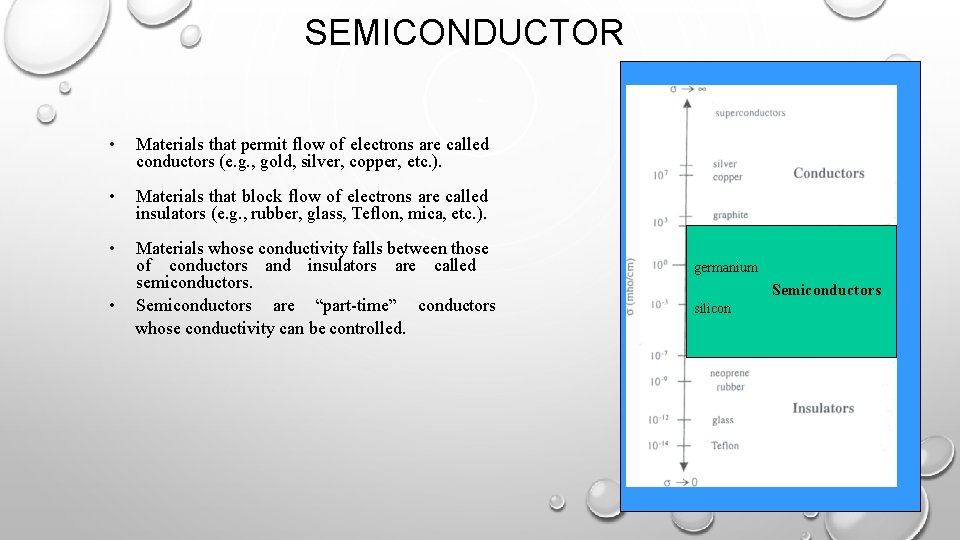
SEMICONDUCTOR • Materials that permit flow of electrons are called conductors (e. g. , gold, silver, copper, etc. ). • Materials that block flow of electrons are called insulators (e. g. , rubber, glass, Teflon, mica, etc. ). • Materials whose conductivity falls between those of conductors and insulators are called semiconductors. Semiconductors are “part-time” conductors whose conductivity can be controlled. • germanium Semiconductors silicon
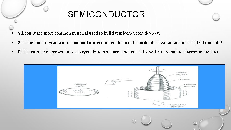
SEMICONDUCTOR • Silicon is the most common material used to build semiconductor devices. • Si is the main ingredient of sand it is estimated that a cubic mile of seawater contains 15, 000 tons of Si. • Si is spun and grown into a crystalline structure and cut into wafers to make electronic devices.
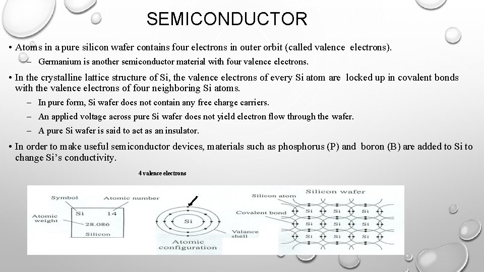
SEMICONDUCTOR • Atoms in a pure silicon wafer contains four electrons in outer orbit (called valence electrons). – Germanium is another semiconductor material with four valence electrons. • In the crystalline lattice structure of Si, the valence electrons of every Si atom are locked up in covalent bonds with the valence electrons of four neighboring Si atoms. – In pure form, Si wafer does not contain any free charge carriers. – An applied voltage across pure Si wafer does not yield electron flow through the wafer. – A pure Si wafer is said to act as an insulator. • In order to make useful semiconductor devices, materials such as phosphorus (P) and boron (B) are added to Si to change Si’s conductivity. 4 valence electrons
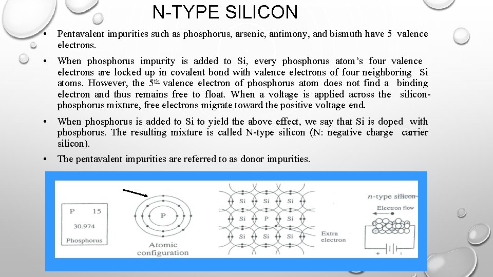
N-TYPE SILICON • Pentavalent impurities such as phosphorus, arsenic, antimony, and bismuth have 5 valence electrons. • When phosphorus impurity is added to Si, every phosphorus atom’s four valence electrons are locked up in covalent bond with valence electrons of four neighboring Si atoms. However, the 5 th valence electron of phosphorus atom does not find a binding electron and thus remains free to float. When a voltage is applied across the siliconphosphorus mixture, free electrons migrate toward the positive voltage end. • When phosphorus is added to Si to yield the above effect, we say that Si is doped with phosphorus. The resulting mixture is called N-type silicon (N: negative charge carrier silicon). • The pentavalent impurities are referred to as donor impurities.
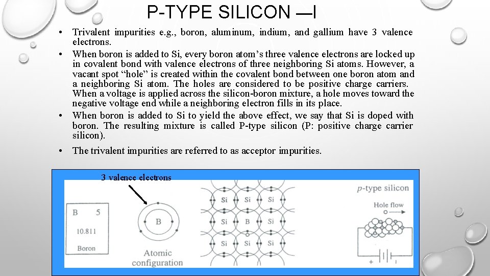
P-TYPE SILICON —I • Trivalent impurities e. g. , boron, aluminum, indium, and gallium have 3 valence electrons. • When boron is added to Si, every boron atom’s three valence electrons are locked up in covalent bond with valence electrons of three neighboring Si atoms. However, a vacant spot “hole” is created within the covalent bond between one boron atom and a neighboring Si atom. The holes are considered to be positive charge carriers. When a voltage is applied across the silicon-boron mixture, a hole moves toward the negative voltage end while a neighboring electron fills in its place. • When boron is added to Si to yield the above effect, we say that Si is doped with boron. The resulting mixture is called P-type silicon (P: positive charge carrier silicon). • The trivalent impurities are referred to as acceptor impurities. 3 valence electrons
P-TYPE SILICON — II • The hole of boron atom points towards the negative terminal. • The electron of neighboring silicon atom points toward positive terminal. • The electron from neighboring silicon atom falls into the boron atom filling the hole in boron atom and creating a “new” hole in the silicon atom. • It appears as though a hole moves toward the negative terminal!
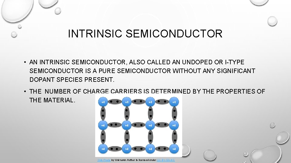
INTRINSIC SEMICONDUCTOR • AN INTRINSIC SEMICONDUCTOR, ALSO CALLED AN UNDOPED OR I-TYPE SEMICONDUCTOR IS A PURE SEMICONDUCTOR WITHOUT ANY SIGNIFICANT DOPANT SPECIES PRESENT. • THE NUMBER OF CHARGE CARRIERS IS DETERMINED BY THE PROPERTIES OF THE MATERIAL. This Photo by Unknown Author is licensed under CC BY-SA-NC
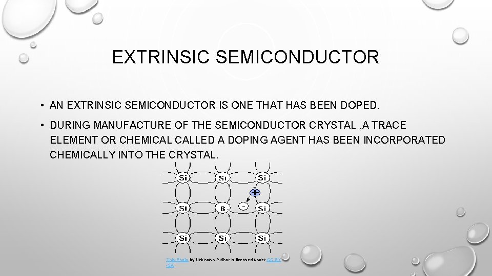
EXTRINSIC SEMICONDUCTOR • AN EXTRINSIC SEMICONDUCTOR IS ONE THAT HAS BEEN DOPED. • DURING MANUFACTURE OF THE SEMICONDUCTOR CRYSTAL , A TRACE ELEMENT OR CHEMICAL CALLED A DOPING AGENT HAS BEEN INCORPORATED CHEMICALLY INTO THE CRYSTAL. This Photo by Unknown Author is licensed under CC BY -SA
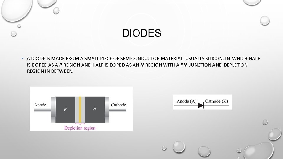
DIODES • A DIODE IS MADE FROM A SMALL PIECE OF SEMICONDUCTOR MATERIAL, USUALLY SILICON, IN WHICH HALF IS DOPED AS A P REGION AND HALF IS DOPED AS AN N REGION WITH A PN JUNCTION AND DEPLETION REGION IN BETWEEN.

DIODE PACKAGES
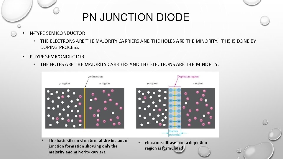
PN JUNCTION DIODE • N-TYPE SEMICONDUCTOR • THE ELECTRONS ARE THE MAJORITY CARRIERS AND THE HOLES ARE THE MINORITY. THIS IS DONE BY DOPING PROCESS. • P-TYPE SEMICONDUCTOR • THE HOLES ARE THE MAJORITY CARRIERS AND THE ELECTRONS ARE THE MINORITY. • The basic silicon structure at the instant of junction formation showing only the majority and minority carriers. • electrons diffuse and a depletion region is formulated.
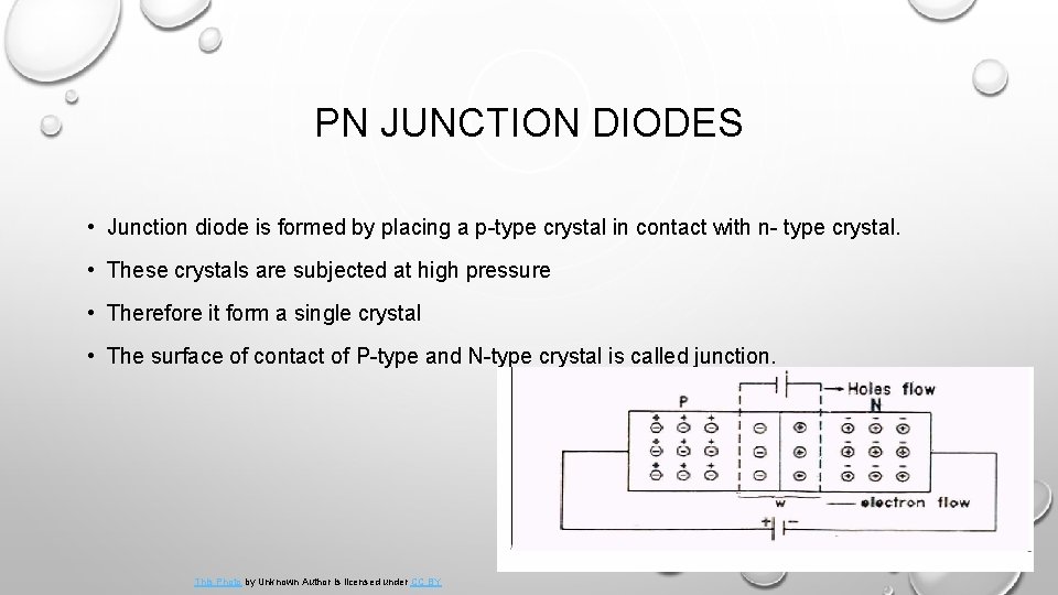
PN JUNCTION DIODES • Junction diode is formed by placing a p-type crystal in contact with n- type crystal. • These crystals are subjected at high pressure • Therefore it form a single crystal • The surface of contact of P-type and N-type crystal is called junction. This Photo by Unknown Author is licensed under CC BY
• Majority charge carriers, there is few minority charge carriers in each region • P region contain few electrons while the n-region contains a few holes • At the junction there is decreasing hole concentration from left to right • Holes diffuse from p-side to n-side • Electron diffuse from n-side to p-side • Holes leaving and electrons entering the p-side make it negative • Holes entering and electron leaving the n-side make it positive • It produces an electric field
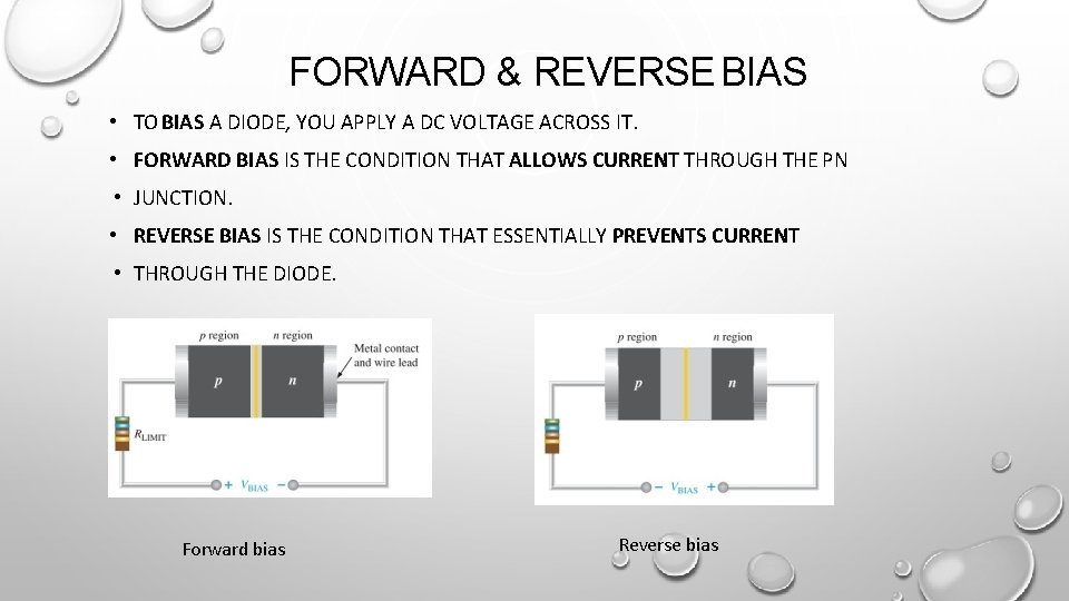
FORWARD & REVERSE BIAS • TO BIAS A DIODE, YOU APPLY A DC VOLTAGE ACROSS IT. • FORWARD BIAS IS THE CONDITION THAT ALLOWS CURRENT THROUGH THE PN • JUNCTION. • REVERSE BIAS IS THE CONDITION THAT ESSENTIALLY PREVENTS CURRENT • THROUGH THE DIODE. Forward bias Reverse bias
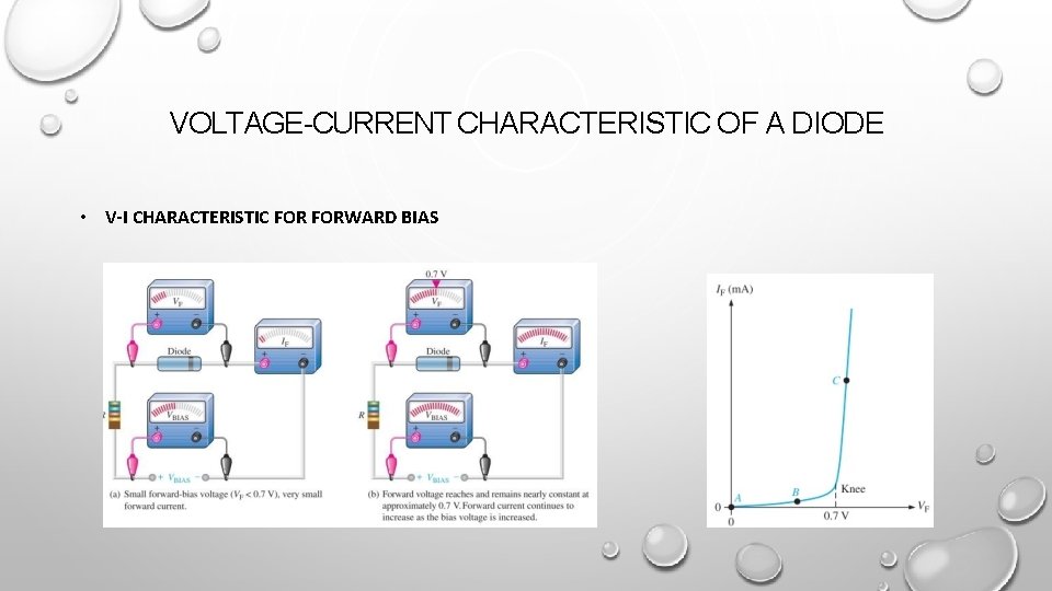
VOLTAGE-CURRENT CHARACTERISTIC OF A DIODE • V-I CHARACTERISTIC FORWARD BIAS
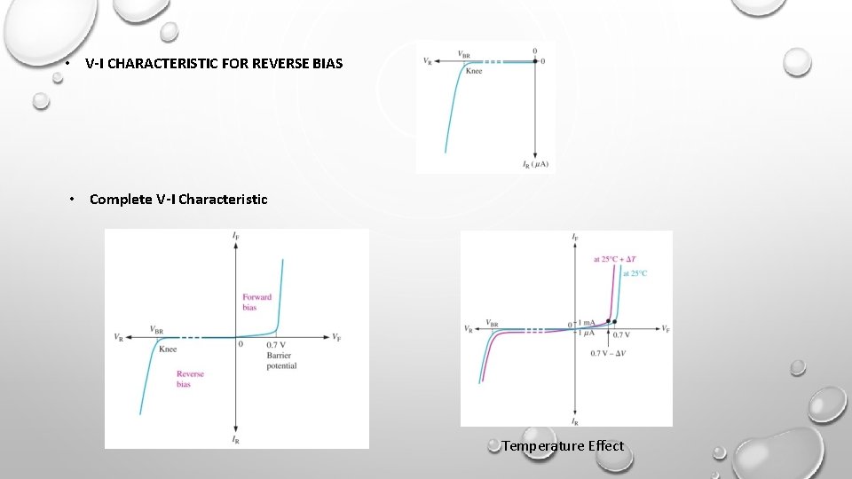
• V-I CHARACTERISTIC FOR REVERSE BIAS • Complete V-I Characteristic Temperature Effect
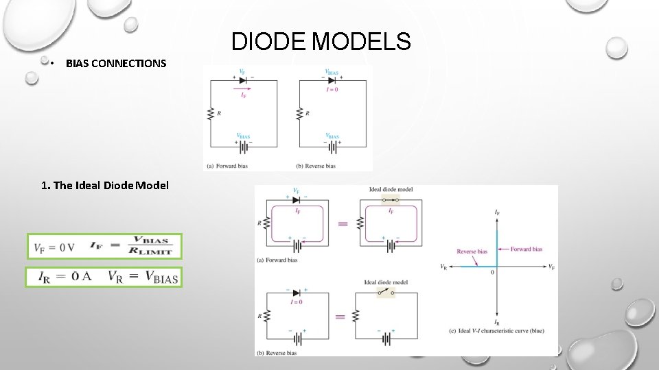
DIODE MODELS • BIAS CONNECTIONS 1. The Ideal Diode Model
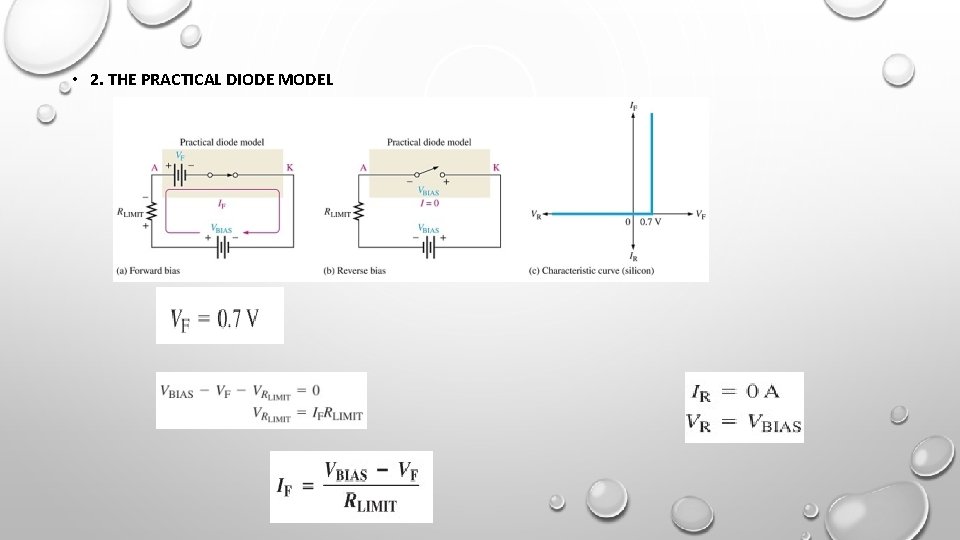
• 2. THE PRACTICAL DIODE MODEL
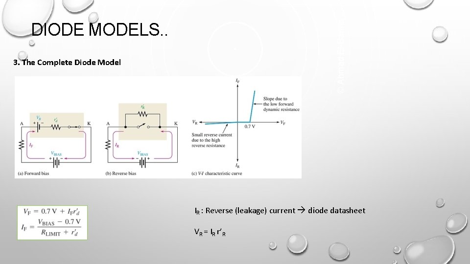
© Ahmad El-Banna DIODE MODELS. . 3. The Complete Diode Model IR : Reverse (leakage) current diode datasheet VR = IR r’R

NK YOU
- Slides: 22