Semiconductors Chapter 25 What is a Semiconductor A
- Slides: 30

Semiconductors Chapter 25

What is a Semiconductor? A Semiconductor is a substance that has a resistivity between that of a good conductor and an insulator. The resistivity of a semiconductor decreases as its temperature increases. Silicon and Germanium are semiconductors. . .

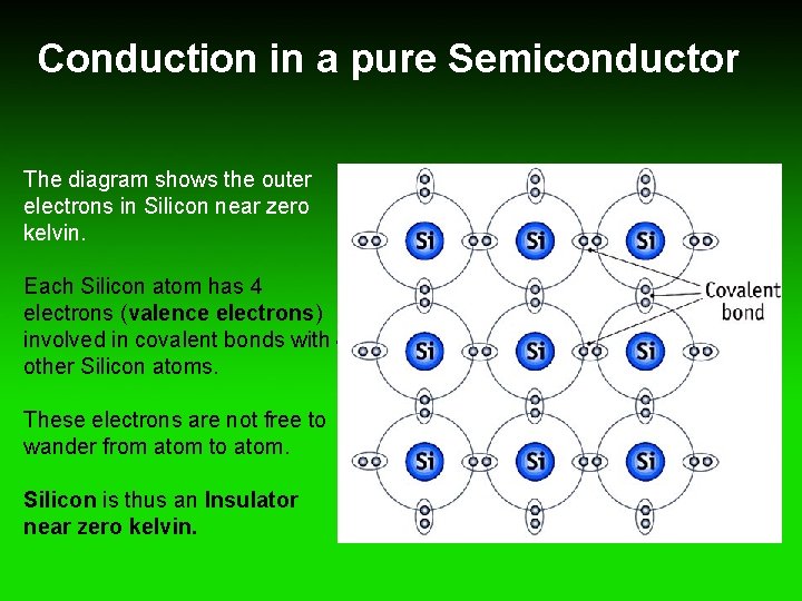
Conduction in a pure Semiconductor The diagram shows the outer electrons in Silicon near zero kelvin. Each Silicon atom has 4 electrons (valence electrons) involved in covalent bonds with 4 other Silicon atoms. These electrons are not free to wander from atom to atom. Silicon is thus an Insulator near zero kelvin.

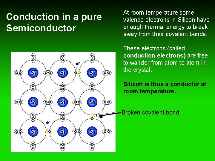
Conduction in a pure Semiconductor At room temperature some valence electrons in Silicon have enough thermal energy to break away from their covalent bonds. These electrons (called conduction electrons) are free to wander from atom to atom in the crystal. Silicon is thus a conductor at room temperature. Broken covalent bond

What are Positive Holes? When an electron breaks free from a covalent bond, it leaves behind a gap in the atom from which it came. This gap is called a Positive Hole or simply a Hole.

What is Intrinsic Conduction? Conduction in a pure semiconductor due to electrons moving from negative to positive ( - to + ) and an equal number of holes moving in the opposite direction is called Intrinsic conduction. The semiconductor is called an intrinsic semiconductor.

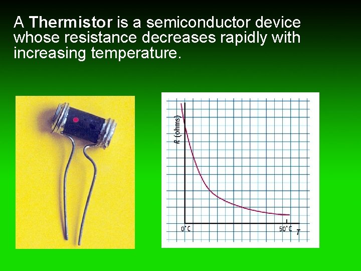
A Thermistor is a semiconductor device whose resistance decreases rapidly with increasing temperature.

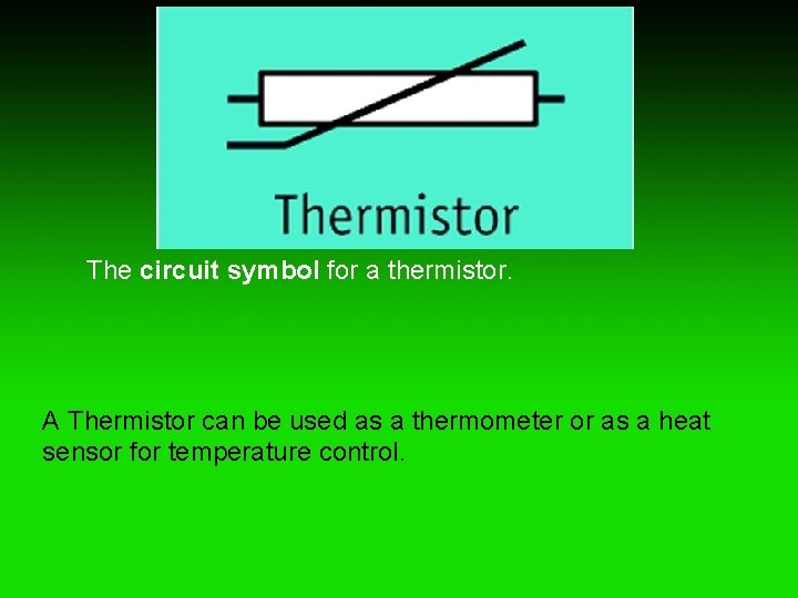
The circuit symbol for a thermistor. A Thermistor can be used as a thermometer or as a heat sensor for temperature control.

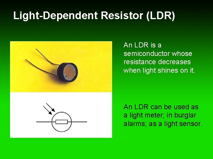
Light-Dependent Resistor (LDR) An LDR is a semiconductor whose resistance decreases when light shines on it. An LDR can be used as a light meter; in burglar alarms; as a light sensor.

What is meant by Doping? Adding a controlled amount of an impurity to a pure semiconductor to increase its conductivity is called Doping.

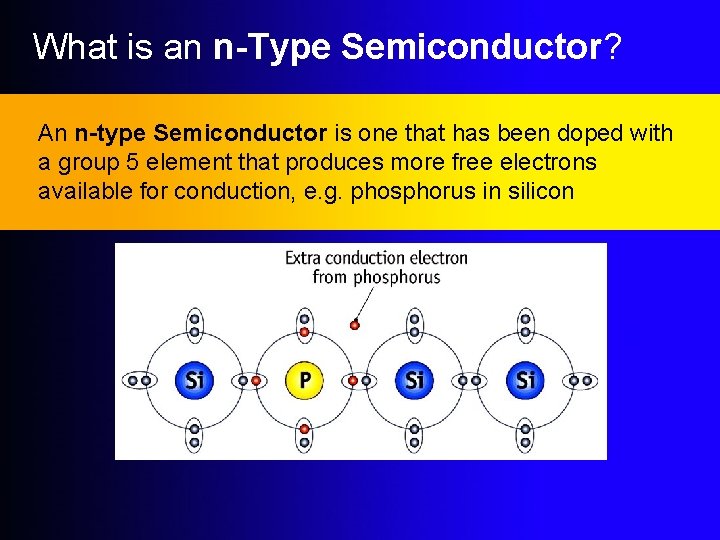
What is an n-Type Semiconductor? An n-type Semiconductor is one that has been doped with a group 5 element that produces more free electrons available for conduction, e. g. phosphorus in silicon

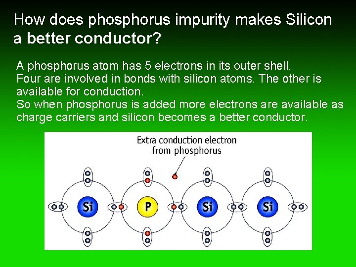
How does phosphorus impurity makes Silicon a better conductor? A phosphorus atom has 5 electrons in its outer shell. Four are involved in bonds with silicon atoms. The other is available for conduction. So when phosphorus is added more electrons are available as charge carriers and silicon becomes a better conductor.

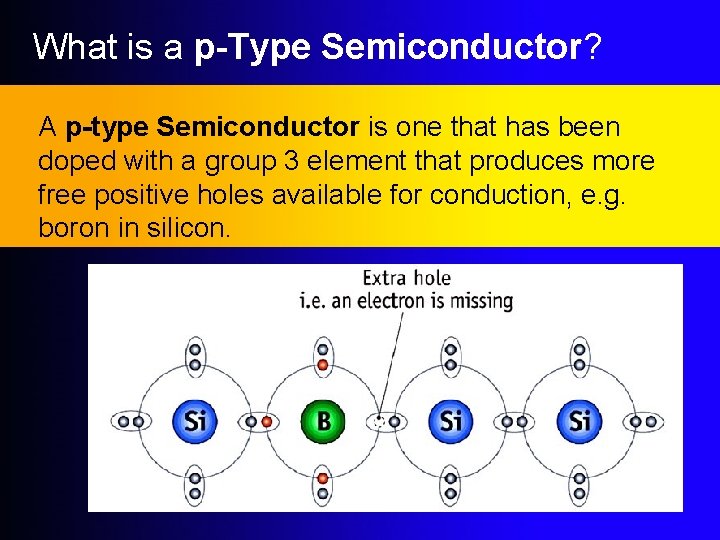
What is a p-Type Semiconductor? A p-type Semiconductor is one that has been doped with a group 3 element that produces more free positive holes available for conduction, e. g. boron in silicon.

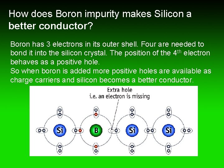
How does Boron impurity makes Silicon a better conductor? Boron has 3 electrons in its outer shell. Four are needed to bond it into the silicon crystal. The position of the 4 th electron behaves as a positive hole. So when boron is added more positive holes are available as charge carriers and silicon becomes a better conductor.

What is Extrinsic Conduction? Increased conduction in a semiconductor due to the addition of impurities is called Extrinsic Conduction. The semiconductor formed is called an Extrinsic Semiconductor.

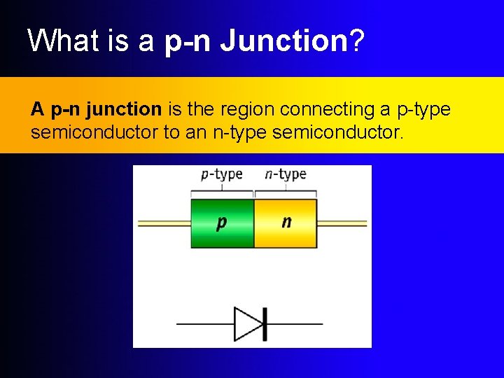
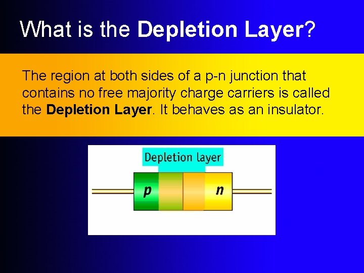
What is a p-n Junction? A p-n junction is the region connecting a p-type semiconductor to an n-type semiconductor.

What is the Depletion Layer? The region at both sides of a p-n junction that contains no free majority charge carriers is called the Depletion Layer. It behaves as an insulator.

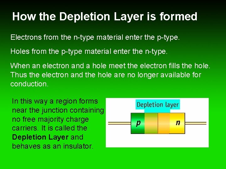
How the Depletion Layer is formed Electrons from the n-type material enter the p-type. Holes from the p-type material enter the n-type. When an electron and a hole meet the electron fills the hole. Thus the electron and the hole are no longer available for conduction. In this way a region forms near the junction containing no free majority charge carriers. It is called the Depletion Layer and behaves as an insulator.

Junction Voltage When electrons leave the n-type material and cross the junction, the ntype material becomes positively charged. Likewise holes entering it increase its positive charge. When enough positive charge accumulates in the n-type material no more electrons leave it - since they are attracted by the positive charge. In a similar way a negative charge accumulates in the p-type material as electrons enter it and holes leave it. The charge on both sides of the junction causes a small voltage to appear across the junction called the Junction Voltage. For Silicon at room temperature the Junction Voltage is somewhere between 0. 6 V and 0. 8 V.

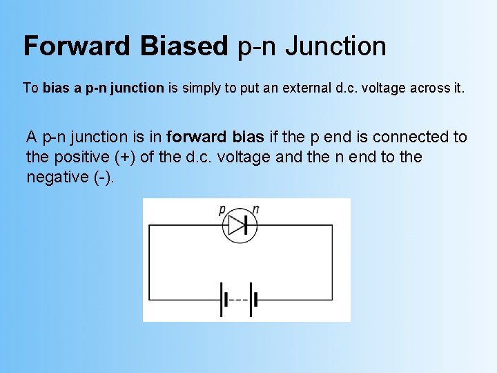
Forward Biased p-n Junction To bias a p-n junction is simply to put an external d. c. voltage across it. A p-n junction is in forward bias if the p end is connected to the positive (+) of the d. c. voltage and the n end to the negative (-).

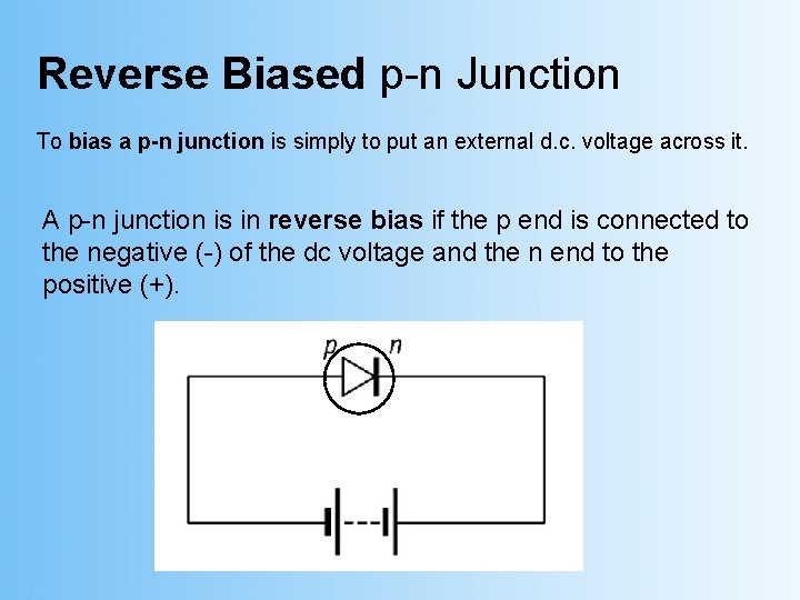
Reverse Biased p-n Junction To bias a p-n junction is simply to put an external d. c. voltage across it. A p-n junction is in reverse bias if the p end is connected to the negative (-) of the dc voltage and the n end to the positive (+).

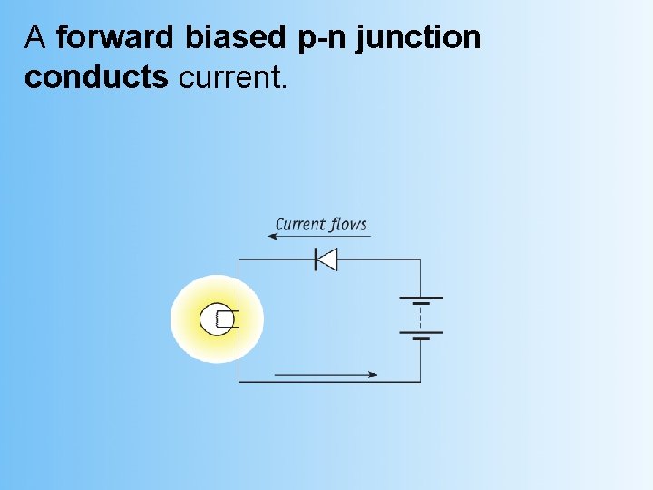
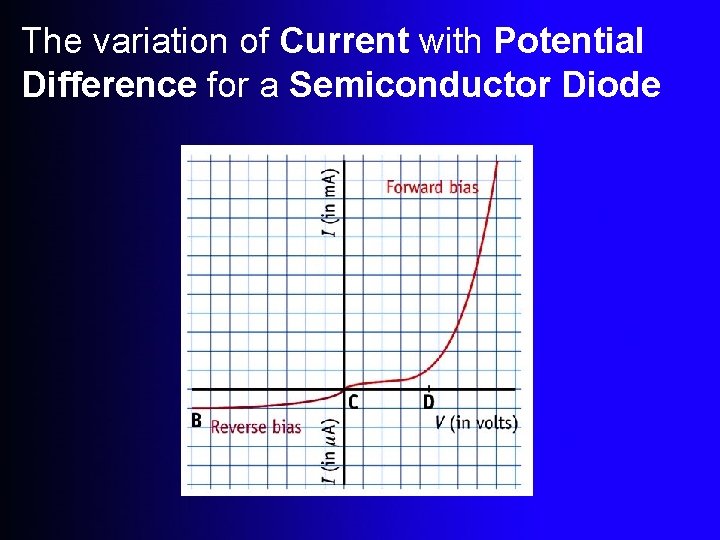
A forward biased p-n junction conducts current.

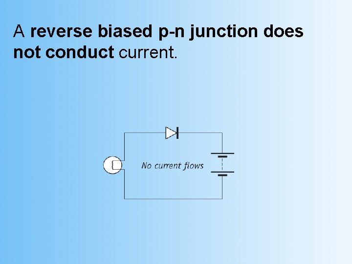
A reverse biased p-n junction does not conduct current.

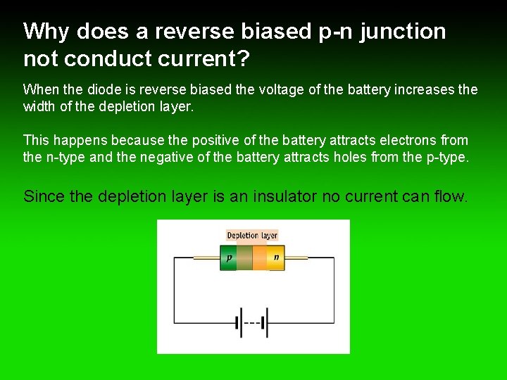
Why does a reverse biased p-n junction not conduct current? When the diode is reverse biased the voltage of the battery increases the width of the depletion layer. This happens because the positive of the battery attracts electrons from the n-type and the negative of the battery attracts holes from the p-type. Since the depletion layer is an insulator no current can flow.

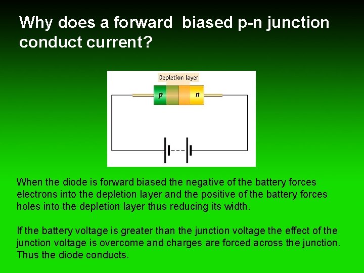
Why does a forward biased p-n junction conduct current? When the diode is forward biased the negative of the battery forces electrons into the depletion layer and the positive of the battery forces holes into the depletion layer thus reducing its width. If the battery voltage is greater than the junction voltage the effect of the junction voltage is overcome and charges are forced across the junction. Thus the diode conducts.

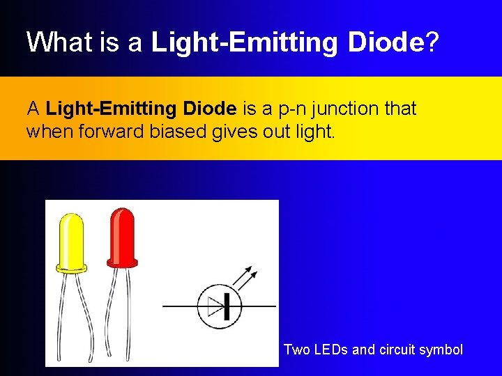
What is a Light-Emitting Diode? A Light-Emitting Diode is a p-n junction that when forward biased gives out light. Two LEDs and circuit symbol

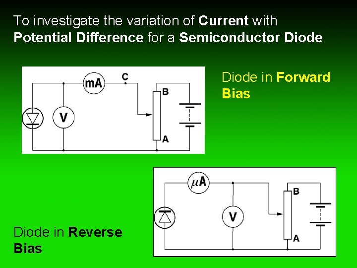
To investigate the variation of Current with Potential Difference for a Semiconductor Diode in Forward Bias Diode in Reverse Bias

The variation of Current with Potential Difference for a Semiconductor Diode

What is Rectification? Rectification is the Conversion of a. c. to d. c. A p-n diode can be used as a Rectifier.

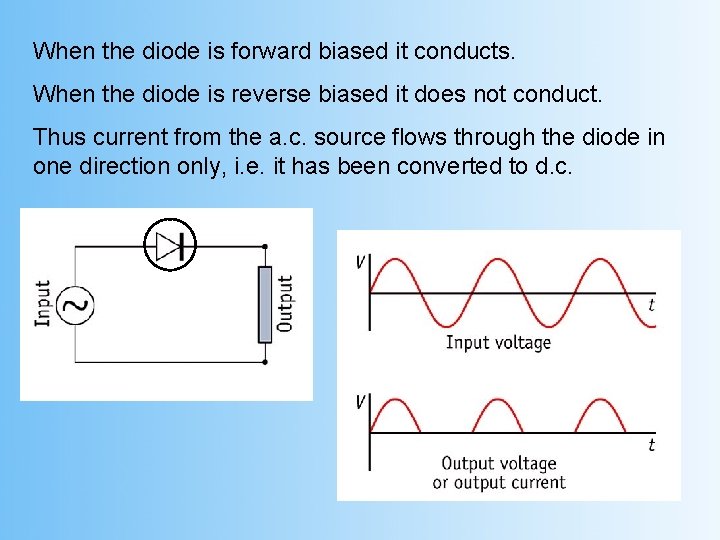
When the diode is forward biased it conducts. When the diode is reverse biased it does not conduct. Thus current from the a. c. source flows through the diode in one direction only, i. e. it has been converted to d. c.