Semiconductor spintronics in ferromagnetic and nonmagnetic pn junctions
![RHall [ ] SIHE detection at n 2 3 2 1 0 Vsd= 0 RHall [ ] SIHE detection at n 2 3 2 1 0 Vsd= 0](https://slidetodoc.com/presentation_image/9d5a2928bbb1470c4eb10ffde2befdab/image-32.jpg)

- Slides: 39

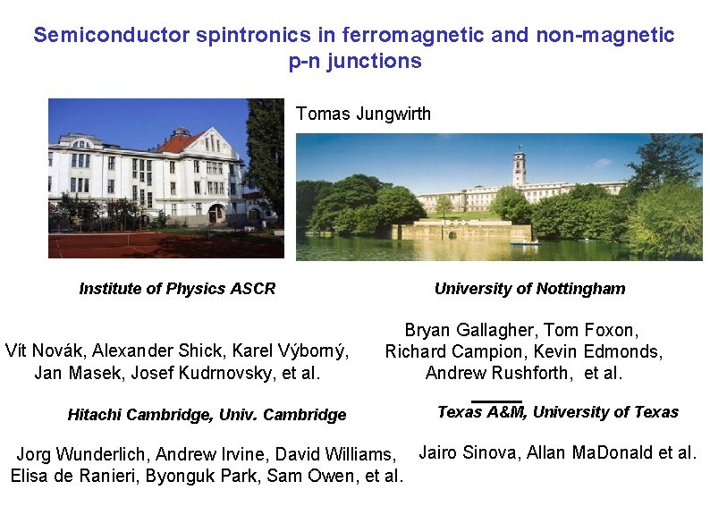
Semiconductor spintronics in ferromagnetic and non-magnetic p-n junctions Tomas Jungwirth Institute of Physics ASCR Vít Novák, Alexander Shick, Karel Výborný, Jan Masek, Josef Kudrnovsky, et al. Hitachi Cambridge, Univ. Cambridge University of Nottingham Bryan Gallagher, Tom Foxon, Richard Campion, Kevin Edmonds, Andrew Rushforth, et al. Texas A&M, University of Texas Jorg Wunderlich, Andrew Irvine, David Williams, Jairo Sinova, Allan Ma. Donald et al. Elisa de Ranieri, Byonguk Park, Sam Owen, et al.

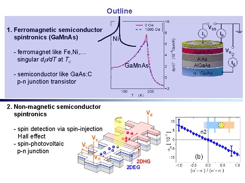
Outline 1. Ferromagnetic semiconductor spintronics (Ga. Mn. As) - ferromagnet like Fe, Ni, … singular d /d. T at Tc - semiconductor like Ga. As: C p-n junction transistor 2. Non-magnetic semiconductor spintronics - spin detection via spin-injection Hall effect - spin-photovoltaic p-n junction Ni Ga. Mn. As

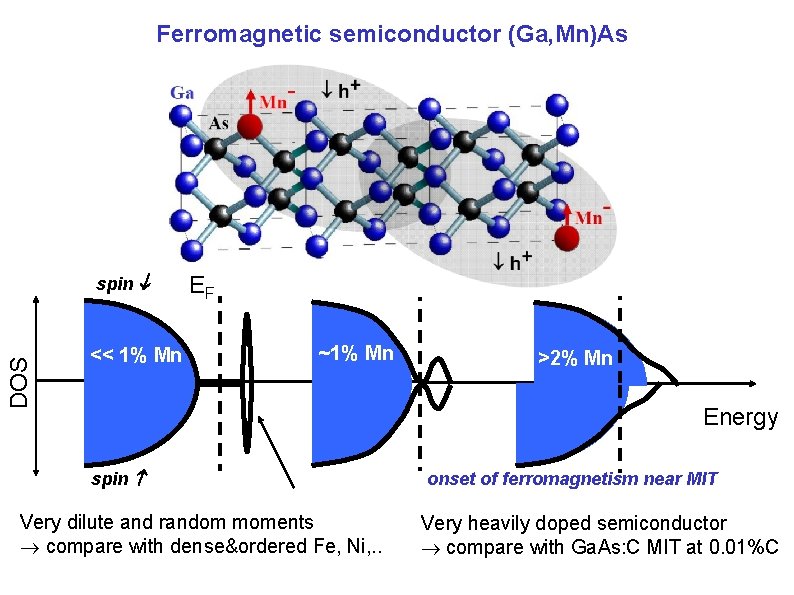
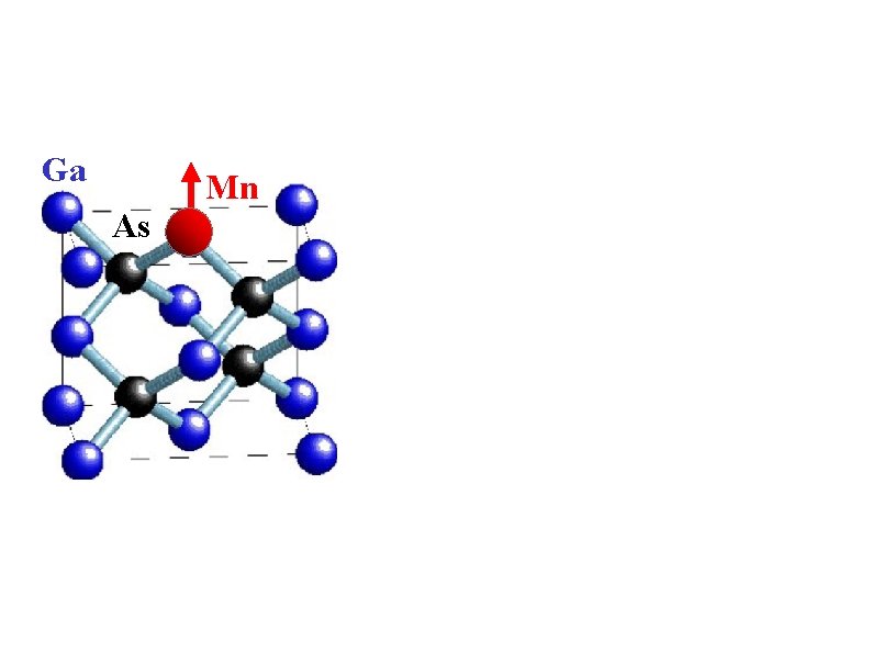
Ferromagnetic semiconductor (Ga, Mn)As DOS spin << 1% Mn EF ~1% Mn >2% Mn Energy spin Very dilute and random moments compare with dense&ordered Fe, Ni, . . onset of ferromagnetism near MIT Very heavily doped semiconductor compare with Ga. As: C MIT at 0. 01%C

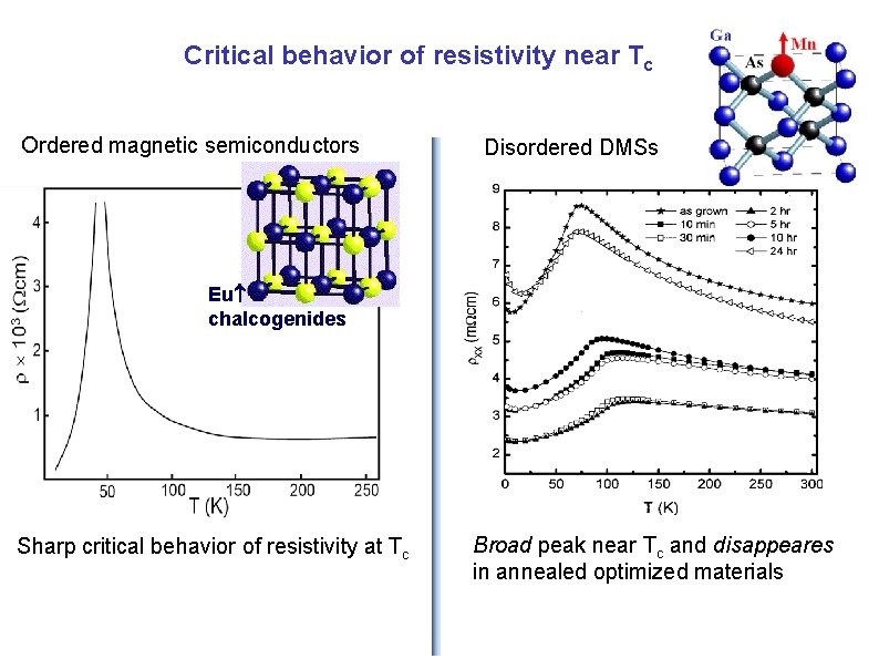
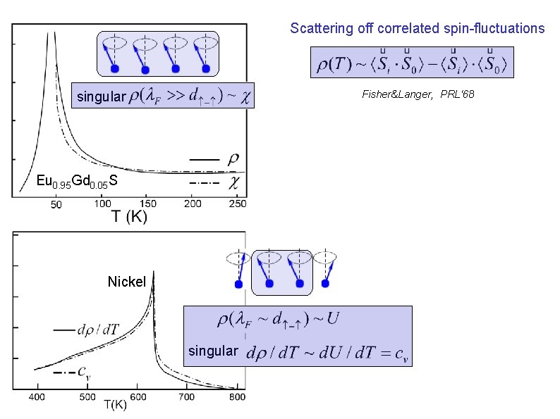
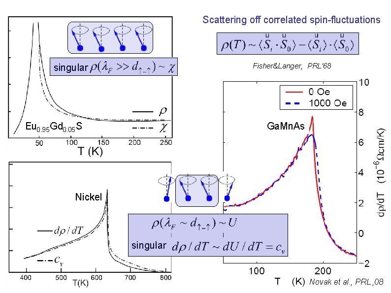
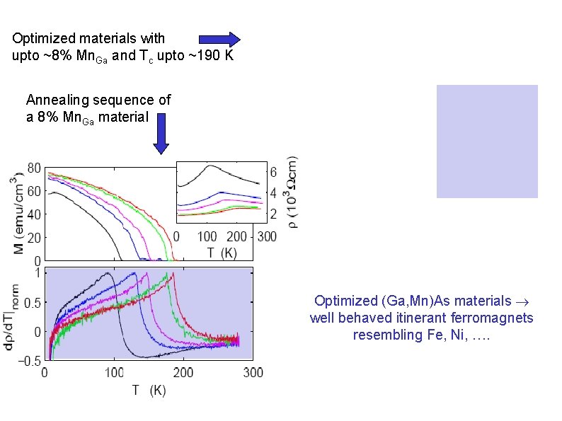
Critical behavior of resistivity near Tc Ordered magnetic semiconductors Disordered DMSs Eu chalcogenides Sharp critical behavior of resistivity at Tc Broad peak near Tc and disappeares in annealed optimized materials

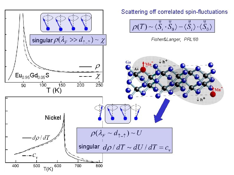
Scattering off correlated spin-fluctuations Fisher&Langer, PRL‘ 68 singular Eu 0. 95 Gd 0. 05 S Nickel singular

Scattering off correlated spin-fluctuations Fisher&Langer, PRL‘ 68 singular Eu 0. 95 Gd 0. 05 S Nickel singular

Scattering off correlated spin-fluctuations Fisher&Langer, PRL‘ 68 singular Eu 0. 95 Gd 0. 05 S Ga. Mn. As Nickel singular Novak et al. , PRL ‚ 08

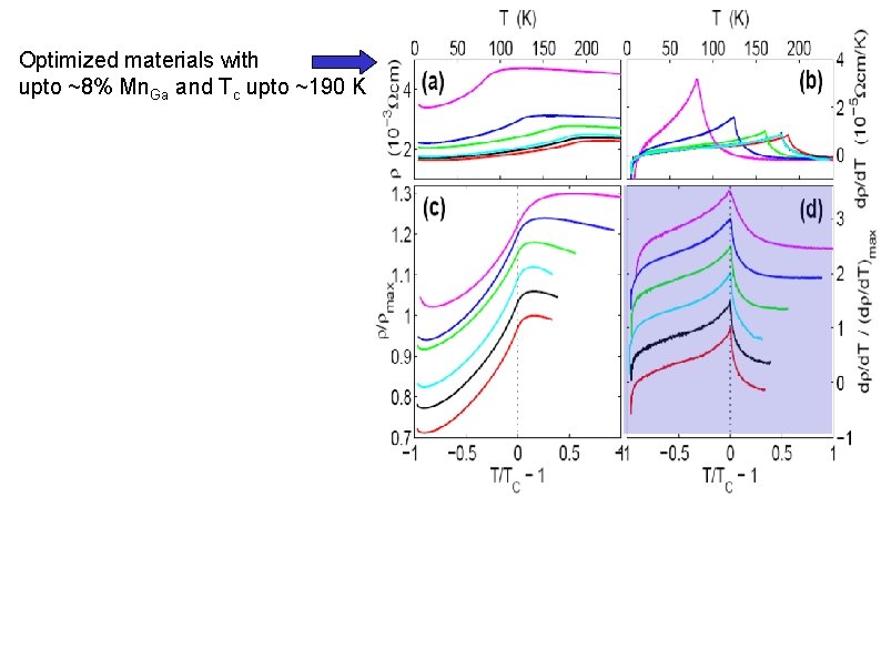
Optimized materials with upto ~8% Mn. Ga and Tc upto ~190 K

Optimized materials with upto ~8% Mn. Ga and Tc upto ~190 K Annealing sequence of a 8% Mn. Ga material Optimized (Ga, Mn)As materials well behaved itinerant ferromagnets resembling Fe, Ni, ….

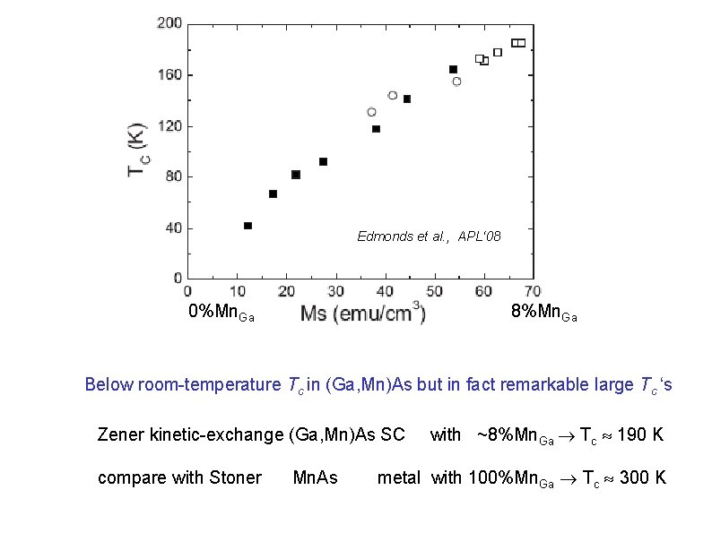
Edmonds et al. , APL‘ 08 0%Mn. Ga 8%Mn. Ga Below room-temperature Tc in (Ga, Mn)As but in fact remarkable large Tc ‘s Zener kinetic-exchange (Ga, Mn)As SC compare with Stoner Mn. As with ~8%Mn. Ga Tc 190 K metal with 100%Mn. Ga Tc 300 K

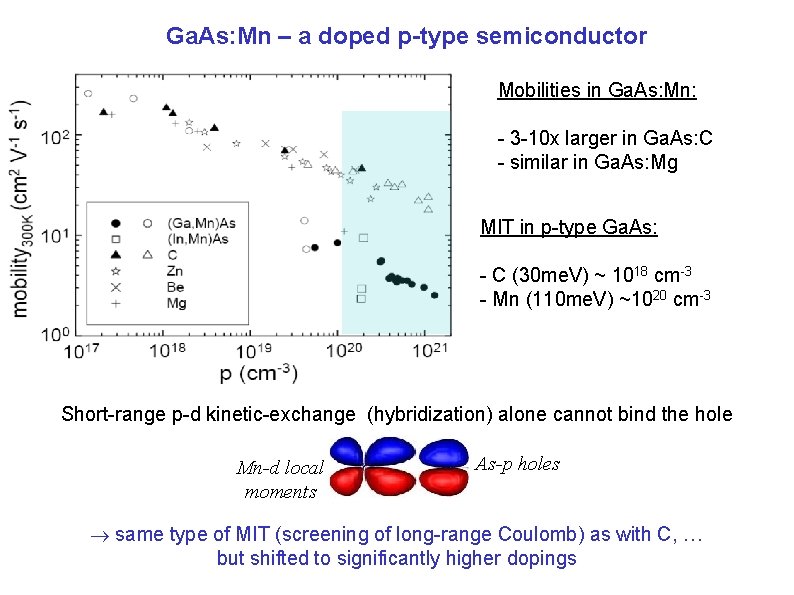
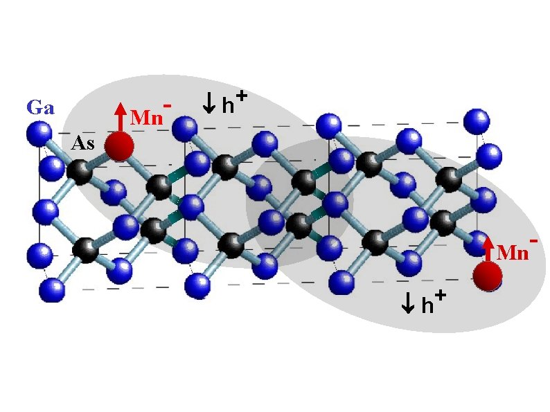
Ga. As: Mn – a doped p-type semiconductor Mobilities in Ga. As: Mn: - 3 -10 x larger in Ga. As: C - similar in Ga. As: Mg MIT in p-type Ga. As: - C (30 me. V) ~ 1018 cm-3 - Mn (110 me. V) ~1020 cm-3 Short-range p-d kinetic-exchange (hybridization) alone cannot bind the hole Mn-d local moments As-p holes same type of MIT (screening of long-range Coulomb) as with C, … but shifted to significantly higher dopings

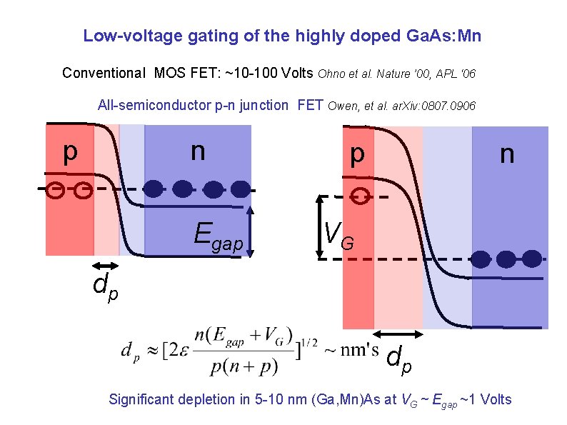
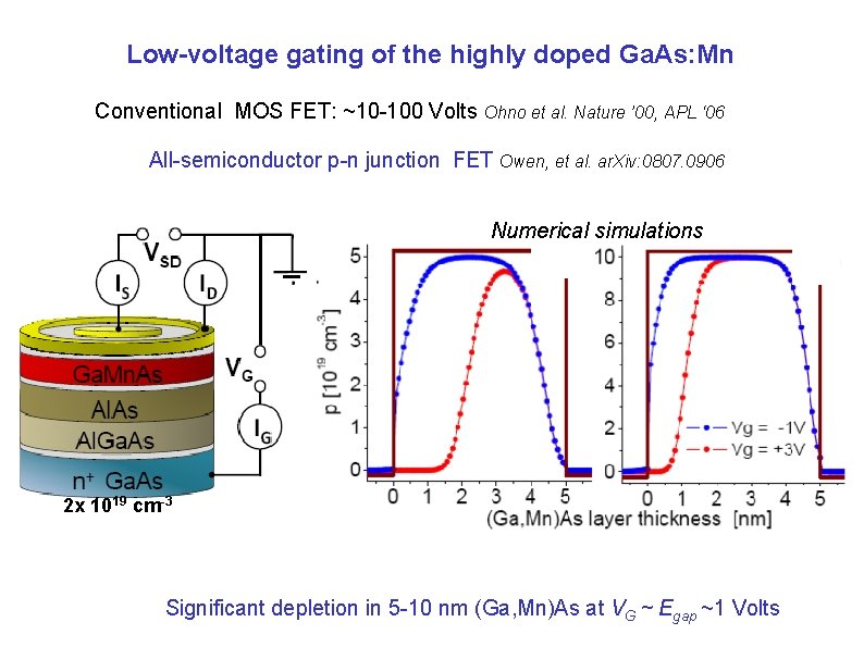
Low-voltage gating of the highly doped Ga. As: Mn Conventional MOS FET: ~10 -100 Volts Ohno et al. Nature ’ 00, APL ‘ 06 All-semiconductor p-n junction FET Owen, et al. ar. Xiv: 0807. 0906 p n Egap p n VG dp dp Significant depletion in 5 -10 nm (Ga, Mn)As at VG ~ Egap ~1 Volts

Low-voltage gating of the highly doped Ga. As: Mn Conventional MOS FET: ~10 -100 Volts Ohno et al. Nature ’ 00, APL ‘ 06 All-semiconductor p-n junction FET Owen, et al. ar. Xiv: 0807. 0906 Numerical simulations 2 x 1019 cm-3 Significant depletion in 5 -10 nm (Ga, Mn)As at VG ~ Egap ~1 Volts

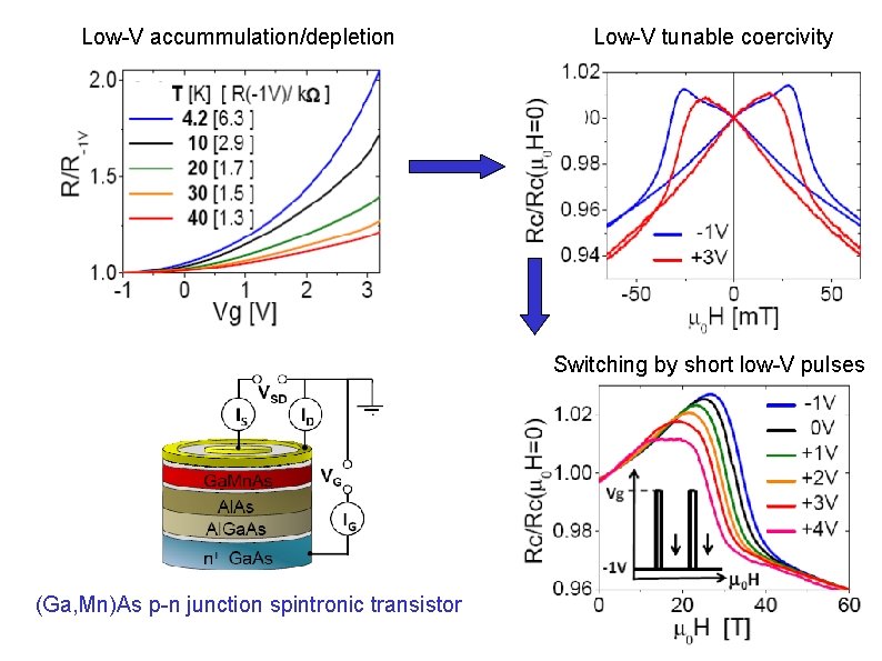
Low-V accummulation/depletion Low-V tunable coercivity Switching by short low-V pulses (Ga, Mn)As p-n junction spintronic transistor

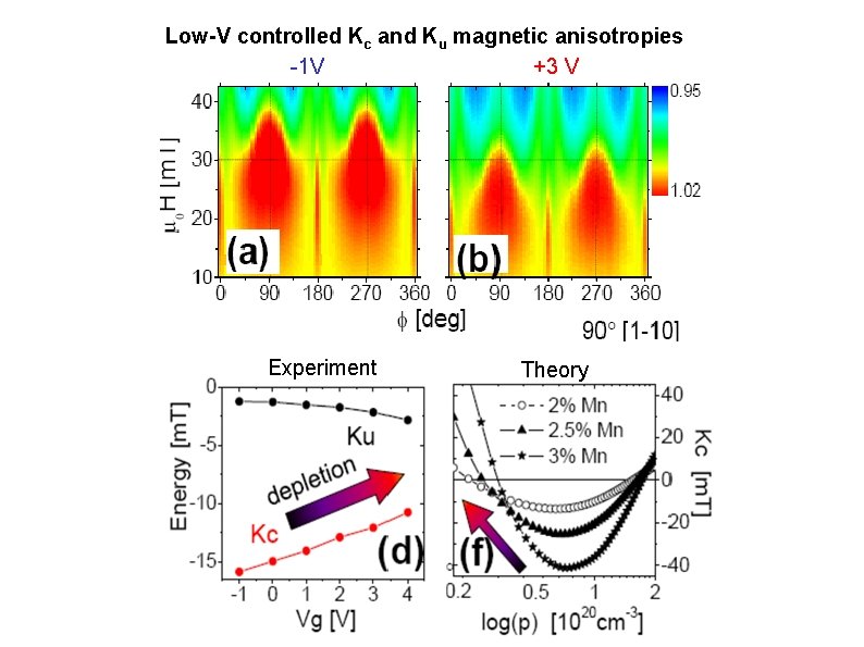
Low-V controlled Kc and Ku magnetic anisotropies -1 V +3 V Experiment Theory

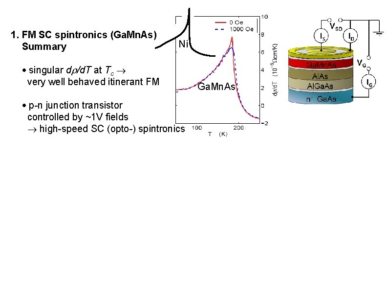
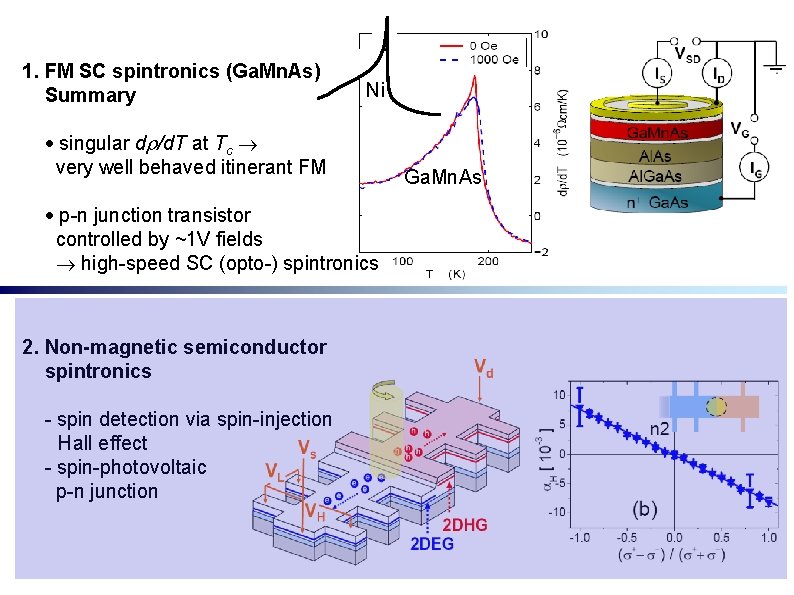
1. FM SC spintronics (Ga. Mn. As) Summary Ni singular d /d. T at Tc very well behaved itinerant FM p-n junction transistor controlled by ~1 V fields high-speed SC (opto-) spintronics Ga. Mn. As

1. FM SC spintronics (Ga. Mn. As) Summary Ni singular d /d. T at Tc very well behaved itinerant FM p-n junction transistor controlled by ~1 V fields high-speed SC (opto-) spintronics 2. Non-magnetic semiconductor spintronics - spin detection via spin-injection Hall effect - spin-photovoltaic p-n junction Ga. Mn. As

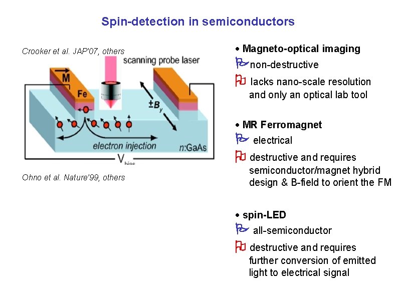
Spin-detection in semiconductors Crooker et al. JAP’ 07, others Magneto-optical imaging non-destructive lacks nano-scale resolution and only an optical lab tool MR Ferromagnet electrical destructive and requires Ohno et al. Nature’ 99, others semiconductor/magnet hybrid design & B-field to orient the FM spin-LED all-semiconductor destructive and requires further conversion of emitted light to electrical signal

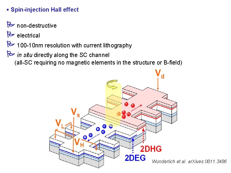
Spin-injection Hall effect non-destructive electrical 100 -10 nm resolution with current lithography in situ directly along the SC channel (all-SC requiring no magnetic elements in the structure or B-field) Wunderlich et al. ar. Xives: 0811. 3486

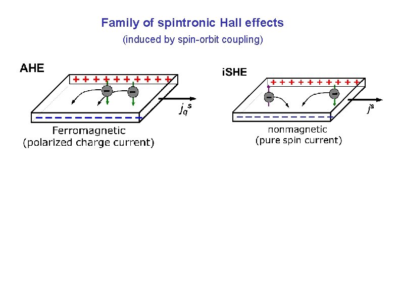
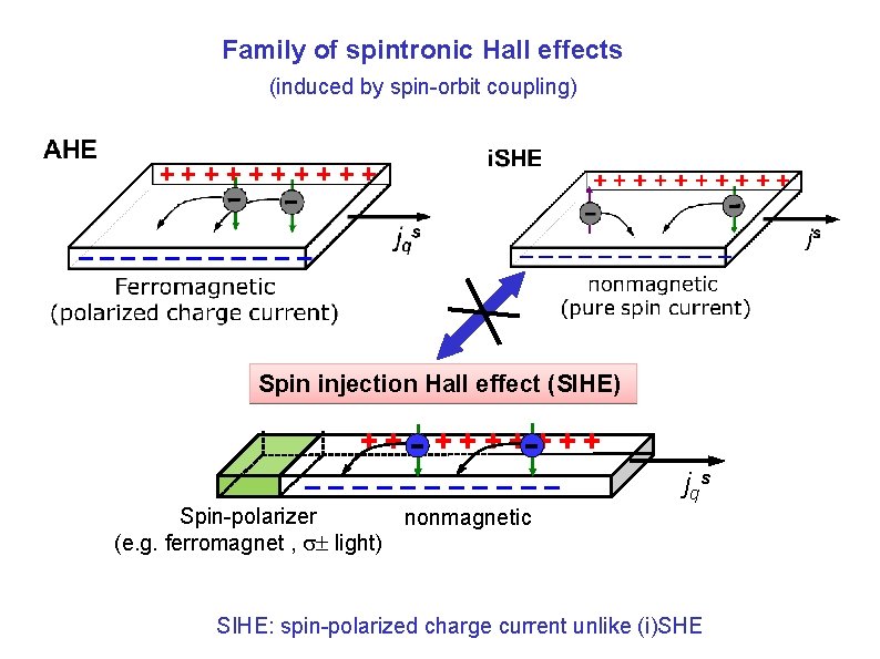
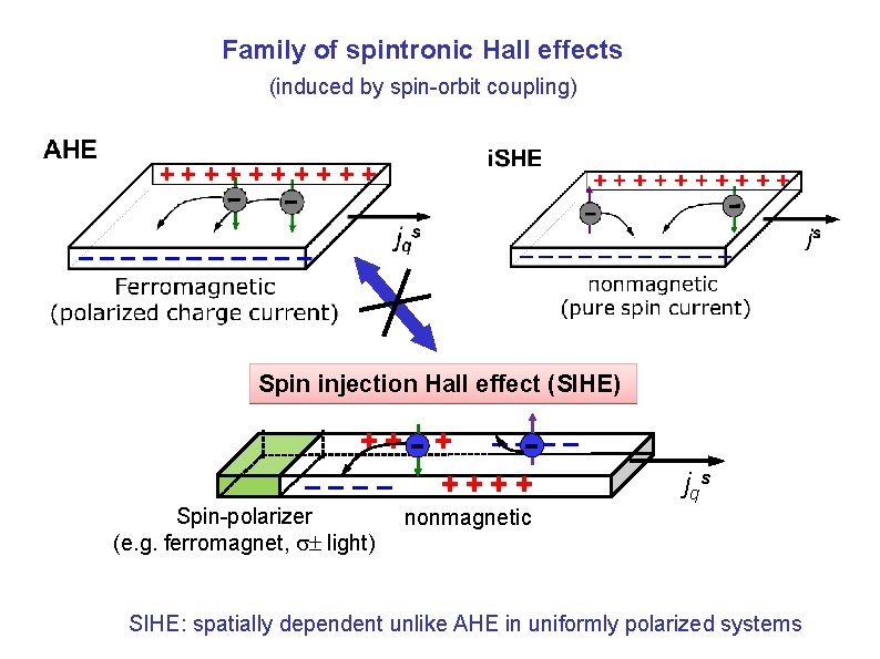
Family of spintronic Hall effects (induced by spin-orbit coupling)

Family of spintronic Hall effects (induced by spin-orbit coupling) Spin injection Hall effect (SIHE) +++++ –––––– Spin-polarizer (e. g. ferromagnet , light) j qs nonmagnetic SIHE: spin-polarized charge current unlike (i)SHE

Family of spintronic Hall effects (induced by spin-orbit coupling) Spin injection Hall effect (SIHE) ++++ –––– ++++ Spin-polarizer (e. g. ferromagnet, light) j qs nonmagnetic SIHE: spatially dependent unlike AHE in uniformly polarized systems

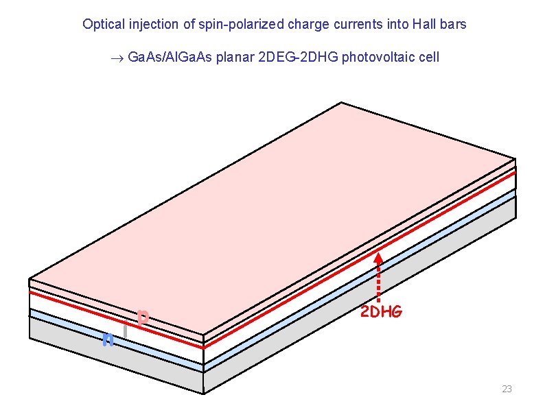
Optical injection of spin-polarized charge currents into Hall bars Ga. As/Al. Ga. As planar 2 DEG-2 DHG photovoltaic cell ni p 2 DHG 23

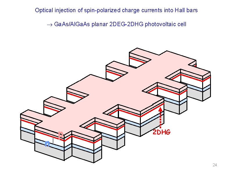
Optical injection of spin-polarized charge currents into Hall bars Ga. As/Al. Ga. As planar 2 DEG-2 DHG photovoltaic cell - ni p 2 DHG 24

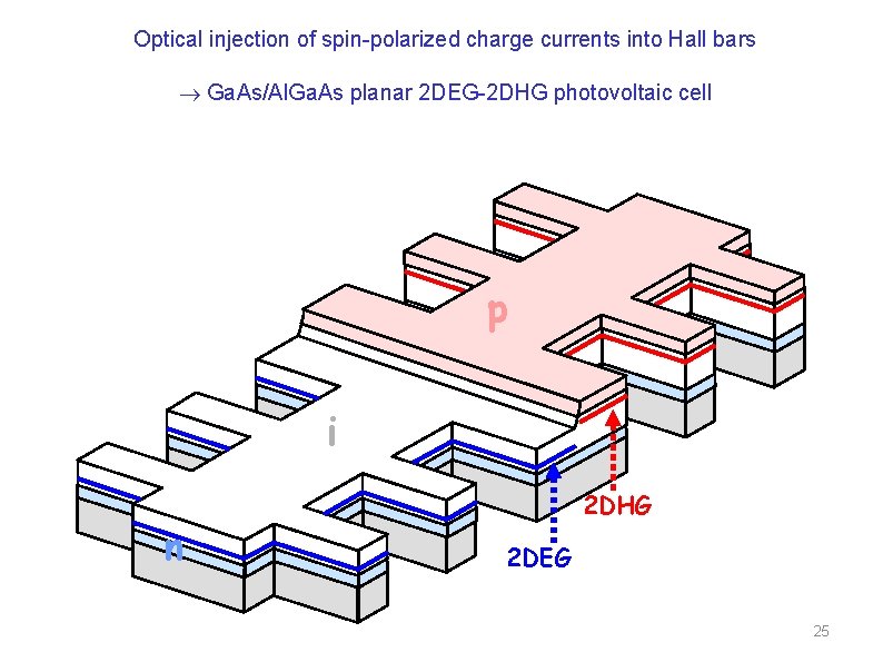
Optical injection of spin-polarized charge currents into Hall bars Ga. As/Al. Ga. As planar 2 DEG-2 DHG photovoltaic cell p i n 2 DHG 2 DEG 25

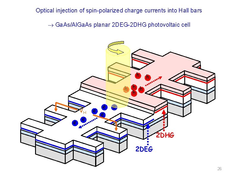
Optical injection of spin-polarized charge currents into Hall bars Ga. As/Al. Ga. As planar 2 DEG-2 DHG photovoltaic cell h h h e VH e e e 2 DHG 2 DEG 26

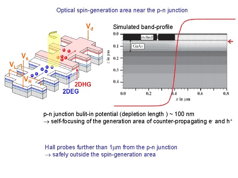
Optical spin-generation area near the p-n junction Simulated band-profile p-n junction bulit-in potential (depletion length ) ~ 100 nm self-focusing of the generation area of counter-propagating e- and h+ Hall probes further than 1 m from the p-n junction safely outside the spin-generation area

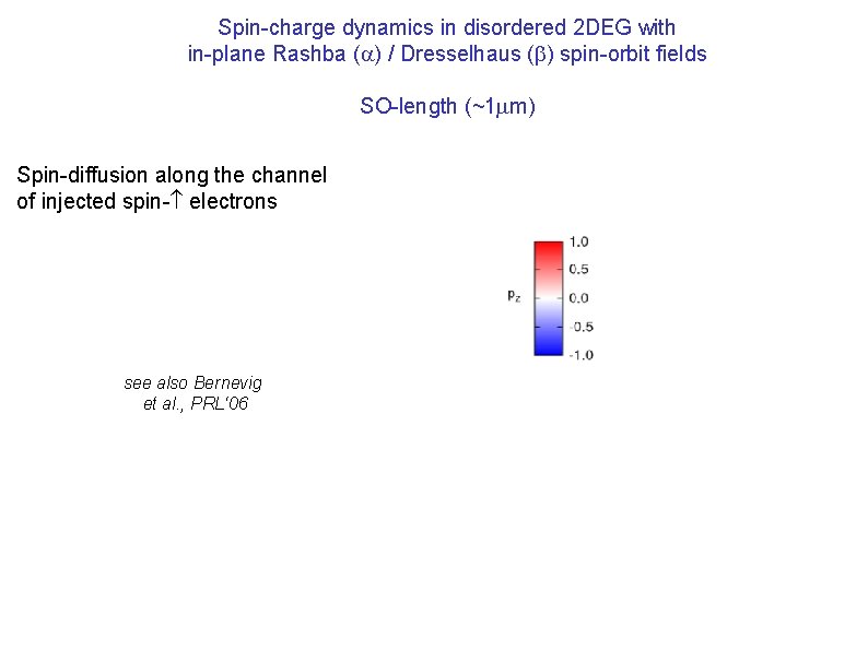
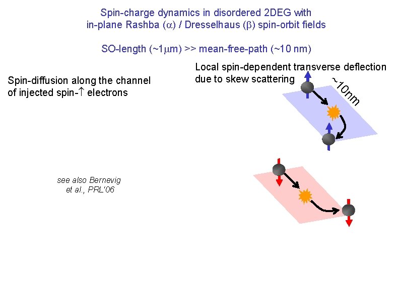
Spin-charge dynamics in disordered 2 DEG with in-plane Rashba ( ) / Dresselhaus ( ) spin-orbit fields SO-length (~1 m) Spin-diffusion along the channel of injected spin- electrons see also Bernevig et al. , PRL‘ 06

Spin-charge dynamics in disordered 2 DEG with in-plane Rashba ( ) / Dresselhaus ( ) spin-orbit fields SO-length (~1 m) >> mean-free-path (~10 nm) m 0 n ~1 Spin-diffusion along the channel of injected spin- electrons Local spin-dependent transverse deflection due to skew scattering see also Bernevig et al. , PRL‘ 06

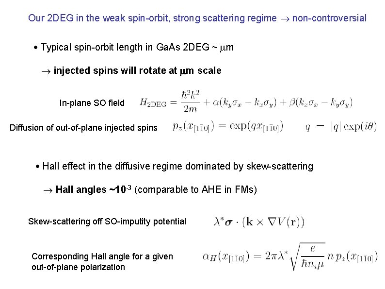
Our 2 DEG in the weak spin-orbit, strong scattering regime non-controversial Typical spin-orbit length in Ga. As 2 DEG ~ m injected spins will rotate at m scale In-plane SO field Diffusion of out-of-plane injected spins Hall effect in the diffusive regime dominated by skew-scattering Hall angles ~10 -3 (comparable to AHE in FMs) Skew-scattering off SO-imputity potential Corresponding Hall angle for a given out-of-plane polarization

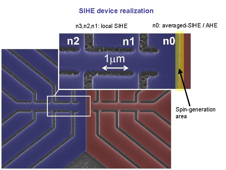
SIHE device realization n 3, n 2, n 1: local SIHE 3 2 1 0 n 0: averaged-SIHE / AHE Spin-generation area
![RHall SIHE detection at n 2 3 2 1 0 Vsd 0 RHall [ ] SIHE detection at n 2 3 2 1 0 Vsd= 0](https://slidetodoc.com/presentation_image/9d5a2928bbb1470c4eb10ffde2befdab/image-32.jpg)
RHall [ ] SIHE detection at n 2 3 2 1 0 Vsd= 0 V +

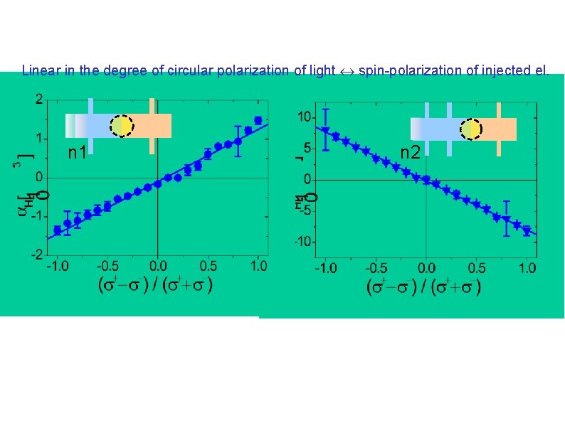
Linear in the degree of circular polarization of light spin-polarization of injected el. n 1 n 2

SIHE survives to high temperatures - +

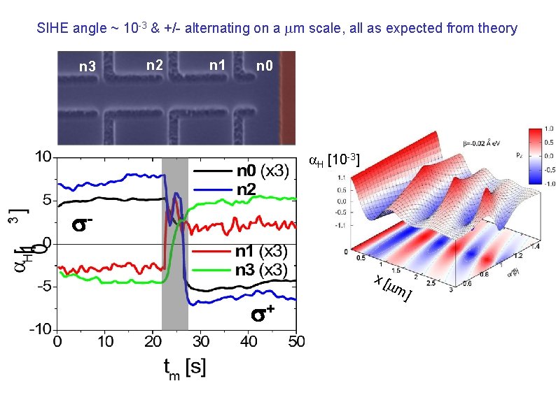
SIHE angle ~ 10 -3 & +/- alternating on a m scale, all as expected from theory n 3 n 2 n 1 n 0 H [10 -3] x[ + m ]

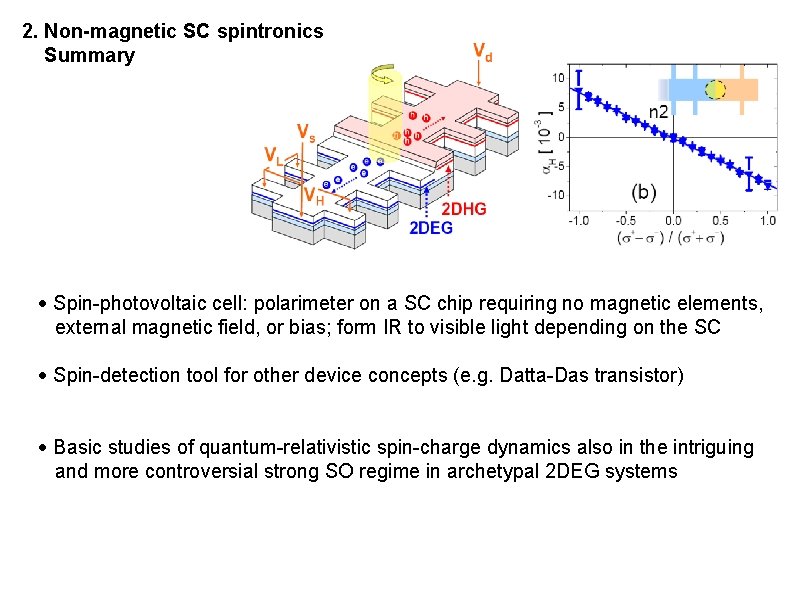
2. Non-magnetic SC spintronics Summary Spin-photovoltaic cell: polarimeter on a SC chip requiring no magnetic elements, external magnetic field, or bias; form IR to visible light depending on the SC Spin-detection tool for other device concepts (e. g. Datta-Das transistor) Basic studies of quantum-relativistic spin-charge dynamics also in the intriguing and more controversial strong SO regime in archetypal 2 DEG systems


Mn Ga h+ As Mn + h

Ga Mn As