SEMICONDUCTOR PHYSICS NEW AGE LIGHTING TECHNOLOGIES THEN AND

![REFERENCES [1]D. Neamon, Semiconductor Physics and Devices, 4 th ed. New York, NY: Mc. REFERENCES [1]D. Neamon, Semiconductor Physics and Devices, 4 th ed. New York, NY: Mc.](https://slidetodoc.com/presentation_image_h2/ab11ab741dd313af87a88fc61992191b/image-18.jpg)
- Slides: 18

SEMICONDUCTOR PHYSICS NEW AGE LIGHTING TECHNOLOGIES THEN AND NOW HUCK GREEN GRADUATE STUDENT UNIVERSITY OF NEW MEXICO SCHOOL OF ELECTRICAL ENGINEERING

LED TECHNOLOGIES • Brief LED History • Advantages to LEDs • Typical Led Structure • Current Vs. Voltage Characteristics • Semiconductor Material Properties for Photon Emission • Carrier Recombination • LED Efficiency • Future Technologies

BRIEF LED HISTORY • Electro luminesce phenomena first discovered by Henry J Round of Marconi labs in 1907. • Soviet inventor Oleg Losev conceived idea of first LED in 1927. • In 1951 LED physics was explained. Thanks to semiconductor physics and the transistor • 1961, Texas Instruments, Ga. As emitted infrared light. Process used a zinc diffused p-n junction with a spaced cathode contact to allow light to pass. Considered the first practical LED. • 1962, first visible LED (red) developed by nick Holonyak at General Electric. Ge material • Until 1968 LEDs were on the order of $200 per unit. • Monsanto company was the first to mass produce red LEDs using Ga. As. P. • In 1972, M. George Craford, a grad student of Holonyak invented the first yellow LED and improved brightness of red LEDs by a factor of 10. LED price dramatically reduced ~ $0. 05 unit. • 1993 Shuji Nakamura develops first bright blue LED using In. Ga. N (Nichia corporation). • Isamu Akasaki and Hiroshi Amano worked on developing the Ga. N nucleation on sapphire

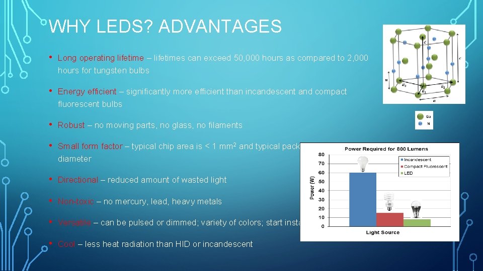
WHY LEDS? ADVANTAGES • Long operating lifetime – lifetimes can exceed 50, 000 hours as compared to 2, 000 hours for tungsten bulbs • Energy efficient – significantly more efficient than incandescent and compact fluorescent bulbs • Robust – no moving parts, no glass, no filaments • Small form factor – typical chip area is < 1 mm 2 and typical package is < 5 mm in diameter • Directional – reduced amount of wasted light • Non-toxic – no mercury, lead, heavy metals • Versatile – can be pulsed or dimmed; variety of colors; start instantly • Cool – less heat radiation than HID or incandescent

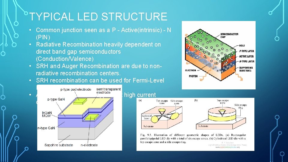
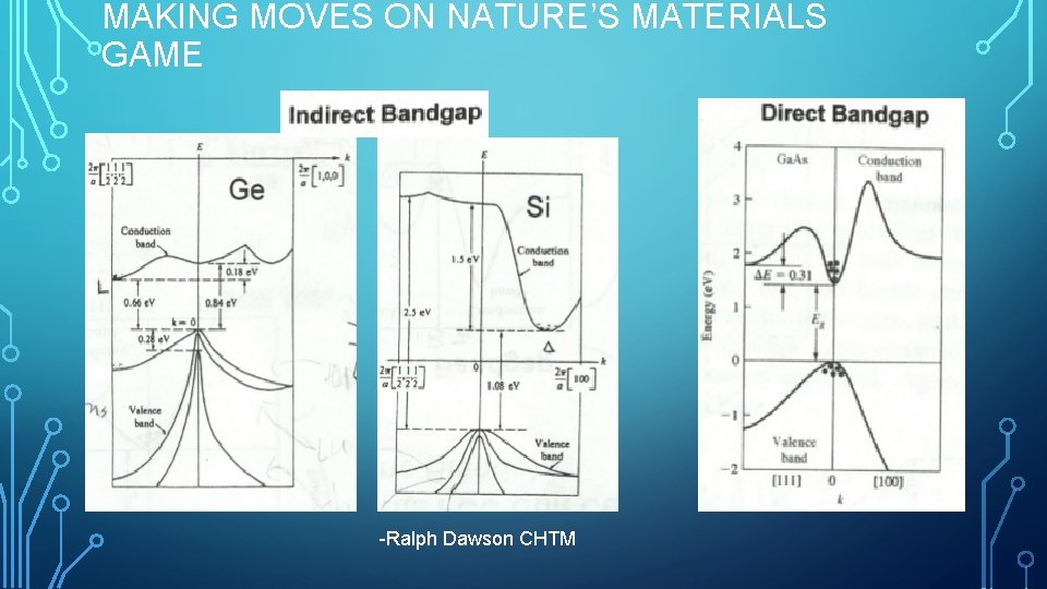
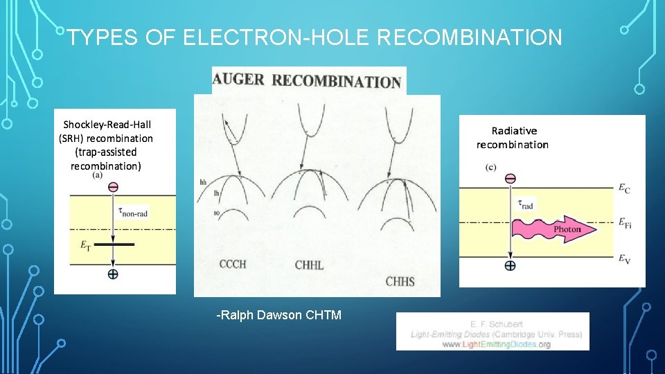
TYPICAL LED STRUCTURE • Common junction seen as a P - Active(intrinsic) - N (PIN) • Radiative Recombination heavily dependent on direct band gap semiconductors (Conduction/Valence) • SRH and Auger Recombination are due to nonradiative recombination centers. • SRH recombination can be used for Fermi-Level Pinning • Auger recombination happens at high current densities

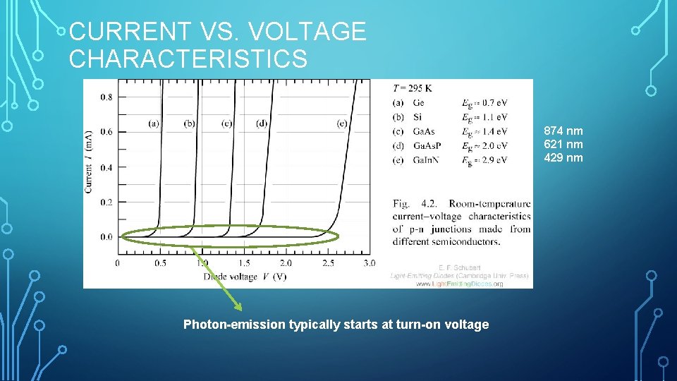
CURRENT VS. VOLTAGE CHARACTERISTICS 874 nm 621 nm 429 nm Photon-emission typically starts at turn-on voltage

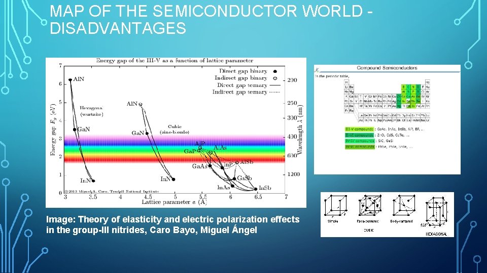
MAP OF THE SEMICONDUCTOR WORLD DISADVANTAGES Image: Theory of elasticity and electric polarization effects in the group-III nitrides, Caro Bayo, Miguel Ángel

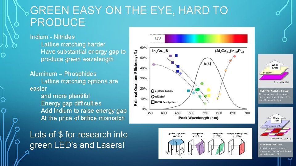
GREEN EASY ON THE EYE, HARD TO PRODUCE Indium - Nitrides Lattice matching harder Have substantial energy gap to produce green wavelength Aluminum – Phosphides Lattice matching options are easier and more plentiful Energy gap difficulties Add Indium to raise energy gap At the price of lattice mismatch Lots of $ for research into green LED’s and Lasers!

MAKING MOVES ON NATURE’S MATERIALS GAME -Ralph Dawson CHTM

TYPES OF ELECTRON-HOLE RECOMBINATION -Ralph Dawson CHTM

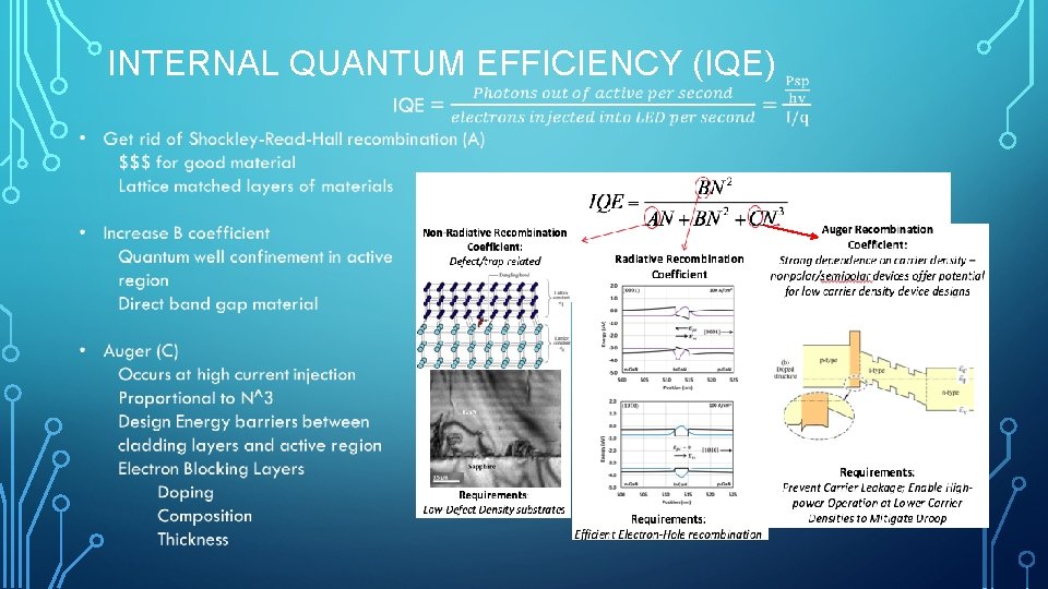
INTERNAL QUANTUM EFFICIENCY (IQE)

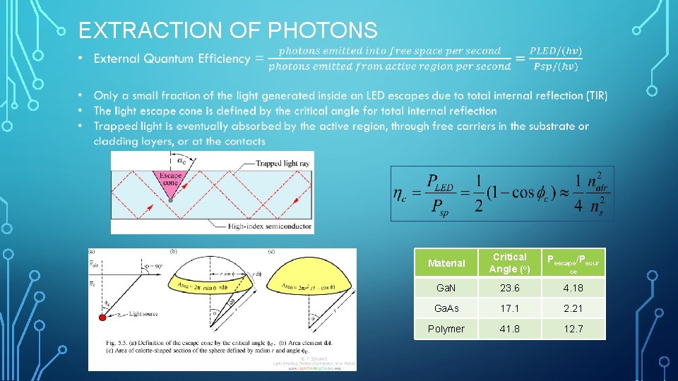
EXTRACTION OF PHOTONS Material Critical Angle (o) Pescape/Psour Ga. N 23. 6 4. 18 Ga. As 17. 1 2. 21 Polymer 41. 8 12. 7 ce

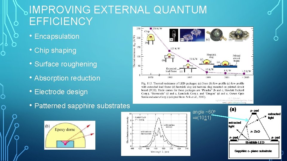
IMPROVING EXTERNAL QUANTUM EFFICIENCY • Encapsulation • Chip shaping • Surface roughening • Absorption reduction • Electrode design • Patterned sapphire substrates angle ~60 o (1011)

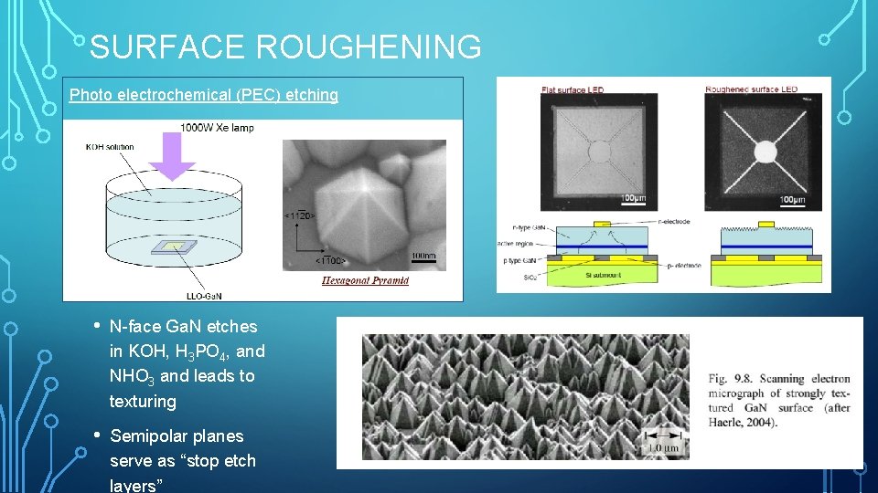
SURFACE ROUGHENING Photo electrochemical (PEC) etching • N-face Ga. N etches in KOH, H 3 PO 4, and NHO 3 and leads to texturing • Semipolar planes serve as “stop etch layers”

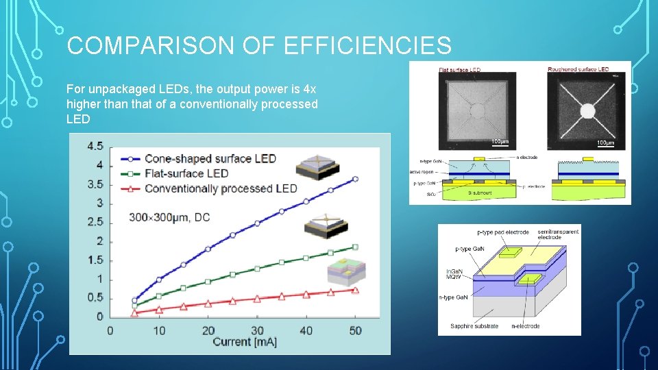
COMPARISON OF EFFICIENCIES For unpackaged LEDs, the output power is 4 x higher than that of a conventionally processed LED

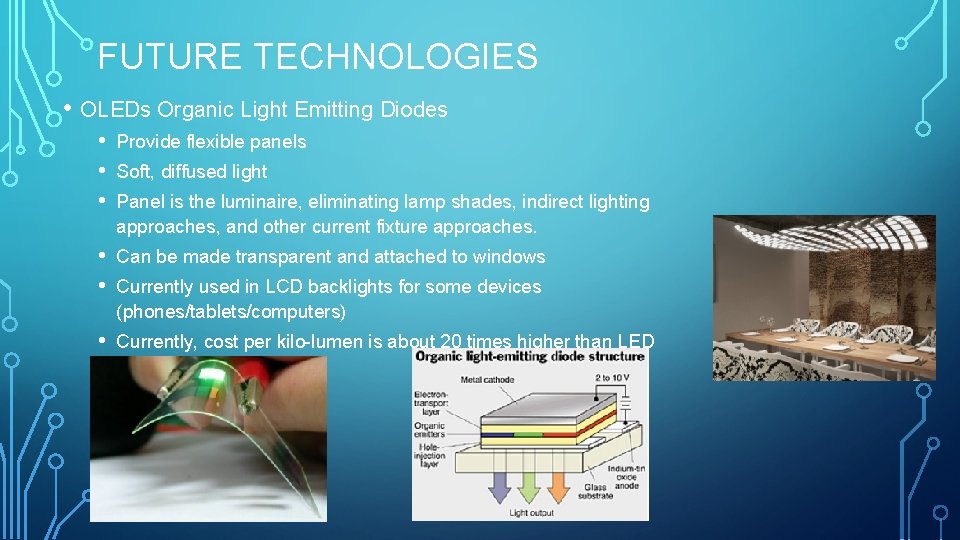
FUTURE TECHNOLOGIES • OLEDs Organic Light Emitting Diodes • • • Provide flexible panels • • Can be made transparent and attached to windows • Currently, cost per kilo-lumen is about 20 times higher than LED ~$200/klm Soft, diffused light Panel is the luminaire, eliminating lamp shades, indirect lighting approaches, and other current fixture approaches. Currently used in LCD backlights for some devices (phones/tablets/computers)

QUESTIONS?
![REFERENCES 1D Neamon Semiconductor Physics and Devices 4 th ed New York NY Mc REFERENCES [1]D. Neamon, Semiconductor Physics and Devices, 4 th ed. New York, NY: Mc.](https://slidetodoc.com/presentation_image_h2/ab11ab741dd313af87a88fc61992191b/image-18.jpg)
REFERENCES [1]D. Neamon, Semiconductor Physics and Devices, 4 th ed. New York, NY: Mc. Graw-Hill, 2012. [2]L. Coldren, S. Corzine and M. Mashanovitch, Diode lasers and photonic integrated circuits. Hoboken, N. J. : Wiley, 2012. [3]"lightemittingdiodes. org", Lightemittingdiodes. org, 2016. [Online]. Available: http: //www. lightemittingdiodes. org. [Accessed: 27 - Apr- 2016]. [4]R. Dawson, "Conduction Band Theory", UNM -CHTM, 2016.