Semiconductor Memories Lecture 1 May 10 2006 EE

![MOS NAND ROM V DD Pull-up devices BL [0] BL [1] BL [2] BL MOS NAND ROM V DD Pull-up devices BL [0] BL [1] BL [2] BL](https://slidetodoc.com/presentation_image/46fc78929f0db8279226b3477e7bae27/image-13.jpg)
- Slides: 24

Semiconductor Memories Lecture 1: May 10, 2006 EE Summer Camp Abhinav Agarwal

Outline n n n Concept/need of memory Parameters Types/classification Basic features Basic Cell circuits Peripheral circuitry

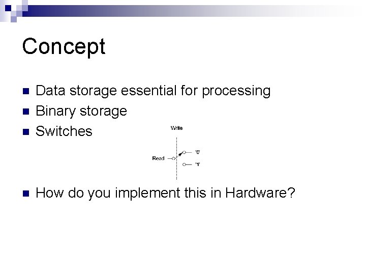
Concept n Data storage essential for processing Binary storage Switches n How do you implement this in Hardware? n n

Requirements n n Easy reading Easy Writing High density Speed, more speed and still more speed

Memory Chip Configuration

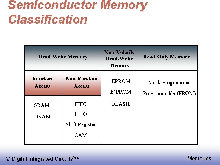
Semiconductor Memory Classification Read-Write Memory Random Access Non-Random Access SRAM FIFO DRAM LIFO Non-Volatile Read-Write Memory Read-Only Memory EPROM Mask-Programmed E 2 PROM Programmable (PROM) FLASH Shift Register CAM © Digital Integrated Circuits 2 nd Memories

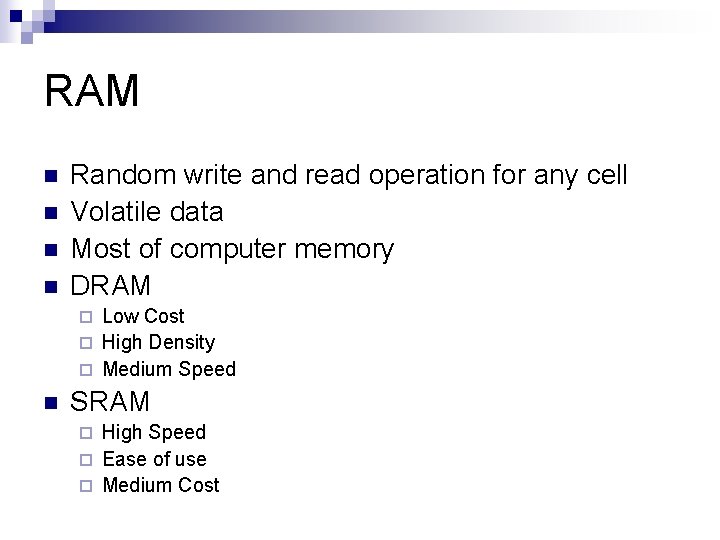
RAM n n Random write and read operation for any cell Volatile data Most of computer memory DRAM Low Cost ¨ High Density ¨ Medium Speed ¨ n SRAM High Speed ¨ Ease of use ¨ Medium Cost ¨

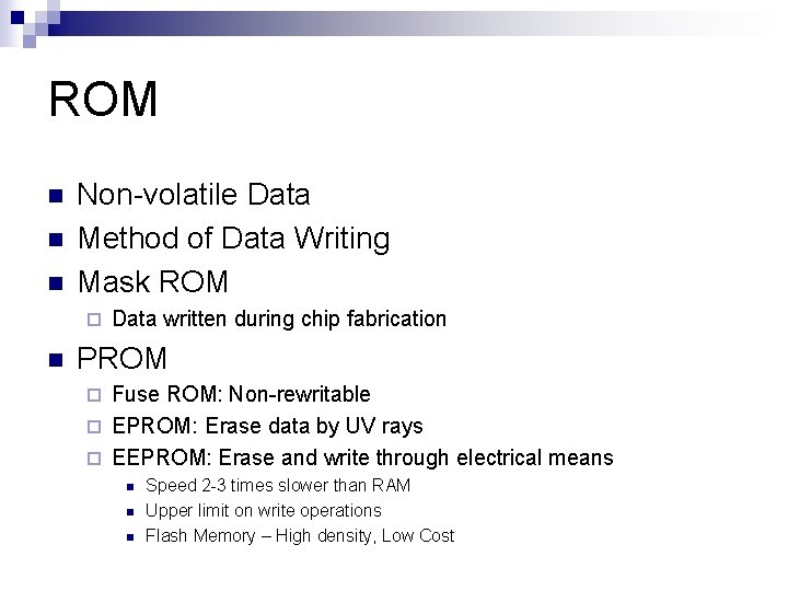
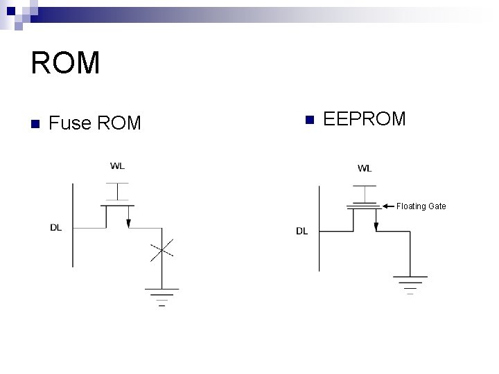
ROM n n n Non-volatile Data Method of Data Writing Mask ROM ¨ n Data written during chip fabrication PROM Fuse ROM: Non-rewritable ¨ EPROM: Erase data by UV rays ¨ EEPROM: Erase and write through electrical means ¨ n n n Speed 2 -3 times slower than RAM Upper limit on write operations Flash Memory – High density, Low Cost

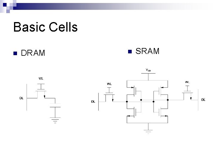
Basic Cells n DRAM n SRAM

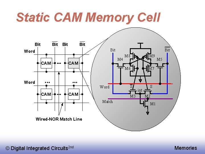
Static CAM Memory Cell Bit Bit Bit Word CAM Word • • • CAM • • • M 4 CAM • • • Bit Word CAM M 8 M 9 M 6 M 7 S M 3 Match int M 5 S M 2 M 1 Wired-NOR Match Line © Digital Integrated Circuits 2 nd Memories

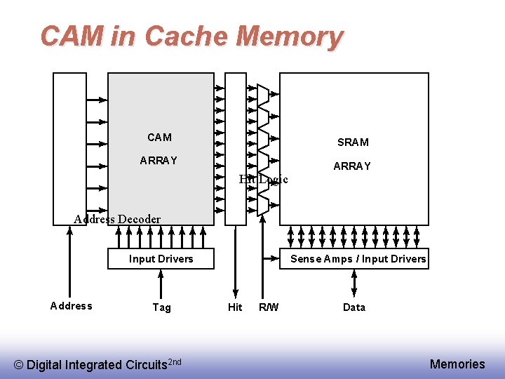
CAM in Cache Memory CAM SRAM ARRAY Hit Logic Address Decoder Input Drivers Address Tag © Digital Integrated Circuits 2 nd Sense Amps / Input Drivers Hit R/W Data Memories

ROM n Fuse ROM n EEPROM Floating Gate
![MOS NAND ROM V DD Pullup devices BL 0 BL 1 BL 2 BL MOS NAND ROM V DD Pull-up devices BL [0] BL [1] BL [2] BL](https://slidetodoc.com/presentation_image/46fc78929f0db8279226b3477e7bae27/image-13.jpg)
MOS NAND ROM V DD Pull-up devices BL [0] BL [1] BL [2] BL [3] WL [0] WL [1] WL [2] WL [3] All word lines high by default with exception of selected row © Digital Integrated Circuits 2 nd Memories

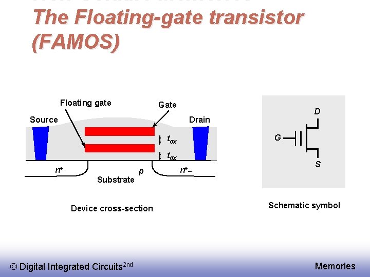
Non-Volatile Memories The Floating-gate transistor (FAMOS) Floating gate Gate Source D Drain G tox n+ Substrate p Device cross-section © Digital Integrated Circuits 2 nd n+_ S Schematic symbol Memories

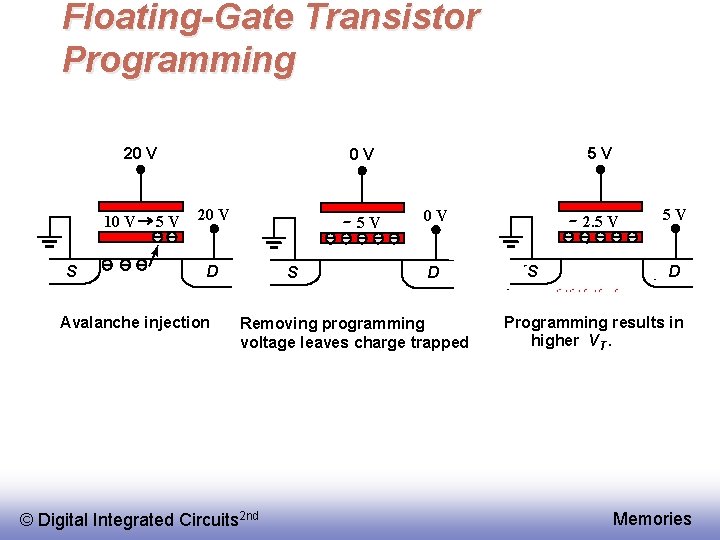
Floating-Gate Transistor Programming 20 V 10 V S 5 V 5 V 0 V 20 V - 5 V D Avalanche injection S D Removing programming voltage leaves charge trapped © Digital Integrated Circuits 2 nd - 2. 5 V 0 V S 5 V D Programming results in higher V T. Memories

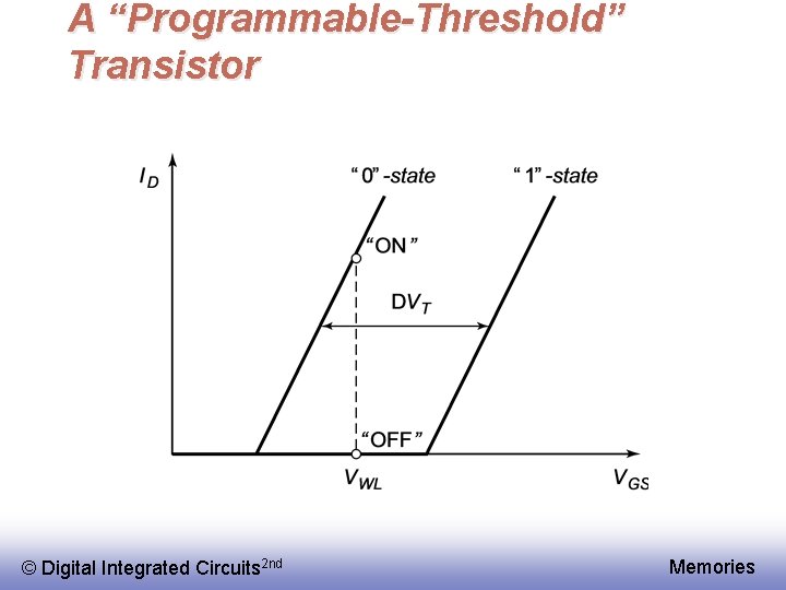
A “Programmable-Threshold” Transistor © Digital Integrated Circuits 2 nd Memories

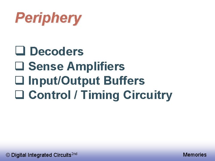
Periphery q Decoders q Sense Amplifiers q Input/Output Buffers q Control / Timing Circuitry © Digital Integrated Circuits 2 nd Memories

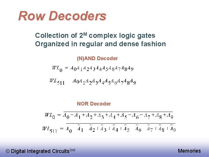
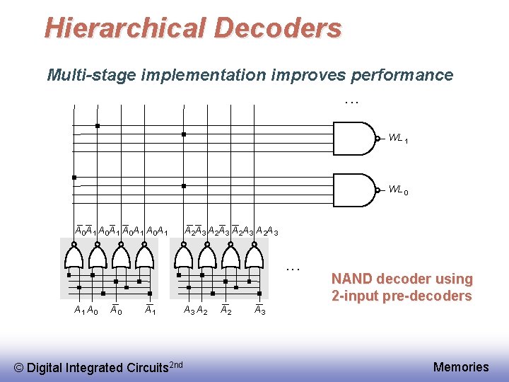
Row Decoders Collection of 2 M complex logic gates Organized in regular and dense fashion (N)AND Decoder NOR Decoder © Digital Integrated Circuits 2 nd Memories

Hierarchical Decoders Multi-stage implementation improves performance • • • WL 1 WL 0 A 0 A 1 A 2 A 3 • • • A 1 A 0 A 1 © Digital Integrated Circuits 2 nd A 3 A 2 A 3 NAND decoder using 2 -input pre-decoders Memories

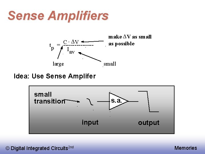
Sense Amplifiers × DV C tp = --------Iav large make D V as small as possible small Idea: Use Sense Amplifer small transition s. a. input © Digital Integrated Circuits 2 nd output Memories

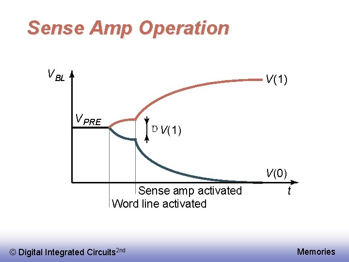
Sense Amp Operation V BL V(1) V PRE D V(1) V(0) Sense amp activated Word line activated © Digital Integrated Circuits 2 nd t Memories

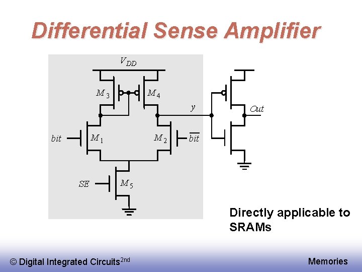
Differential Sense Amplifier V DD M 3 M 4 y M 1 bit SE M 2 Out bit M 5 Directly applicable to SRAMs © Digital Integrated Circuits 2 nd Memories

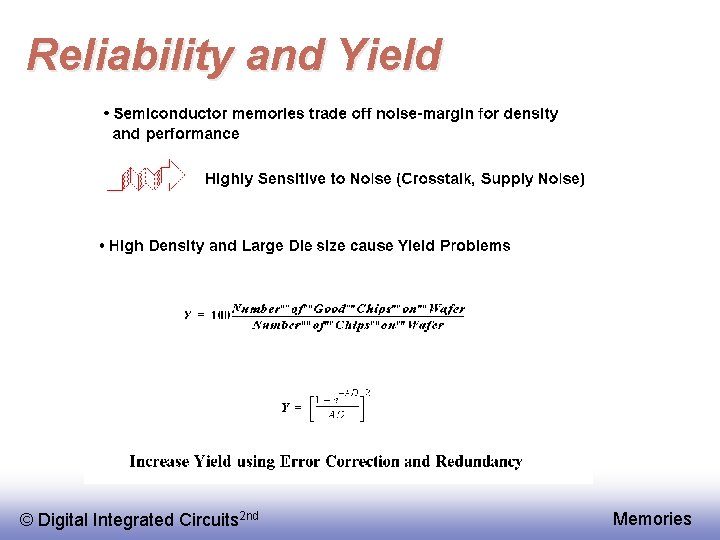
Reliability and Yield © Digital Integrated Circuits 2 nd Memories

References n Digital Integrated Circuits, 2 nd Edition, Jan Rabaey, Anantha Chandrakasan, Borivoje Nikolic Chapter 12 http: //bwrc. eecs. berkeley. edu/Ic. Book/slides. htm n Sedra & Smith, Microelectronic Circuits, 4 th Edition, Chapter 13 ¨ n Section 13. 9, 13. 10, 13. 11, 13. 12 VLSI Memory Chip Design, Kiyoo Itoh