Semiconductor Manufacturing Technology Michael Quirk Julian Serda October
Semiconductor Manufacturing Technology Michael Quirk & Julian Serda © October 2001 by Prentice Hall Chapter 12 Metallization Semiconductor Manufacturing Technology by Michael Quirk and Julian Serda © 2001 by Prentice Hall
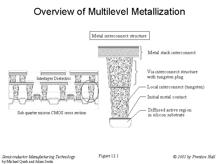
Overview of Multilevel Metallization Metal interconnect structure Metal stack interconnect Via interconnect structure with tungsten plug Interlayer Dielectric Local interconnect (tungsten) Initial metal contact Diffused active region in silicon substrate Sub quarter micron CMOS cross section Semiconductor Manufacturing Technology by Michael Quirk and Julian Serda Figure 12. 1 © 2001 by Prentice Hall
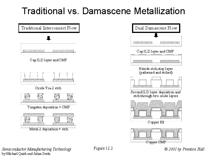
Traditional vs. Damascene Metallization Traditional Interconnect Flow Dual Damascene Flow Cap ILD layer and CMP Nitride etch-stop layer (patterned and etched) Oxide Via-2 etch Second ILD layer deposition and etch through two oxide layers Tungsten deposition + CMP Copper fill Metal-2 deposition + etch Copper CMP Semiconductor Manufacturing Technology by Michael Quirk and Julian Serda Figure 12. 2 © 2001 by Prentice Hall
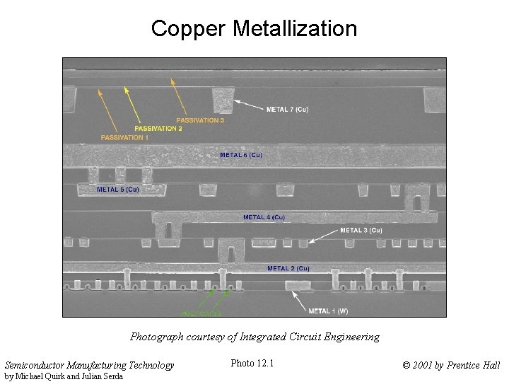
Copper Metallization Photograph courtesy of Integrated Circuit Engineering Semiconductor Manufacturing Technology by Michael Quirk and Julian Serda Photo 12. 1 © 2001 by Prentice Hall
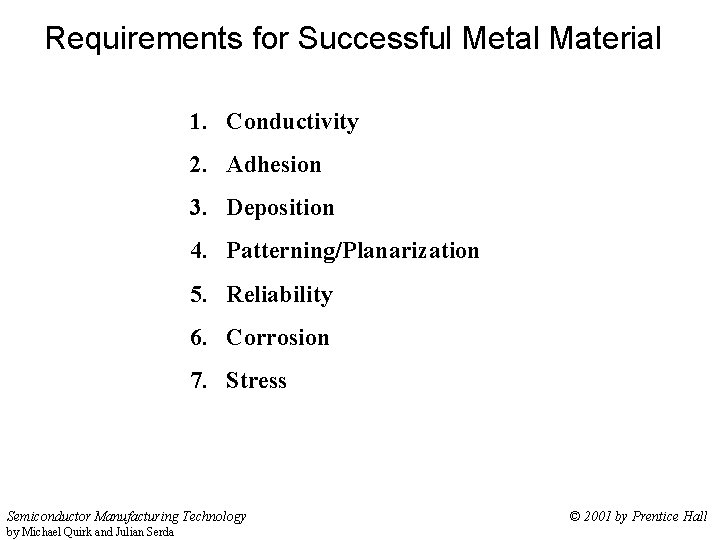
Requirements for Successful Metal Material 1. Conductivity 2. Adhesion 3. Deposition 4. Patterning/Planarization 5. Reliability 6. Corrosion 7. Stress Semiconductor Manufacturing Technology by Michael Quirk and Julian Serda © 2001 by Prentice Hall

Silicon and Select Wafer Fab Metals (at 20°C) Semiconductor Manufacturing Technology by Michael Quirk and Julian Serda Table 12. 1 © 2001 by Prentice Hall
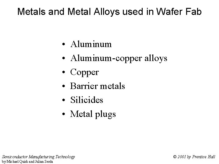
Metals and Metal Alloys used in Wafer Fab • • • Aluminum-copper alloys Copper Barrier metals Silicides Metal plugs Semiconductor Manufacturing Technology by Michael Quirk and Julian Serda © 2001 by Prentice Hall

Aluminum Interconnect Semiconductor Manufacturing Technology by Michael Quirk and Julian Serda Figure 12. 3 © 2001 by Prentice Hall
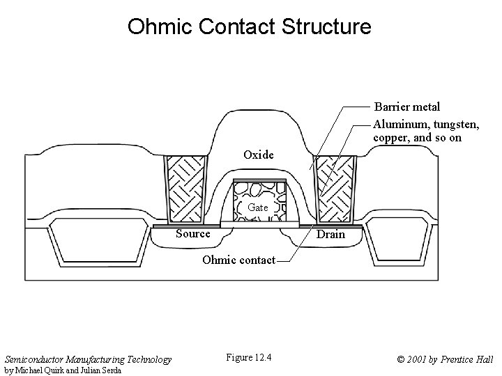
Ohmic Contact Structure Barrier metal Aluminum, tungsten, copper, and so on Oxide Gate Source Drain Ohmic contact Semiconductor Manufacturing Technology by Michael Quirk and Julian Serda Figure 12. 4 © 2001 by Prentice Hall

Junction Spiking Shallow junction Junction short Semiconductor Manufacturing Technology by Michael Quirk and Julian Serda Figure 12. 5 © 2001 by Prentice Hall

Hillock on a Metal Line due to Electromigration Hillocks short-circuit two metal lines Void in metal line Semiconductor Manufacturing Technology by Michael Quirk and Julian Serda Figure 12. 6 © 2001 by Prentice Hall

The Benefits of Copper Interconnect 1. Reduction in resistivity – 1. 678 W-cm vs. 2. 65 W-cm for Aluminum 2. Reduction in power consumption 3. Tighter packing density 4. Superior resistance to electromigration 5. Fewer process steps – 20 to 30 % fewer steps with damascene technique Semiconductor Manufacturing Technology by Michael Quirk and Julian Serda © 2001 by Prentice Hall

Change in Interconnect Delay Compared to 0. 25 - m Device Generation Semiconductor Manufacturing Technology by Michael Quirk and Julian Serda Table 12. 2 © 2001 by Prentice Hall

Comparison of Properties/Processes Between Al and Cu Semiconductor Manufacturing Technology by Michael Quirk and Julian Serda Table 12. 3 © 2001 by Prentice Hall

Three Major Challenges to Using Copper Interconnects in Semiconductor Products 1. Copper diffuses quickly into oxides and silicon. 2. Copper cannot be easily patterned using regular plasma etching techniques. 3. Copper oxidizes quickly in air at low temperatures (<200 C) and does not form a protective layer to stop further oxidation. Semiconductor Manufacturing Technology by Michael Quirk and Julian Serda © 2001 by Prentice Hall

Barrier Layer for Copper Interconnect Structure Barrier metal Copper Semiconductor Manufacturing Technology by Michael Quirk and Julian Serda Figure 12. 7 © 2001 by Prentice Hall

The Essential Properties of Barrier Metal 1. Good diffusion barrier properties so that the diffusivity of the two interface materials (e. g. , tungsten and silicon) is low at the sintering temperature (sintering refers to joining of the materials by thermal means). 2. High electrical conductivity with low ohmic contact resistance. 3. Good adhesion between the semiconductor and metal. 4. Resistance to electromigration. 5. Stability when thin and at high temperature. 6. Resistance to corrosion and oxidation. Semiconductor Manufacturing Technology by Michael Quirk and Julian Serda © 2001 by Prentice Hall

Ta for Copper Barrier Metal Tantalum Copper Semiconductor Manufacturing Technology by Michael Quirk and Julian Serda Figure 12. 8 © 2001 by Prentice Hall

Refractory Metal Silicide at a Silicon Contact Titanium silicide contact Polysilicon gate Oxide Titanium/titaniumnitride barrier metal Tungsten metal Drain Source Oxide Silicon substrate Titanium silicide contact Semiconductor Manufacturing Technology by Michael Quirk and Julian Serda Figure 12. 9 © 2001 by Prentice Hall

Some Properties of Select Silicides Semiconductor Manufacturing Technology by Michael Quirk and Julian Serda Table 12. 4 © 2001 by Prentice Hall

Polycide on Polysilicon Titanium polycide Polysilicon gate Titanium silicide Doped silicon Semiconductor Manufacturing Technology by Michael Quirk and Julian Serda Figure 12. 10 © 2001 by Prentice Hall

Anneal Phases of Ti. Si 2 Semiconductor Manufacturing Technology by Michael Quirk and Julian Serda Figure 12. 11 © 2001 by Prentice Hall

Chip Performance Issues Related to a Salicide Structure Reduced gate to S/D resistance Reduced sheet resistance Ti. Si 2 STI S Ti. Si 2 G D Reduced contact resistance Semiconductor Manufacturing Technology by Michael Quirk and Julian Serda Figure 12. 12 STI Reduced diode leakage © 2001 by Prentice Hall

Formation of Self-Aligned Metal Silicide (Salicide) Polysilicon Spacer oxide Field oxide Active silicon region Silicon substrate 1. Active silicon regions 2. Titanium deposition Titanium-silicon reaction regions 3. Rapid thermal anneal treatment Semiconductor Manufacturing Technology by Michael Quirk and Julian Serda Figure 12. 13 Ti. Si 2 formation 4. Titanium strip © 2001 by Prentice Hall

Tungsten Plug for Multilevel Metal Layers Aluminum contacts Oxide (dielectric) Early metallization technique 1. Contact etch through oxide 2. Aluminum deposition 3. Aluminum etch Semiconductor Manufacturing Technology by Michael Quirk and Julian Serda Tungsten plugs inside contact holes (vias) Oxide (dielectric) Current metallization technique 1. 2. 3. 4. 5. 6. Figure 12. 14 Thick oxide deposition Oxide planarization Contact etch through oxide Barrier metal deposition Tungsten planarization © 2001 by Prentice Hall

Metal Plugs in IC Si. O 2 Photograph courtesy of Integrated Circuit Engineering Semiconductor Manufacturing Technology by Michael Quirk and Julian Serda Photo 12. 2 © 2001 by Prentice Hall

Metal Deposition Systems Physical Vapor Deposition (PVD) • • Evaporation Sputtering Metal CVD Copper electroplating Semiconductor Manufacturing Technology by Michael Quirk and Julian Serda © 2001 by Prentice Hall

Simple Evaporator Wafer carrier Evaporating metal Crucible Process chamber (bell jar) Hi-Vac valve Roughing pump Hi-Vac pump Semiconductor Manufacturing Technology by Michael Quirk and Julian Serda Figure 12. 15 © 2001 by Prentice Hall

Some Advantages of Sputtering 1. Ability to deposit and maintain complex alloys. 2. Ability to deposit high-temperature and refractory metals. 3. Ability to deposit controlled, uniform films on large wafers (200 mm and larger). 4. Ability of multichamber cluster tools to clean the wafer surface for contamination and native oxides before depositing metal (referred to as in situ sputter etch). Semiconductor Manufacturing Technology by Michael Quirk and Julian Serda © 2001 by Prentice Hall

Simple Parallel Plate DC Diode Sputtering System Cathode (-) 1) Electric fields create Ar+ ions. + + + Metal target Ar+ 2) High-energy ions collide with metal target. e- Gas delivery Argon atoms e- Plasma Electric field e 3) Metallic atoms are dislodged from target. 4) Metal atoms migrate toward substrate. Exhaust 6) Excess matter is removed from chamber by a vacuum pump. DC diode sputterer 5) Metal deposits on substrate Substrate Anode (+) Semiconductor Manufacturing Technology by Michael Quirk and Julian Serda Figure 12. 16 © 2001 by Prentice Hall

Dislodging Metal Atoms from Surface of Sputtering Target Cathode (-) Metal atoms Sputtered metal atom by Michael Quirk and Julian Serda 0 Semiconductor Manufacturing Technology + High-energy Ar+ ion Figure 12. 17 Rebounding argon ion recombines with free electron to form a neutral atom. © 2001 by Prentice Hall

Factors that Affect Sputter Yield 1. Incident angle of the bombarding ions. 2. Composition and geometry of the target material. 3. Mass of bombarding ions. 4. Energy of the bombarding ions. Semiconductor Manufacturing Technology by Michael Quirk and Julian Serda © 2001 by Prentice Hall

Different Species Landing on Substrate Cathode (-) Metal target Photons from plasma glow X-rays from target bombardment High energy electrons e- Electric field - Ions including impurities Neutrals – - Ions Sputtered atoms Substrate Anode (+) Semiconductor Manufacturing Technology by Michael Quirk and Julian Serda Figure 12. 18 © 2001 by Prentice Hall

Three Types of Sputtering Systems • RF (radio frequency) • Magnetron • IMP (ionized metal plasma) Semiconductor Manufacturing Technology by Michael Quirk and Julian Serda © 2001 by Prentice Hall

RF Sputtering System Matching network Blocking capacitor Electrode RF generator Microcontroller operator interface Gas flow controller Target Substrate Pressure controller Gas panel Chuck Turbo pump Exhaust Roughing pump Argon Semiconductor Manufacturing Technology by Michael Quirk and Julian Serda Figure 12. 19 © 2001 by Prentice Hall

Magnetron Sputtering DC power supply Magnet Argon inlet Cathode Target Heated wafer chuck Vacuum Pump Semiconductor Manufacturing Technology by Michael Quirk and Julian Serda Figure 12. 20 © 2001 by Prentice Hall

Collimated Sputtering System Target Ar Cross section of via showing coverage of resulting sputtered film. Collimator Semiconductor Manufacturing Technology by Michael Quirk and Julian Serda Figure 12. 21 © 2001 by Prentice Hall

Concept of Ionized Metal Plasma PVD DC supply Electrode Titanium target High-energy Ar+ ion + e- Sputtered Ti atom Plasma Induction coil DC field e- RF field + Ti+ ion Substrate Electrode DC bias supply Semiconductor Manufacturing Technology by Michael Quirk and Julian Serda RF generator Figure 12. 22 © 2001 by Prentice Hall

Metal CVD • Tungsten CVD – Excellent step coverage and gap fill – High electromigration resistance • Copper CVD – Excellent conformality Semiconductor Manufacturing Technology by Michael Quirk and Julian Serda © 2001 by Prentice Hall

Blanket Tungsten CVD with Ti/Ti. N Barrier Metal Ti Via PECVD Si. O 2 Gap fill dielectric Aluminum 1. Interlayer dielectric via etch 2. Collimated Ti deposition covers bottom of via Ti. N Tungsten plug Tungste n via fill 3. CVD Ti. N conformal deposition Semiconductor Manufacturing Technology by Michael Quirk and Julian Serda 4. CVD tungsten deposition Figure 12. 23 5. Tungsten planarization © 2001 by Prentice Hall

PVD Cluster Tool Photo Courtesy of Applied Materials, Inc. Semiconductor Manufacturing Technology by Michael Quirk and Julian Serda Photo 12. 3 © 2001 by Prentice Hall

Copper Electroplating - Cathode Outlet Copper atom attached to wafer Copper + ion Substrate Plating solution + + Copper anode Inlet Semiconductor Manufacturing Technology by Michael Quirk and Julian Serda Figure 12. 24 © 2001 by Prentice Hall

Electroplating Tool Used with permission from Novellus Systems, Inc. Semiconductor Manufacturing Technology by Michael Quirk and Julian Serda Photo 12. 4 © 2001 by Prentice Hall

Traditional Aluminum Structure Si. O 2 Photograph courtesy of Integrated Circuit Engineering Semiconductor Manufacturing Technology by Michael Quirk and Julian Serda Photo 12. 4 © 2001 by Prentice Hall
![Table 12. 5. 1 [55] Copper Metallization using Dual Damascene Process Step: Si. O Table 12. 5. 1 [55] Copper Metallization using Dual Damascene Process Step: Si. O](http://slidetodoc.com/presentation_image_h2/b3009341876bb715b4a006de8f9fce32/image-45.jpg)
Table 12. 5. 1 [55] Copper Metallization using Dual Damascene Process Step: Si. O 2 deposition Si. O 2 Description: . ILD oxide deposition with PECVD to desired thickness for via There is no critical gap fill therefore PECVD is acceptable. Semiconductor Manufacturing Technology by Michael Quirk and Julian Serda Table 12. 5. 1 © 2001 by Prentice Hall

Table 12. 5. 2 Copper Metallization using Dual Damascene Process Step: Si. N etch stop deposition Si. N Description: Thin (250 Å) Si. N etch stop is deposited on ILD oxide. The Si. N needs to be dense and pinholefree; therefore HDPCVD is used. Semiconductor Manufacturing Technology by Michael Quirk and Julian Serda Table 12. 5. 2 © 2001 by Prentice Hall

Table 12. 5. 3 Copper Metallization using Dual Damascene Process Step: Via patterning and etch Si. N Description: Photolithography to pattern and dry etch via openings into Si. N. Strip photoresist after completion of etch. Semiconductor Manufacturing Technology by Michael Quirk and Julian Serda Table 12. 5. 3 © 2001 by Prentice Hall

Table 12. 5. 4 Copper Metallization using Dual Damascene Process Step: Deposit remaining Si. O 2 Description: PECVD oxide deposition for remaining ILD oxide. Semiconductor Manufacturing Technology by Michael Quirk and Julian Serda Table 12. 5. 4 © 2001 by Prentice Hall

Table 12. 5. 5 Copper Metallization using Dual Damascene Process Step: Interconnect patterning Photoresist Description: Photolithography to pattern Si. O 2 trench with resist. Previously patterned via openings are located in trench. Semiconductor Manufacturing Technology by Michael Quirk and Julian Serda Table 12. 5. 5 © 2001 by Prentice Hall

Table 12. 5. 6 Copper Metallization using Dual Damascene Process Step: Etch trench for interconnect and hole for via Description: Dry etch trench in ILD oxide, stopping on the Si. N layer. Etch continues to form via opening by passing through opening in Si. N. Semiconductor Manufacturing Technology by Michael Quirk and Julian Serda Table 12. 5. 6 © 2001 by Prentice Hall

Table 12. 5. 7 Copper Metallization using Dual Damascene Process Step: Deposit Barrier Metal Barrier metal Description: Deposit Ta or Ta. N diffusion layer with ionized PVD on bottom and sidewalls of trench and via. Semiconductor Manufacturing Technology by Michael Quirk and Julian Serda Table 12. 5. 7 © 2001 by Prentice Hall

Table 12. 5. 8 Copper Metallization using Dual Damascene Process Step: Deposit Cu seed layer Description: Deposit continuous Cu seed layer with CVD. The layer must be uniform and free of pinholes Semiconductor Manufacturing Technology by Michael Quirk and Julian Serda Table 12. 5. 8 © 2001 by Prentice Hall

Table 12. 5. 9 Copper Metallization using Dual Damascene Process Step: Deposit Cu fill Copper layer Description: Deposit Cu fill with electrochemical deposition (ECD). Fill both via opening and trench. Semiconductor Manufacturing Technology by Michael Quirk and Julian Serda Table 12. 5. 9 © 2001 by Prentice Hall

Table 12. 5. 10 Copper Metallization using Dual Damascene Process Step: Remove excess Cu with Copper Description: CMP remove excess Cu using chemical mechanical planarization (CMP). This planarizes the surface and prepares for next level. The resulting surface is a planar structure with metal inlays in the dielectric to form the circuitry. Semiconductor Manufacturing Technology by Michael Quirk and Julian Serda Table 12. 5. 10 © 2001 by Prentice Hall
- Slides: 54