Semiconductor Manufacturing Technology Chapter 16 Etch Objectives After

Semiconductor Manufacturing Technology Chapter 16 Etch

Objectives After studying the material in this chapter, you will be able to: 1. List and discuss eight important etch parameters. 2. Explain dry etch, including its advantages and how etching action takes place. 3. List and describe the equipment systems for seven dry plasma etch reactors. 4. Explain the benefits of high-density plasma (HDP) etch and the discuss the four types of HDP reactors. 5. Give an application example for dielectric, silicon and metal dry etch. 6. Discuss wet etch and its applications. 7. Explain how photoresist is removed. 8. Discuss etch inspection and important quality measures.

Applications for Wafer Etch in CMOS Technology 통상적으로 포토 레지스터가 있는 상태에서 식각을 수행한다. Photoresist mask Film to be etched (a) Photoresist-patterned substrate Photoresist mask Protected film (b) Substrate after etch 그림에서 식각된 물질 아래에 있는 물질은 왜 식각되지 않는가? Figure 16. 1
 Wafer start Thin Films Polish")
Process Flow in a Wafer Fab Wafer fabrication (front-end) Wafer start Thin Films Polish Photo Etch Unpatterned wafer Completed wafer Test/Sort Diffusion Implant Used with permission from Advanced Micro Devices Figure 16. 2

Etch Process Categories of Etch Processes • Wet Etch • Dry Etch • Three Major Materials to be Etched – Silicon – Dielectric – Metal • Patterned Etch Versus Unpatterned Etch 무슨 뜻?
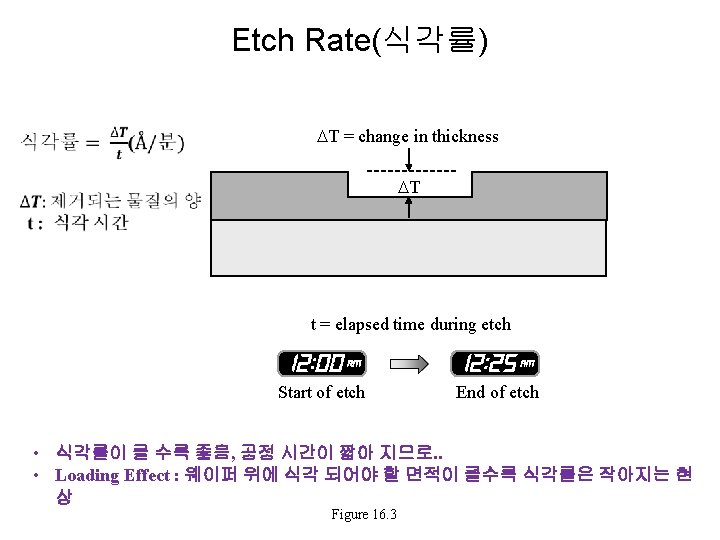
 Etch rate Etch")
Page 535~541 읽어 보세요 • • • Etch Parameters (매우 중요) Etch rate Etch profile Etch bias Selectivity Uniformity Residues Polymer formation Plasma-induced damage Particle contamination and defects
 모양이 왜 이렇지? Isotropic etch - etches in")
Wet Chemical Isotropic Etch (등방성 식각) 모양이 왜 이렇지? Isotropic etch - etches in all directions at the same rate Resist Film Substrate 좋은 것인가? Figure 16. 4
 Anisotropic etch - etches in only")
Anisotropic Etch with Vertical Etch Profile (이방성 식각) Anisotropic etch - etches in only one direction Resist Film Substrate Resist는 전혀 식각이 안되나? Figure 16. 5

Sidewall Profiles for Wet Etch Versus Dry Etch의 Etch Profile이 왜 이리 다양하지? Table 16. 1

Etch Bias 왼쪽 그림과 오른쪽 그림의 차이를 이해하시나요? Wb Wa Bias Resist Film Substrate (a) (b) Figure 16. 6

Etching Undercut and Slope Undercut Resist Overetch Film Substrate 궁금한 거 없으시나요? Figure 16. 7
 무슨 뜻? Randomly select 3 to 5 wafers in a lot")
Etch Uniformity (균일성) 무슨 뜻? Randomly select 3 to 5 wafers in a lot Measure etch rate at 5 to 9 locations on each wafer, then calculate etch uniformity for each wafer and compare wafer-to-wafer. 색깔 칠한 부분은 ? Uniformity 측정은 Wafer내에서, Wafer to Figure 16. 9 Wafer, Lot to Lot 평가한다.
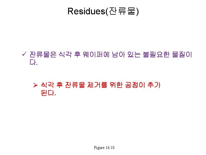

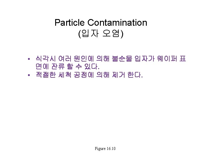
Polymer Sidewall Passivation for Increased Anisotropy 식각 후 polymer 제거를 위한 공정이 추가 된다. Plasma ions Resist Oxide Silicon Polymer formation Polymer는 의도적으로 측면 식각을 방지하기 위해 증착된다. . Figure 16. 10

Dry Etch • Advantages of Dry Etch over Wet Etch • Etching Action • Potential Distribution

Advantages of Dry Etch over Wet Etch Page 541 표 16 -2 읽어 보세요 Table 16. 2
 Etchant gases enter")
Plasma Etch Process of a Silicon Wafer RF generator Anode 1) Etchant gases enter chamber Electric field Etch process chamber Gas delivery By-products l 2) Dissociation of reactants by electric fields 4) Reactive +ions bombard surface Anisotropic etch 8) By-product removal 3) Recombination of electrons with atoms creates plasma Exhaust l 5) Adsorption of reactive ions on surface 6) Surface reactions of 7) Desorption of radicals and surface film by-products Isotropic etch Substrate Cathode 번호 순서대로 공정이 진행된다. Figure 16. 11

Chemical and Physical Dry Etch Mechanisms Physical Etching Chemical Etching Sputtered surface material Reactive +ions bombard surface Desorption of by-products Surface reactions of radicals + surface film Isotropic etch Anisotropic etch 이방성 등방성 Figure 16. 12

Page 544 표 16 -4 읽어 보세요 Chemical Versus Physical Dry Plasma Etching Table 16. 3
 Ion")
Schematic View of Reactor Glow Discharge with Potential Distribution RF Powered electrode (Vt) Ion sheath Plasma (+Vp) -V 0 +V Vt Vp Grounded electrode Figure 16. 13
 Table 16. 4")
Effects of Changing Plasma Etch Parameters (플라즈마 식각시 공정 변수들) Table 16. 4
 reactor Downstream")
Plasma Etch Reactors • • • Barrel plasma etcher Parallel plate (planar) reactor Downstream etch systems Triode planar reactor Ion beam milling Reactive ion etch (RIE) High-density plasma etchers Etch System Review Endpoint Detection Vacuum for Etch Chambers
 Reactor Configuration Gas in Wafers Reaction chamber RF electrode RF generator Wafers")
Typical Barrel(원통형) Reactor Configuration Gas in Wafers Reaction chamber RF electrode RF generator Wafers Quartz boat Vacuum pump 0. 1 ~1 torr 기압, 등방성 식각, 통상적으로 wafer에서 PR을 제거 할 때 사용 Figure 16. 14

Parallel Plate Plasma Etching Matching network RF generator Gas dispersion screen Microcontroller Operator Interface Gas- flow controller Endpoint signal Wafer Pressure controller Pressure signal Gas panel Electrodes Exhaust Roots pump Roughing pump Process gases Figure 16. 15

Schematic of a Downstream Reactor Microwave source 2. 45 MHz Microwave energy 이온 충격으로 부터 Wafer를 보호하기 위해 플라즈마가 아랫방향으로 흐르도록 제작. 등방성 식각, 화학적 식각 Plasma chamber Diffuser Wafer chuck Heat lamp To vacuum system Figure 16. 16
 Capacitor Capacitively-coupled RF")
Triode Planar Reactor Induction coil Inductively-coupled RF generator (3. 56 MHz) Capacitor Capacitively-coupled RF generator (100 k. Hz) 이온 충돌량을 통제하기 위해 3극으로 만듬 단일 결정 Si을 식각시 사용. Figure 16. 17

General Schematic of Ion Beam Etcher Screen grid Electromagnet improves ionization + _ Accelerating grid Neutralizing filament + Plasma chamber (+anode repels +ions) Hot filament emits electrons Gas inlet (Argon) 이온 빔 식각은 금이나 백금, 그리고 구리와 같이 식각하기 어려운 물질을 식각 할 때 사 용 + + + + + + ++ + + + + + + + Wafer can be tilted to control etch profile To vacuum system Redrawn from Advanced Semiconductor Fabrication Handbook, Integrated Circuit Engineering Corp. , p. 8 -12. Figure 16. 18
 반응성 화학 공정과 물리적 공정을 이용하 여")
Parallel Plate RIE Reactor Grounded electrode (anode) 반응성 화학 공정과 물리적 공정을 이용하 여 물질을 식각한다. Powered electrode (cathode) F Ar+ (chemical etch component) (physical etch component) RF generator Figure 16. 19 Wafer

High Density Plasma Etcher 낮은 압력에서 고밀도 플라즈마를 발생시켜 높은 식각률을 유도한 다. Photograph courtesy of Applied Materials, Metal Etch DPS Photo 16. 1

Schematic of Electron Cyclotron Reactor Microwave source 2. 45 MHz Quartz window Wave guide Plasma chamber Diffuser 고밀도 플라즈마 장비의 일종 Cyclotron magnet Wafer Additional magnet 13. 56 MHz Electrostatic chuck Vacuum system Redrawn from Y. Lii, “Etching, ” ULSI Technology, ed. by C. Chang & S. Sze, (New York: Mc. Graw-Hill, 1996), p. 349. Figure 16. 20

Inductively Coupled Plasma Etch Inductive coil RF generator 고밀도 플라즈마 장비의 일종 Dielectric window Plasma chamber Biased wafer chuck Electromagnet Bias RF generator Redrawn from Y. Lii, “Etching, ” ULSI Technology, ed. By C. Chang and S. Sze (New York: Mc. Graw-Hill, 1996), p. 351. Figure 16. 21
 Inductively-coupled RF generator (source power) Decoupled plasma chamber Wafer Turbo")
Dual Plasma Source (DPS) Inductively-coupled RF generator (source power) Decoupled plasma chamber Wafer Turbo pump Cathode Lower chamber Capacitively-coupled RF generator (bias power) Redrawn from Y. Ye et al, Proceedings of Plasma Processing XI, vol. 96 -12, ed. by G. Mathad and M. Meyyappan (Pennington, NJ: The Electrochemical Society, 1996), p. 222. Figure 16. 22
 Electromagnet (1 of 4) Wafer Biased wafer chuck")
Magnetically Enhanced Reactive Ion Etch (MERIE) Electromagnet (1 of 4) Wafer Biased wafer chuck 13. 56 MHz Redrawn from Wet/Dry Etch (College Station, TX: Texas Engineering Extension Service, 1996), p. 165. Figure 16. 23

Dry Etcher Configurations Table 16. 5

Endpoint Detection for Plasma Etching Etch Parameter 종료점 검출은 우리가 원하는 물질만 제거 하고 식각을 멈추는 것을 알려주는 것이다. Endpoint detection Normal etch Change in etch rate detection occurs here. Endpoint signal stops the etch. Time 종료점 검출은 식각률의 변화나 식각 후 생성되는 부산물로부터 측정한다. Figure 16. 24
")
Characteristic Wavelengths of Excited Species in Plasma Etch 광학 방사 분광학 (Optical Emission Spectroscopy) : 여기되는 입자들은 특정한 재료에 해당하는 파장의 빛을 방출하 고 이를 분석하여 종료점 검출을 진행한다. Table 16. 6

Endpoint Detection Photograph courtesy of Advanced Micro Devices, Lam Rainbow etcher

Dry Etch Applications • Dielectric Dry Etch – Oxide – Silicon Nitride • Silicon Dry Etch – Polysilicon – Single-Crystal Silicon • Metal Dry Etch – Aluminum and Metal Stacks – Tungsten Etchback – Contact Metal Etch
 Page 557 하단부분 읽어 보세요 1. High selectivity")
Requirements for Successful Dry Etch (중요함) Page 557 하단부분 읽어 보세요 1. High selectivity to avoid etching materials that are not to be etched (primarily photoresist and underlying materials). 2. Fast etch rate to achieve an acceptable throughput of wafers. 3. Good sidewall profile control. 4. Good etch uniformity across the wafer. 5. Low device damage. 6. Wide process latitude for manufacturing.

Dry Etch Critical Parameters Page 558 상단 부분 읽어 보세요 Equipment Parameters: • • Equipment design Source power Source frequency Pressure Temperature Gas-flow rate Vacuum conditions Process recipe Process Parameters: • Plasma-etching a wafer • • Other Contributing Factors: • • Cleanroom protocol Operating procedures Maintenance procedures Preventive maintenance schedule 장비 하나에 생각해야 하고 알아야 할 것이 무척 많죠? Figure 16. 25 Plasma-surface interaction: - Surface material - Material stack of different layers - Surface temperature - Surface charge - Surface topography Chemical and physical requirements Time Quality Measures: • • • Etch rate Selectivity Uniformity Feature profile Critical dimensions Residue

Oxide Etch Reactor CF 4 C 3 F 8 Selection of fluorocarbon and hydrocarbon chemicals C 4 F 8 CHF 3 NF 3 Si. F 4 Ar CHF HF Plasma F Electrostatic chuck 높은 Aspect ratio, 높은 선택도가 요구됨. 탄화불소 화합물 이용 Figure 16. 26 CF 2 CH 4 Wafer

Etch Stop Hard Mask Layer Example: Silicon nitride, Si 3 N 4, serves as etch-stop during LI oxide etch. Note: The numbers show the order of the five operations. Nitride를 사용하여 선택도를 높이기도 한다. Nitride와 Oxide의 선택비가 매 우 높기 때문에 가능한 일이다. Figure 16. 27

Contact Etching to Varying Depths Contact holes G S D Figure 16. 28

Polysilicon Conductor Length Polysilicon gate Gate oxide Gate Oxide 층이 매 우 얇기 때문에 높은 선택도가 필요하다. 또한 균일성 및 반복 성도 우수해야 한다. Gate Source Drain The gate length determines channel length and defines boundaries for source and drain electrodes. Figure 16. 29

Polysilicon Gate Etch Process Steps Page 563 상단부분 읽어 보세요 1. Breakthrough step to remove native oxide and surface contaminants 2. Main-etch step to remove most polysilicon without damage to gate oxide 3. Overetch step to remove remaining residues and poly stringers while maintaining high selectivity to gate oxide

Undesirable Microtrenching during Polysilicon Gate Etching Ions 왜 그럴까요? Resist Trench in gate oxide Poly Gate oxide Substrate 메인 식각에서 150 : 1 잔류물 식각에서 250 : 1 의 선택도 필요 Figure 16. 30

Silicon Trench Etching 어떤 어려움이 있나요? Figure 16. 31

Major Requirements for Metal Etching Page 565 중간부분 읽어 보세요 1. High etch rates (>1000 nm/min). 2. High selectivity to the masking layer (>4: 1), interlayer dielectric (>20: 1) and to underlying layers. 3. High uniformity with excellent CD control and no microloading (<8% at any location on the wafer). 4. No device damage from plasma-induced electrical charging. 5. Low residue contamination (e. g. , copper residue, developer attack and surface defects). 6. Fast resist strip, often in a dedicated cluster tool chamber, with no residual contamination. 7. No corrosion.

Metal Stack for VLSI/ULSI Integration Figure 16. 32

Typical Steps for Etching Metal Stacks Page 566 중간부분 읽어 보세요 1. 2. 3. 4. Breakthrough step to remove native oxide. ARC layer etch (may be combined with above step). Main etch step of aluminum. Overetch step to remove residue. It may be a continuation of the main etch step. 5. Barrier layer etch. 6. Optional residue removal process to prevent corrosion. 7. Resist removal.

W은 주로 접촉 구멍 메우는 데 사용함 Tungsten Etchback Si. O 2 Via Tungsten ILD-2 Metal-1 stack ILD-1 (a) Via etch through ILD-2 (Si. O 2) (b) Tungsten CVD via fill Si. O 2 Tungsten plug Metal-2 stack Tungsten plug (c) Tungsten etchback (d) Metal-2 deposition Etchback이 무엇인지 알겠죠!!!! Figure 16. 33
 • Wet Etch Parameters • Types of Wet Etch – Wet")
Wet Etch(습식 식각) • Wet Etch Parameters • Types of Wet Etch – Wet Oxide Etch – Wet Chemical Strips

P 569 표 16 -7 보세요 Wet Etch Parameters Table 16. 7

Approximate Oxide Etch Rates in BHF Solution at 25° C Table 16. 8

Historical Perspective Polysilicon Etch Technology Evolution Table 16. 9

Photoresist Removal Plasma Ashing • Asher Overview • Plasma Damage • Residue Removal
 O 2 molecules enter")
Atomic Oxygen Reaction with Resist in Asher Downstream Plasma 1) O 2 molecules enter chamber Asher reaction chamber Gas delivery 6) By-product removal l + + Neutral oxygen radicals + 2) O 2 dissociates into atomic oxygen l + + + 3) Plasma energy turns oxygen into + ions Figure 16. 34 5) By-product desorption 4) Neutral O and O+ react with C and H atoms in resist Resist Substrate Exhaust

Post Etch Via Veil Residue Polymer residue Via veils Figure 16. 35

Chapter 16 Review • Page 575 : 식각 검사의 품질 측정 • Page 576 : 건식 식각의 문제점 해결 (Troubleshooting)

Chapter 16 Review • • Quality Measures Troubleshooting Summary Key Terms Review Questions Equipment Suppliers’ Web Sites References 469 440 471 472 473 474
- Slides: 64