Semiconductor Manufacturing Technology Chapter 15 Photolithography Resist Development


 • Deep UV Exposure Bake – Temperature Uniformity – PEB Delay")


 formation Developer dispenser (a) Puddle dispense (b) Spin-off excess developer")
 Page 515~517 읽어 보세요. • • Developer Temperature Developer Time")


 – SCALPEL – Ion")


 Electron beam Step-and-scan")
")


 1970 s 10")
 Post exposure bake")

- Slides: 30
Semiconductor Manufacturing Technology Chapter 15 Photolithography: Resist Development and Advanced Lithography
Objectives After studying the material in this chapter, you will be able to: 1. Explain why and how a post exposure bake is done for conventional and Chemically amplified DUV resist. 2. Describe the negative and positive resist development process for conventional and chemically amplified DUV resist. 3. List and discuss the two most common resist development methods and the critical development parameters. 4. State why a hard bake is done after resist development. 5. Explain the benefits of a post-develop inspection. 6. List and describe the four different alternatives for advanced lithography, including the challenges for introducing each alternative into production. 7. Describe and give the benefit for the advanced resist process of top surface imaging.
Eight Basic Steps of Photolithography Development 란 무엇인가? Table 15. 1
Post Exposure Bake(PEB) • Deep UV Exposure Bake – Temperature Uniformity – PEB Delay • Conventional I-Line PEB의 역할 : 열처리에 의해 산을 발생시키고 산이 보호 그룹을 제거하게 되어 후속 현상 용액에서 용 해되도록 한다.
Amine Contamination of DUV Resist leading to “T-top” Formation PAG : Photoacid generator Region of unexposed photoresist Neutralized photoresist } PAG H+ Resist T-topping H+ PAG H+ Development PAG H+ H+ PAG Acid-catalyzed reaction of exposed resist (post PEB) H+ 빛을 쬐어 주고 development 공정 이 Figure 15. 1 지연되면 오염되어 T-shape이 된다.
Reduction of Standing Wave Effect due to PEB Standing waves Standing wave 효과 에 의해 매끄럽지 않는 현상이 발생하 는데 PEB를 진행하 면 PAC의 diffusion 에 의해 패턴을 매 끄럽게 해준다. PAC PAC PAC PAC PAC PAC (a) Exposure to UV light PAC PAC PAC PAC (b) Striations in resist PAC PAC diffusion PAC PAC PAC Exposed photoresist PAC PAC Unexposed photoresist PAC (c) PEB causes PAC diffusion Figure 15. 2 (d) Result of PEB
Develop • • Negative Resist Positive Resist Development Methods Resist Development Parameters
Photoresist Development Problems X로 표시된 패턴에는 무슨 문제가 있는가? Resist Substrate X X Ö X Under develop Incomplete develop Correct develop Severe overdevelop Figure 15. 3
Negative Resist Crosslinking Negative Resist는 작은 크기의 패턴을 형성하는 데는 적합 하지 않다. UV Exposed resist Crosslinks Unexposed resist 빛을 받은 부분이 남고 빛을 안받은 부분이 제거된다. Figure 15. 4
Development of Positive Resist exposed to light dissolves in the develop chemical. Unexposed positive resist 미세 패턴 형성시 사용한다. Crosslinked resist 빛을 받은 부분이 제거되고 빛을 안받은 부분이 남는다. Figure 15. 5
Development Methods • Continuous Spray Development • Puddle Development
Resist Development with Continuous Spray Load Station Vapor Prime Resist Coat Spray Develop. Rinse Edge-bead Removal Transfer Station Wafer Transfer System To vacuum pump Soft Bake Cool Plate Hard Bake (a) Wafer track system Vacuum chuck Spindle connected to spin motor (b) Developer spray dispenser Figure 15. 6
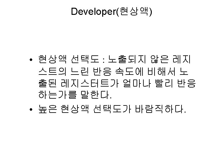
Puddle Resist Development Puddle(물웅덩이) formation Developer dispenser (a) Puddle dispense (b) Spin-off excess developer (c) DI H 2 O rinse (d) Spin dry Figure 15. 7
Resist Development Parameters (중요함) Page 515~517 읽어 보세요. • • Developer Temperature Developer Time Developer Volume Normality Rinse Exhaust Flow Wafer Chuck
Hard Bake • Characteristics of Hard Bake: – Post-Development Exposure – Evaporates Residual Solvent in Photoresist – Hardens the Resist – Improves Resist-to-Wafer Adhesion – Prepares Resist for Subsequent Processing – Higher Temperature than Soft Bake, but not to Point Where Resist Softens and Flows • Resist Hardening with Deep UV
Softened Resist Flow at High Temperature 너무 높은 온도에서 굽게 되면 포 토레지스터가 흐르게 되어 패턴 이 무너진다. Photoresist Figure 15. 8
Develop Inspect • • Post-Develop Inspection to Find Defects before Etching or Implanting Prevents Scrap Characterizes the Photo Process by Providing Feedback Regarding Quality of the Lithography Process • Develop Inspect Rework Flow
Automated Inspection Tool for Develop Inspect Photograph courtesy of Advanced Micro Devices, Leica Auto Inspection station Photo 15. 1
Develop Inspect Rework Flow UV light HMDS 1. Vapor prime O 2 Mask Resist 2. Spin coat 3. Soft bake 4. Align and expose 5. Post-exposure bake No Rejected wafers Plasma Strip and clean 7. Hard bake 8. Develop inspect Rework Yes Ion implant Passed wafers Etch 포토리소그래피 공정은 Rework이 가능한 공정이다. Figure 15. 9 6. Develop
Advanced Lithography • Next Generation Lithography – Extreme UV (EUV) – SCALPEL – Ion Projection Lithography (IPL) – X-Ray • Advanced Resist Processing – Development Trends of Photoresist and Lithography – DESIRE Process
Photolithography Improvements Page 519 하단을 읽어 보세요 Table 15. 2
Concept for Extreme Ultraviolet Lithography 13 nm의 UV 파장을 사용하여 30 nm 이하의 이미지를 패턴화 한다. Step-and-scan 4× reflection reticle High power laser Multilayer coated mirrors EUV ¼ image of reticle Plasma Target material Vacuum chamber Step-and-scan wafer stage Redrawn from International SEMATECH's Next Generation Lithography Workshop Brochure Figure 15. 10
Concept of SCALPEL SCattering with Angular Limitation Projection Electron Beam Lithography) Electron beam Step-and-scan reticle stage 광원 대신에 안정된 전자빔 소스를 사용한 다. 직접적으로 패턴을 웨 이퍼위에 그린다. Electrostatic lens system (4: 1 reduction) Step-and-scan wafer stage Vacuum chamber Redrawn from International SEMATECH's Next Generation Lithography Workshop Brochure Figure 15. 11
Ion Projection Lithography Ion source Ion beam Mask Electrostatic lens system (4: 1 reduction) Reference plate Step-and-scan wafer stage Vacuum chamber Redrawn from International SEMATECH's Next Generation Lithography Workshop Brochure Figure 15. 12
X-ray Spectrum Hard X-rays UV Spectrum Soft X-rays EUV 0. 1 nm 10 nm Synchrotron source Figure 15. 13 Excimer laser DUV MUV 100 nm Hg lamp
Concept of X-ray Photomask Gold plated chrome pattern X-ray absorbers Silicon wafer Glass frame Window etched into lower membrane Membrane X- ray s Scanning X-rays are directed toward a production wafer through a photomask similar to this one. Redrawn from C. Y. Chang and S. M. Sze, ULSI Technology, edited by C. Y. Chang and S. M. Sze (New York: Mc. Graw-Hill 1996) p. 314 Figure 15. 14
Development Trends of Photoresist and Lithography Negative photoresist Positive photoresist (DNQ-Novolak) 1970 s 10 mm 1. 2 mm 1980 s 1 mm 0. 40 mm Chemical amplification 1990 s 0. 35 mm Contact Printer Scanning Aligner G-line Stepper I-line Stepper PSM, OAI 장치 DUV Stepper 0. 18 mm DUV Step and Scan EUV Step and Scan Advanced photoresist top surface imaging 2000 s 0. 13 mm 0. 1 mm 2010 Figure 15. 15 SCALPEL IPL, X-ray 광원
Top Surface Imaging UV Exposed resist Exposed Crosslinked Unexposed resist (b) Post exposure bake (a) Normal exposure process HMDS Si Si Silylated exposed resist (c) Vapor phase silyation O 2 plasma develop (d) Final developed pattern Figure 15. 16
Chapter 15 Review • • Quality Measures Troubleshooting Summary Key Terms Review Questions Equipment Suppliers’ Web Sites References 429 431 432 433 433 434