Semiconductor Manufacturing Technology Chapter 14 Photolithography Alignment and


 STI etch 2) P-well implant 3) N-well")


 Constructive Destructive A Waves in phase Waves out of phase B")
 Broadband light Reflected wavelengths Coating 1 (non-reflecting) Secondary reflections (interference) Coating")
 Visible spectrum Ultraviolet spectrum EUV 4 13 50 VUV 100 150")


 Sloping profile Substrate 레지스트 바닥과")


 Refraction of Light(빛의 굴절)")


 2 f f =")
 f = focal length F")

 • • • Light")


 Incident light Photoresist (B) Top surface reflection (C)")


 The dimensions of linewidths and spaces must be equal. As")
 R= k =")
 (매우 중요) Lens Center of focus Depth of focus Photoresist")
 DOF = Illuminator, i-line")
 • • • Contact Aligner Proximity Aligner Scanning Projection")


 Used with permission from Canon USA, FPA-3000 i 5 (original drawing")

 Step and Scan Image")
 Excimer laser")


 • • Phase-Shift Mask (PSM) Optical Proximity Correction")
 BIM Chrome b)")
 A Off-axis illumination B Pinhole mask A+ B- Order")
 Uncorrected design (b) Corrected with feature")


 • • • Temperature Humidity Vibration Atmospheric Pressure Particle Contamination")
 • • Models by Manufacturer")


- Slides: 74
Semiconductor Manufacturing Technology Chapter 14 Photolithography: Alignment and Exposure
Objectives After studying the material in this chapter, you will be able to: 1. Explain the purpose of alignment and exposure in photolithography. 2. Describe the properties of light and exposure sources important for optical lithography. 3. State and explain the critical aspects of optics for optical lithography. 4. Explain resolution, describe its critical parameters, and discuss how it is calculated. 5. Discuss each of the five equipment eras for alignment and exposure. 6. Describe reticles, explain how they are manufactured and discuss their use in microlithography. 7. Discuss the optical enhancement techniques for sub-wavelength lithography. 8. Explain how alignment is achieved in lithography.
Eight Basic Steps of Photolithography Table 14. 1
Three Functions of the Wafer Stepper 1. Focus and align the quartz plate reticle (that has the patterns) to the wafer surface. 2. Reproduce a high-resolution reticle image on the wafer through exposure of photoresist. 3. Produce an adequate quantity of acceptable wafers per unit time to meet production requirements.
Reticle Pattern Transfer to Resist UV light source Shutter Alignment laser Shutter is closed during focus and alignment and removed during wafer exposure Reticle (may contain one or more die in the reticle field) Projection lens (reduces the size of reticle field for presentation to the wafer surface) Single field exposure, includes: focus, align, expose, step, and repeat process Wafer stage controls position of wafer in X, Y, Z, ) Figure 14. 1 Θ는 왜 필요한가?
Layout and Dimensions of Reticle Patterns 1) STI etch 2) P-well implant 3) N-well implant 4) Poly gate etch 5) N+ S/D implant 6) P+ S/D implant 7) Oxide contact etch 8) Metal etch 5 하얀부분이 빛이 들어가는 부분 까만부분은 빛이 차단되는 부분 6 4 Resulting layers 3 2 7 Cross section 8 1 Top view Figure 14. 2
Optical Lithography Light • Interference of Light Waves – Optical Filters • Electromagnetic Spectrum
Light Wavelength and Frequency v f v = velocity of light, 3 ´ 108 m/sec f = frequency in Hertz (cycles per second) = wavelength, the physical length of one cycle of a frequency, expressed in meters Laser 만약 주파수가 100 MHz라면? 파장은? Figure 14. 3
Wave Interference(파장의 간섭) Constructive Destructive A Waves in phase Waves out of phase B A+B 파형이 합쳐지기도 하고 상쇄되기도 한다. Figure 14. 4
Optical Filtration(광학 필터) Broadband light Reflected wavelengths Coating 1 (non-reflecting) Secondary reflections (interference) Coating 2 Coating 3 Glass Transmitted wavelength 빛은 매질에 따라 반사되기도 하고 굴절되기도 한다. Figure 14. 5
Ultraviolet Spectrum (nm) Visible spectrum Ultraviolet spectrum EUV 4 13 50 VUV 100 150 126 157 Excimer laser DUV Mid-UV 200 250 193 248 300 Violet 350 400 365 i 450 405 436 g h Mercury lamp Photolithography light sources 미세 패턴 가능 Figure 14. 6 Blue Green Yellow Orange 500 550 600 Red 650 700
Optical Lithography Exposure Sources • Mercury Arc Lamp • Excimer Laser – Spatial Coherence • Exposure Control
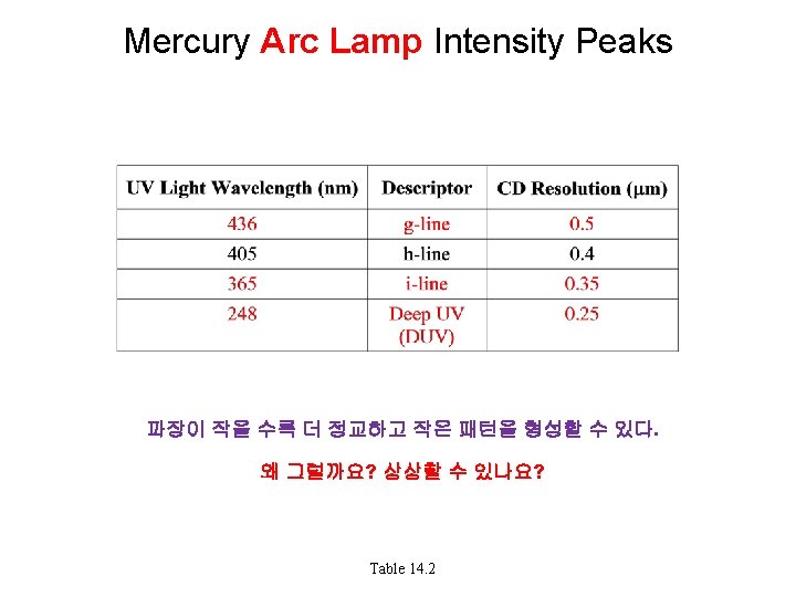
Emission Spectrum of Typical High Pressure Mercury Arc Lamp 필터를 통해 원하는 파장의 빛을 얻는다. 120 Emission spectrum of high-intensity mercury lamp i-line 365 nm Relative Intensity (%) 100 h-line 405 nm 80 g-line 436 nm 60 40 20 DUV 248 nm 0 200 300 400 500 600 Wavelength (nm) Mercury lamp spectrum used with permission from USHIO Specialty Lighting Products Figure 14. 7
Spectral Emission Intensity of 248 nm Excimer Laser vs. Mercury Lamp Kr. F laser 100 Excimer Laser가 선호 될까요? Mercury lamp가 선호될 까요? Relative Intensity (%) 80 60 40 20 Hg lamp 0 210 220 240 260 280 Wavelength (nm) 해당 파장의 intensity가 작다면 그만큼 많은 시간을 노출시켜야 한다. 이 경우에 생산량의 감소라는 불이익을 초래한다. Figure 14. 8
Excessive Resist Absorption of Incident Light Photoresist (after develop) Sloping profile Substrate 레지스트 바닥과 윗부분의 빛의 흡수 차이로 패턴이 경사를 가지게 된다. Figure 14. 9
Excimer Laser Sources for Semiconductor Photolithography 수은 lamp의 DUV 파장 intensity 약화로 새로운 광원의 필요성 대두됨 Table 14. 3
Spatial Coherence Incoherent light source of a single wavelength Black box illuminator Slit Two slits closely spaced Coherent cylindrical wave front Interference patterns Two coherent cylindrical wave fronts 빛의 간섭 현상으로 줄 무늬 패턴이 형성될 수 있는데, 광학적 기법으로 제 어되어야 한다. Figure 14. 10
Optical Lithography Optics • • • Reflection of Light(빛의 반사) Refraction of Light(빛의 굴절) Lens Diffraction(회절) Numerical Aperture, NA Antireflective Coating
Law of Reflection 빛의 입사각과 반사각은 같다 The angle of incidence of a light wavefront with a plane mirror is equal to the angle of reflection. Incident light i r Law of Reflection: i r Figure 14. 11 Reflected light
Application of Mirrors Illuminator for a simple aligner Flat mirror Ellipsoidal mirror Mask Flat mirror 거울을 따라 빛이 흘러가는 경로를 보세요 Used with permission from Canon USA Figure 14. 12
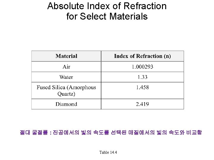
Refraction of Light Based on Two Mediums 빛의 굴절 • • fast medium glass (n 1. 5) Snell’s Law: sin i = n sin r Index of refraction, n = sin i / sin r slow medium air (n 1. 0) slow medium glass (n 1. 5) air (n 1. 0) fast medium 빛은 통과하는 매질의 경계면에서 매질에(매질의 굴절계수) 따라 굴절 된다. Figure 14. 13
Mirror Condenser lens Fly’s eye lens Collimator lens Flat mirror 많은 렌즈와 거울들로 구 성되어 있다. Illu m ina tor ass em bly Optical System of Lenses (렌즈를 이용한 광학 시스템) Masking unit Light sensor Optical filter Shutter Reticle stage (X, Y, ) Mercury lamp Lamp monitor Fiber optics Lamp position knob Ellipsoidal mirror X-drive motor Projection optics Optical focus sensor Interferometer mirror -Z drive stage 렌즈는 빛을 모아주는 역할 을 한다. Vacuum chuck Y-drive motor Wafer stage assembly Used with permission from Canon U. S. A. , FPA-2000 i 1 exposure system Figure 14. 14
Converging Lens with Focal Point (볼록 렌즈 : 한점에 집중) 2 f f = focal length F = focal point S = 2 f O = origin, center of lens f S Object F O Figure 14. 15 F´ Real image S´
Diverging Lens with Focal Point (오목 렌즈 : 분기) f = focal length F = focal point S = 2 f O = origin, center of lens S Object Virtual image F O Figure 14. 16 F´ S´
Laser-Induced Lens Compaction Compacted area of lens Figure 14. 17
Interference Pattern from Light Diffraction at Small Opening (회절 패턴) • • • Light travels in straight lines. Diffraction occurs when light hits edges of objects. Diffraction bands, or interference patterns, occur when light waves pass through narrow slits. Diffraction bands Figure 14. 18
Diffraction in a Reticle Pattern Diffracted light rays Slit Plane light wave 회절에 의해 일어난 간섭 패턴은 작은 접촉 홀과 라인을 패턴 화 하는 것을 어렵게 만든다. Figure 14. 19
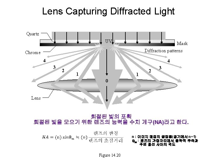
Effect of Numerical Aperture on Imaging Pinhole masks Lens NA 小 Image results Bad Expos ure lig ht Poor Good Diffracted light 大 렌즈의 크기를 크게 함으로써 양호한 패턴을 얻을 수 있으나 그 만큼 고가의 큰 렌즈를 제작해야 하고, 시스템이 복잡해 진다. Figure 14. 21
Typical NA Values for Photolithography Tools Table 14. 5
Photoresist Reflective Notching Due to Light Reflections UV exposure light Mask Edge diffraction Surface reflection Unexposed photoresist Exposed photoresist Polysilicon Notched photoresist STI Substrate 빛의 반사에 의해 원하지 않는 PR 지역에 빛이 들어가 PR을 변 형시켜 패턴에 흠이 생기는 것을 노칭(notiching)이라고 한다. Figure 14. 22
Incident and Reflected Light Wave Interference in Photoresist Standing wave effect Incident wave Reflected wave Photoresist Film Substrate Standing waves cause nonuniform exposure along the thickness of the photoresist film. Figure 14. 23
Effect of Standing Waves in Photoresist Standing wave 효과에 의해 생긴 패턴 Photo 14. 1
Antireflective Coating to Prevent Standing Waves Incident wave Photoresist Antireflective coating Film Substrate The use of antireflective coatings, dyes, and filters can help prevent interference. Standing wave 효과를 줄이기 위해 ARC(antireflective coating) 층 을 증착하여 반사파를 줄인다. Figure 14. 24
Light Suppression with Bottom Antireflective Coating UV exposure light Mask Unexposed photoresist Exposed photoresist Polysilicon BARC STI Substrate Standing wave 효과를 줄이기 위해 ARC(antireflective coating) 층 을 증착하여 반사파를 줄인다. Figure 14. 25
BARC Phase-Shift Cancellation of Light (A) Incident light Photoresist (B) Top surface reflection (C) (D) C and D cancel due to phase difference BARC (Ti. N) Aluminum Figure 14. 26
Top Antireflective Coating Incident light Resist-substrate reflections Incident light Top antireflective coating absorbs substrate reflections. Photoresist Substrate reflection Substrate Figure 14. 27
Optical Lithography Resolution • Calculating Resolution • Depth of Focus • Resolution Versus Depth of Focus – Surface Planarity
Resolution of Features (분해능) The dimensions of linewidths and spaces must be equal. As feature sizes decrease, it is more difficult to separate features from each other. 패턴을 큰 사이즈에서 작은 사이즈까지 마스크에 그려 놓고 이 를 평가하여 Resolution을 평가한다. Figure 14. 28
Calculating Resolution for a given , NA and k (매우 중요) R= k = 0. 6 K: 공정 요소, 0. 6~0. 8 : 공정 nohow! λ: 광원의 파장 NA : 렌즈의 구경 Illuminator, Mask i-line Lens, NA DUV Wafer k NA 365 nm 193 nm 0. 45 0. 60 R 486 nm 365 nm 257 nm 193 nm R 분해능은 파장이 짧을수록, NA(개구)가 클수록 값이 작아지고 따 라서 미세패턴을 형성 할 수 있다. Figure 14. 29
Depth of Focus (DOF) (매우 중요) Lens Center of focus Depth of focus Photoresist + Film 초점의 범위, 영상 전체의 연속적인 초점을 초점의 깊이라고 한다. Center of focus(COF)는 가장 우수한 이미지를 얻을 수 있는 곳 Figure 14. 30
Resolution Versus Depth of Focus for Varying NA (매우 중요함) DOF = Illuminator, i-line Mask DUV 2(NA)2 R DOF 365 nm 193 nm 0. 45 0. 60 486 nm 365 nm 257 nm 193 nm 901 nm 507 nm 476 nm 268 nm Lens, NA Center of focus - Depth of focus Photoresist Wafer DOF + DOF가 작아지면 PR 두께는 어찌 해야 하는가? Figure 14. 31 Film
Photolithograhy Equipment (장비의 발전 역사) • • • Contact Aligner Proximity Aligner Scanning Projection Aligner (scanner) Step-and-Repeat Aligner (stepper) Step-and-Scan System
Contact/Proximity Aligner System Contact align 장비는 mask와 wafer가 접 촉한다. 어떤 문제가 있을 수 있을까? Mercury arc lamp Illuminator Alignment scope (split vision) Mask stage (X, Y , Z , q) Wafer stage (X, Y, Z, q) Mask와 Wafer를 왜 움직여야 하나? Vacuum chuck Used with permission from Canon USA, Figure 14. 32
Edge Diffraction and Surface Reflectivity on Proximity Aligner Mask와 Wafer 사이가 2. 5μm에서 25 μm 정도 떨어져 있다. UV exposure light Mask UV Diffracted and reflected light Resist Substrate Gap Substrate Diffraction of light on edges results in reflections from underside of mask causing undesirable resist exposure. Figure 14. 33
Scanning Projection Aligner Mercury arc lamp Wafer Illuminator assembly Mask의 국부적인 부분을 빛을 쬐고 이것을 scanning 하여 wafer의 전면에 쬐어 준다. Mask Scan direction p je Pro ct o n o i tics b m e s ly as Exposure light (narrow slit of UV gradually scans entire mask field onto wafer) Redrawn and used with permission from Silicon Valley Group Lithography Figure 14. 34
Step-and-Repeat Aligner (Stepper) Used with permission from Canon USA, FPA-3000 i 5 (original drawing by FG 2, Austin, TX) Figure 14. 35
Stepper Exposure Field Mask의 국부적인 부분을 빛을 쬐고 이것을 scannin 하여 wafer의 전 면에 쬐어 준다. UV light Reticle field size 20 mm × 15 mm, 4 die per field 5: 1 reduction lens Image exposure on wafer 1/5 of reticle field 4 mm × 3 mm, 4 die per exposure Serpentine stepping pattern Wafer Figure 14. 36
Wafer Exposure Field for Step-and-Scan Stepper Image Field (single exposure) Step and Scan Image Field 둘 사이의 차이점은? Reticle UV Reticle Scan UV 5: 1 lens 4: 1 lens Wafer Stepping direction Scan Redrawn and used with permission from ASM Lithography Figure 14. 37
Step and Scan Exposure System Illuminator optics Reticle library (SMIF pod interface) Excimer laser (193 nm Ar. F ) Beam line Wafer transport system Operator console Reticle stage Wafer stage Auto-alignment system 4: 1 Reduction lens NA = 0. 45 to � 0. 6 Used with permission from ASML, PAS 5500/900 Figure 14. 38
Reticles • • • Comparison of Reticle Versus Mask Reticle Materials Reticle Reduction and Size Reticle Fabrication Sources of Reticle Damage
Comparison of Reticle Versus Mask 표 14 -6 page 482 읽어 보세요 Table 14. 6
Photolithography Reticle Photograph courtesy of Advanced Micro Devices Photo 14. 2
Comparison of Reticle Reduction Versus Exposure Field size on reticle Projection lens Exposure field on wafer Figure 14. 39
Principles of Electron Beam Lithography Work Station Electronics Console Vacuum control module Printer/Plotter TFE electron source control Electron beam control Servo control Stage position control 9 -track magnetic tape drive Control Height deflection computer and Operator Super dynamic console flash correction HTM Height detection assembly Data direct computer Transfer and drive TFE electron beam column Automatic loading chamber Work stage Work table Work chamber, load chamber, vibration isolation, ion pump, and vacuum system Reticle을 만드는 데 Utility Console 오랜 기간이 필요하 Temperature Air and Cassette control nitrogen clamping 다. control Water chiller Coolant flow control Roughing pump Backing pump Used with permission from Etec Systems, Inc. , MEBES 4500 Systems Figure 14. 40 Beam control and deflection Dynamic corrections
Pellicle on a Reticle Pellicle film Chrome pattern Frame Reticle The particle on the pellicle surface is outside of optical focal range. Antireflective coatings Pellicle film Chrome pattern Depth of focus Mask material Figure 14. 41
Optical Enhancement Techniques (광학 개선 기술) • • Phase-Shift Mask (PSM) Optical Proximity Correction (OPC) Off-Axis Illumination Bias
Phase-Shifting Mask 레티컬에서 발생되는 회절 문제를 해 결하기 위해 사용함 a) BIM Chrome b) APSM Absortive phase shifters c) Rim PSM Rim phase shifters Electric +1 field on 0 mask -1 Electric field on wafer +1 0 -1 Intensity on +1 wafer 0 Reprinted from the January 1992 edition of Solid State Technology, copyright 1992 by Penn. Well Publishing Company Figure 14. 42 Blockers
Off-Axis Illumination Conventional illumination (on-axis) A Off-axis illumination B Pinhole mask A+ B- Order diffraction + Order diffraction B+ A- Projection optics Wafer (a) (b) Figure 14. 44
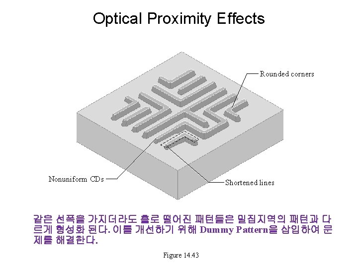
Serifs to Minimize Rounding of Contact Corners (a) Uncorrected design (b) Corrected with feature biasing (c) Feature assisting technique Bias : 웨이퍼상에 원래 만들고자 하는 패턴의 사이즈와 실제 사이즈 사이의 차이를 지칭한다. 그림과 같이 corner의 pattern을 변형 시켜 원래 사이드를 만든다. 이 때 추가 붙여준 패턴을 세리프(serifs)라고 한다. Figure 14. 45
Alignment • • Baseline Compensation Overlay Accuracy Alignment Marks Types of Alignment
Overlay Budget 두개의 패턴사이에 정렬되어 있는 가를 판단한다. -DY Shift in registration Perfect overlay accuracy +Y +Y -X -Y Reticle pattern -X +X DX Wafer pattern Figure 14. 46 +X -Y
Grid of Exposure Fields on Wafer Stop 32 31 30 29 23 24 25 26 27 28 22 21 20 19 18 17 11 12 13 14 15 16 10 9 8 7 6 5 2 3 4 Start 1 Figure 14. 47
Step-and-Repeat Alignment System Used with permission from Canon USA, FPA-2000 i 1 Figure 14. 48
Alignment Marks + GA + FAR RAR + RA, Reticle alignment marks, L/R GA, Wafer global alignment marks, L/R + FA, Wafer fine alignment marks, L/R + + GAR FAL/R + + FAL + RAL 1 st Mask + GAL FAR For 2 nd mask 1 st mask layer { FAL/R + + + From 1 st mask FAL 2 nd Mask 2 nd mask layer Figure 14. 49 Notch, coarse alignment
On-Axis Versus Off-Axis Alignment System On-Axis Alignment System Microscope objectives for video camera Reticle Alignment laser (633 nm) Alignment BLC fiducial Projection optics Off-axis alignment unit Alignment BLC fiducial Wafer stage Used with permission from Canon USA, redrawn after FPA-2000 i 1 schematics Figure 14. 50 Video Optical fiber Alignment laser (633 nm)
Environmental Conditions (매우 중요) • • • Temperature Humidity Vibration Atmospheric Pressure Particle Contamination Page 493~494 읽어 보세요
Comparison of Photo Tools (Refer to Table 14. 7) • • Models by Manufacturer Wavelength (nm) Type of Aligner Illumination Type Exposure Field Size (mm) Resolution (mm) Overlay Accuracy (nm) 표 14 -7 : 표를 보고 느낌점을 말해 보세요… 무엇을 써놓은 건가요?
Step-and-Scan Aligner Photograph courtesy of Silicon Valley Group Lithography, Micrascan II Photo 14. 3
Chapter 14 Review • • Quality Measures Troubleshooting Summary Key Terms Review Questions Equipment Suppliers’ Web Sites References 407 408 409 410 411 412