Semiconductor Manufacturing Technology Chapter 11 Deposition Objectives After

Semiconductor Manufacturing Technology Chapter 11 Deposition 증착

Objectives After studying the material in this chapter, you will be able to: 1. Describe multilayer metallization. Discuss the acceptable characteristics of a thin film. State and explain the three stages of film growth. 2. Provide an overview of the different film deposition techniques. 3. List and discuss the 8 basic steps to a chemical vapor deposition (CVD) reaction, including the different types of chemical reactions. 4. Describe how CVD reactions are limited, reaction dynamics and the effect of dopant addition to CVD films. 5. Describe the different types of CVD deposition systems, how the equipment functions and the benefits/limitations of a particular tool for film applications. 6. Explain the importance of dielectric materials for chip technology, with applications. 7. Discuss epitaxy and three different epi-layer deposition methods 8. Explain spin on dielectrics.

Film Layers for an MSI Era NMOS Transistor Nitride Topside Oxide Metal Pad Poly n+ Pre-metal oxide Sidewall oxide Gate oxide ILD Oxide Field oxide n+ Poly p+ n-well p- epi layer p+ silicon substrate Figure 11. 1 Metal p+

Process Flow in a Wafer Fab Locations where thin films are deposited Wafer fabrication (front-end) Wafer start Thin Films Polish Photo Etch Unpatterned wafer Completed wafer Diffusion Test/Sort Implant 얇은 막을 wafer에 입히는 공정이 증착(Deposition) 공정이다. Figure 11. 2

Introduction • Film Layering in Wafer Fab – Diffusion – Thin Films • Film Layering Terminology • Multilayer Metallization – Metal Layers – Dielectric Layers

Multilevel Metallization on a ULSI Wafer Passivation layer Bonding pad metal ILD-6 ILD-5 M-4 금속층 : 도체 Polysilicon, L 1 metal M 1~M 4, Pad Metal ILD-4 M-3 ILD-3 M-2 유전체층 : 절연체 STI Oxide, L 1 Oxide ILD-1~ILD-6, Passivation Layer ILD-2 M-1 Via ILD-1 Poly gate LI metal 그림에서 어떤 규칙성이? n+ p+ LI oxide p+ STI n-well n+ p-well p- Epitaxial layer p+ Silicon substrate Figure 11. 3 n+ p+

Metal Layers in a Chip Passiv ation ILD-6 layer M-4 Bonding pad metal ILD-5 ILD-4 M-3 ILD-3 M-2 ILD-2 M-1 V ILD-1 i a. Poly gate. LI oxide LI metal n+ p+ p+ STI n+ n-well p- Epitaxial layer p+ Silicon substrate 절연층(Oxide)을 제거하고 금속층만 보이게 만든것……. 어떤 그림이 떠오르는가요? 비유적으로… Photo 11. 1 n+ p+
 · Good step coverage · Ability to")
Film Deposition Thin Film Characteristics (매우 중요) · Good step coverage · Ability to fill high aspect ratio gaps (conformality) · Good thickness uniformity · High purity and density · Controlled stoichiometries · High degree of structural perfection with low film stress · Good electrical properties · Excellent adhesion to the substrate material and subsequent films

Solid Thin Film Thickness Le n gt h Width Thin films are very thin in comparison to the substrate. Oxide Silicon substrate Figure 11. 4

1. Film Coverage over Steps Uniform thickness Conformal step coverage Nonconformal step coverage 왜 왼쪽 그림이 더 바람직한 모습인가요? Figure 11. 5

2. Aspect Ratio for Film Deposition Aspect Ratio = Depth Aspect Ratio = Width D 500 Å 250 Å 500 Å W 왜 HIGH Aspect Ratio가 요구 될까요? Figure 11. 6 250 Å = 2 1

High Aspect Ratio Gap Photograph courtesy of Integrated Circuit Engineering Photo 11. 2
 막 성장 Model Gas molecules Coalescence 융합, 유체 Nucleation")
Stages of Film Growth(매우 중요) 막 성장 Model Gas molecules Coalescence 융합, 유체 Nucleation 핵형성 Substrate 비정질이나 다결정 형태로 형성된다. Figure 11. 7 Continuous film 연속적인 성장
 화학과 물리는 어떤 의미가 있나? Table 11. 1")
Techniques of Film Deposition(매우 중요) 화학과 물리는 어떤 의미가 있나? Table 11. 1

Chemical Vapor Deposition The Essential Aspects of CVD 1. Chemical action is involved, either through chemical reaction or by thermal decomposition (referred to as pyrolysis(열분해). 2. All material for the thin film is supplied by an external source. 3. The reactants in a CVD process must start out in the vapor phase (as a gas).

Chemical Vapor Deposition Tool Photograph courtesy of Novellus, Sequel CVD Photo 11. 3
 with the")
CVD Chemical Processes 1. Pyrolosis: a compound dissociates (breaks bonds, or decomposes) with the application of heat, usually without oxygen. 2. Photolysis: a compound dissociates with the application of radiant energy that breaks bonds. 3. Reduction: a chemical reaction occurs by reacting a molecule with hydrogen. 4. Oxidation: a chemical reaction of an atom or molecule with oxygen. 5. Reduction-oxidation (redox): a combination of reactions 3 and 4 with the formation of two new compounds. CVD 공정의 기본적인 화학반응들…

CVD Reaction • • • CVD Reaction Steps Rate Limiting Step CVD Gas Flow Dynamics Pressure in CVD Doping During CVD – PSG – BSG – FSG
 1) Mass transport of reactants CVD Reactor 1. 증착존으로Gas delivery")
CVD Reaction Steps(매우 중요) 1) Mass transport of reactants CVD Reactor 1. 증착존으로Gas delivery 가스 이동 8) By 7) Desorption of product byproducts 2. 박막 전구체 2) Film removal Byprecursor Exhaust 의 형성 reactions products 3. 웨이퍼에서의 3) Diffusion of gas Continuous 5) Precursor 박막 전구체 molecules 6) Surface film diffusion into reactions 4) Adsorption substrate 4. 전구체 흡착 of precursors 5. 전구체 확산 Substrate 6. 표면 반응 Schematic of CVD Transport and Reaction Steps 7. 표면에서의 부산물 제거 (1) Si. H 4 Si. H 2+H 2 (2) Si. H 4+Si. H 2 Si 2 H 6 (3) Si 2 H 6 2 Si+3 H 2 8. 반응기에서

Rate Limiting Step 표면에서의 반응률은 온도 증가 와 함께 증가한다. CVD 반응은 순차적이기 때문에 가장 1) Mass transport of늦은 단계가 전체 공정에서 CVD Reactor reactants Gas delivery 병목 현상을 만든다. 2) Film precursor reactions 3) Diffusion of gas molecules 4) Adsorption of precursors 7) Desorption of byproducts By-products 5) Precursor diffusion into substrate 8) By-product removal Exhaust 6) Surface reactions Substrate Continuous film

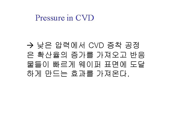
CVD Gas Flow Dynamics 기체 흐름 역학은 균일한 막 증 착을 위해 매우 중요하다. 기체 상태에서 웨이퍼 표면까지 의 기체 운반은Gas확산(Diffusion)의 flow 메커니즘이다. Diffusion of reactants Reaction product Deposited film Silicon substrate

Gas Flow Dynamics at the Wafer Surface Gas flow Boundary layer Stagnant layer Figure 11. 10

Doping during CVD • CVD 증착 공정에서 불순물을 삽입하 여 Doping을 진행 할 수 있다. Si. H 4(gas) + 2 PH 3(gas) + O 2(gas) Si. O 2(solid) + 2 P(solid) + 5 H 2(gas) silane phosphine oxygen silicon dioxide phosphorus hydrogen • 막의 집적도 개선이나 응력을 감소시 키기 위해 불순물을 넣어 주는 경우 도 있다. • Borosilicate Glass : BSG • Borophosilicate Glass : BPSG
 • CVD Equipment Design – CVD reactor heating – CVD")
CVD Deposition Systems(빨간색 중요함) • CVD Equipment Design – CVD reactor heating – CVD reactor configuration – CVD reactor summary • • • Atmospheric Pressure CVD, APCVD Low Pressure CVD, LPCVD Plasma-Assisted CVD Plasma-Enhanced CVD, PECVD High-Density Plasma CVD, HDPCVD

CVD Reactor Types 압력으로 구분 Figure 11. 11 공정 진행 wafer 장수
 책 page 332 표 11 -2")
Types of CVD Reactors and Principal Characteristics(매우 중요함) 책 page 332 표 11 -2 읽어 보기 Table 11. 2

Continuous-Processing APCVD Reactors Reactant gas 1 2가지 종류의 APCVD System Inert separator gas Film Reactant gas 2 Wafer (a) Gas-injection type PSG, BPSG, FSG 증착에 사용 N 2 Reactant gases N 2 N 2 Wafer Heater (b) Plenum type Figure 11. 12
수")
Excellent Step Coverage of APCVD TEOS-O 3 매우 높은 Aspect ratio에서도 hole을 매울 (gap-fill)수 있는 능 력이 있다 Figure 11. 3

Planarized Surface after Reflow of PSG 왼쪽 그림과 오른쪽 그림의 차이점은? Before reflow After reflow PSG Metal or polysilicon Figure 11. 14

Boundary Layer at Wafer Surface LPCVD Continuous gas flow Diffusion of reactants Boundary layer Deposited film Silicon substrate ü 낮은 가격, 높은 생산 처리량, 우수한 막 특성으로 가장 많이 사용된다. ü 진공은 0. 1~5 torr, 온도는 200 o. C~900 o. C ü 반응로는 수직 또는 수평으로 구성되어 있음 Figure 11. 15

LPCVD Reaction Chamber for Deposition of Oxides, Nitrides, or Polysilicon Three-zone heating element Pressure gauge Exhaust to vacuum pump Gas inlet Profile thermocouples (internal) Spike thermocouples (external, control) ü 구조가 매우 간단해 보이지 않나요? Figure 11. 16

Oxide Deposition with TEOS LPCVD Computer terminal operator interface TEOS, Si. O 2, Si 3 N 4, Polysilicon 박막 증착에 사용 Gas flow controller Furnace microcontroller LPCVD Furnace N 2 Temp. controller Threezone heater O 2 Heater TEOS ü 앞 그림과 무엇이 다른가요? Figure 11. 17 Pressure controller Exhaust Vacuum pump

Key Reasons for the Use of Doped Polysilicon in the Gate Structure Page 338 좌측 하단의 책 부분 읽어 보세요! 1. Ability to be doped to a specific resistivity. 2. Excellent interface characteristics with silicon dioxide. 3. Compatibility with subsequent high temperature processing. 4. Higher reliability than possible metal electrodes (e. g. , aluminum) 5. Ability to be deposited conformally over steep topography. 6. Allows for self-aligned gate process (see Chapter 12).

Doped Polysilicon as a Gate electrode n+ p+ p+ n+ Figure 11. 18 n+ p+
. 2. Excellent")
Advantages of Plasma Assisted CVD 1. Lower processing temperature (250 – 450°C). 2. Excellent gap-fill for high aspect ratio gaps (with highdensity plasma). 3. Good film adhesion to the wafer. 4. High deposition rates. 5. High film density due to low pinholes and voids. 6. Low film stress due to lower processing temperature. Page 340 우측 상단의 책 부분 읽어 보세요!

Film Formation during Plasma-Based CVD Gas 분해를 위한 에너지로 Plasma를 사용한다 RF generator Electrode 1) Reactants enter chamber Gas delivery 7) Desorption of by-products 2) Dissociation of reactants by electric fields 3) Film precursors are formed 4) Adsorption of precursors PECVD reactor RF field By-products 8) By-product removal Exhaust 5) Precursor diffusion 6) Surface reactions into substrate Continuous film Substrate Electrode Gas 분해를 위해 Plasma를 사 용하는 것을 제외하고 반응의 주요 공정은 비슷함 Figure 11. 19 Plasma에 대해 조사하여 PPT 형 식으로 보고서를 작성하여 제출한 다.

General Schematic of PECVD for Deposition of Oxides, Nitrides, Silicon Oxynitride or Tungsten Matching network Gas dispersion screen RF generator Microcontroller operator Interface Gas flow controller Pressure controller Gas panel Electrodes Turbo pump 공정 반응실을 제외하고 나머 지는 비슷하죠. Process gases PECVD 공정은 LPCVD 공정 온도에 비해 낮다. Figure 11. 20 Exhaust Roughing pump

Properties of Silicon Nitride for LPCVD Versus PECVD Table 11. 3

High Density Plasma Deposition Chamber • Popular in mid-1990 s • High density plasma • Highly directional due to wafer bias • Fills high aspect ratio gaps • Backside He cooling to relieve high thermal load • Simultaneously deposits and etches film to prevent bread-loaf(덩어리) and key-hole effects Photograph courtesy of Applied Materials, Ultima HDPCVD Centura Photo 11. 4

Dep-Etch-Dep Process Bread-loaf effect Si. O 2 The solution begins here Key-hole defect Metal Film deposited with PECVD creates pinch-off at the entrance to a gap resulting in a void in the gap fill. 1) Ion-induced deposition of film precursors Cap 2) Argon ions sputter-etch excess film at gap entrance resulting in a beveled appearance in the film. 3) Etched material is redeposited. The process is repeated resulting in an equal “bottom-up” profile. Figure 11. 21

Five Steps of HDPCVD Process 1. Ion-induced deposition 2. Sputter etch 3. Redeposition 4. Hot neutral CVD 5. Reflection

HDPCVD with Wafer at Throat of Turbo Pump Microwave 2. 45 GHz Electromagnet Gas shower head Wafer on electrostatic chuck Gate valve Turbo pump To roughing pump Figure 11. 22
 HDPCVD")
3 -Part Process for Dielectric Gap Fill Si. O 2 Cap Aluminum 1) HDPCVD gap fill 2) PECVD cap Figure 11. 23 3) Chemical mechanical planarization
 Gap Fill Chip Performance Low-k")
Dielectrics and Performance • • • Dielectric Constant(유전 상수) Gap Fill Chip Performance Low-k Dielectric High-k Dielectric Device Isolation – LOCOS – STI
 vs. Feature Size ( m) 2. 5 Interconnect delay (RC) Delay")
Interconnect Delay (RC) vs. Feature Size ( m) 2. 5 Interconnect delay (RC) Delay time (´ 10 -9 sec) 2. 0 1. 5 Gate delay 1. 0 0. 5 0 0 . 5 1. 0 1. 5 2. 0 Feature size ( m) C 값이 증가할 수록 RC 값은 커지고 속도가 저하된다. 따라서 낮은 유전상수를 갖는 물질이 필요하다. Figure 11. 24
 6 5 4 K=4 3")
Total Interconnect Wiring Capacitance 7 Capacitance (10 -12 Farads/cm) 6 5 4 K=4 3 K=3 2 K=2 1 K= 1 0 0 0. 5 1. 0 1. 5 2. 0 2. 5 3. 0 Space ( m) Redrawn with permission from Semiconductor International, September 1998 Figure 11. 25

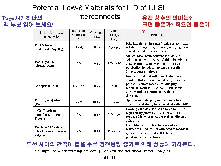
Low-k Dielectric Film Requirements 중요함 Page 350 상단의 표 11 -5 읽어 보세요! Table 11. 5
 Doped polysilicon capacitor plate(도체)")
General Diagram of DRAM Stacked Capacitors Si. O 2 dielectric(절연체) Doped polysilicon capacitor plate(도체) Buried contact diffusion DRAM에서 절연체로 사용되는 산화막은 높은 k를 요구한다. 왜냐하면 높은 정전용량이 필요하기 때문이다. 또한 MOSFET의 gate 물질도 높은 유전상수 k가 요구되어 진다. (Why? ) Figure 11. 26

Shallow Trench Isolation 예전의 LOCOS 방식의 소자 분리 기술이 최근에는 많은 장점을 제공해 주는 상기와 같은 Shallow Trench Isolation (STI) 기술로 발전하였다. Photograph courtesy of Integrated Circuit Engineering Photo 11. 5
 • Spin-on Dielectric (SOD) • Epitaxy – Epitaxy")
Spin-on Dielectrics • Spin-on Glass (SOG) • Spin-on Dielectric (SOD) • Epitaxy – Epitaxy growth methods • Vapor-phase epitaxy • Metalorganic CVD • Molecular-beam epitaxy • Quality Measures • CVD Troubleshooting
 경화과정을 거쳐 Si. O 2처럼 단단한 물질로 바뀐다. 줄 틈")
Gap-Fill with Spin-On-Glass (SOG) 경화과정을 거쳐 Si. O 2처럼 단단한 물질로 바뀐다. 줄 틈 채우기 공정에 사용된다. Cap 1) Initial SOG gap fill 2) SOG after curing Figure 11. 27 3) CVD oxide cap

Proposed HSQ Low-k Dielectric Processing Parameters 낮은 유전상수 값을 요구 할 때 사용된다 Table 11. 6
 –")
Epitaxy • Epitaxy Growth Model • Epitaxy Growth Methods – Vapor-Phase Epitaxy (VPE) – Metalorganic CVD (MOCVD) – Molecular-Beam Epitaxy (MBE)

Silicon Epitaxial Growth on a Silicon Wafer 단일 결정체의 기판 표면 위에 단일 결정 물질을 성장 시키는 것 성장 시키기 전에 Si 표면을 매우 청결하게 하는 것이 중요하다. Si H H H Cl Cl Cl By-products Cl Chemical reaction Deposited silicon H Si Si Epitaxial layer Si Si Single silicon substrate Figure 11. 28

Illustration of Vapor Phase Epitaxy RF induction-heating coils Vacuum puimp Wafers H 2 Si. H 2 Cl 2 Dopant (As. H 3 or B 2 H 3) Susceptor Figure 11. 29

Silicon Vapor Phase Epitaxy Reactors Gas inlet RF heating Exhaust Horizontal reactor Vertical reactor Figure 11. 30 Exhaust Barrel reactor

Effects of Keyholes in ILD on Metal Step Coverage Keyhole defect in interlayer dielectric Aluminum Si. O 2 a) Si. O 2 deposited by PECVD b) Si. O 2 is planarized Metal void caused by keyhole defect in Si. O 2 c) Next layer of aluminum is deposited Figure 11. 31

Chapter 11 Review • • Deposition Quality Measures 292 Troubleshooting Summary 292 294 Key Terms Review Questions 295 Equipment Suppliers’ Web Sites References 296
- Slides: 61