Semiconductor laser structure n n n PN junction


![Semiconductor optical amplifier • ( )=N 0 [ 2/(8 tsp)] g( ) Gain coefficient](https://slidetodoc.com/presentation_image_h2/7f0f98b837c4c114697b10d4f6629d8d/image-12.jpg "Semiconductor optical amplifier • ( )=N 0 [ 2/(8 tsp)] g( ) Gain coefficient")


 • Central wavelength • FWHM • Mode spacing 1580 1575")
 =q /2 n n n 在active layer邊長 出corrugated waveguide. 在兩端作AR")


- Slides: 23
Semiconductor laser structure n n n P-N junction laser Heterojuction laser DH laser
Laser mode Strip laser Mode confined laser
Far field pattern n n Laser diode is mounted on a rotating stage. The angular dependence is recorded. detector preamplifier Amplifier/averager
L-I curve • I< Ith spontaneous emission • Wide linewidth • Similar to LED • I= Ith gain>loss start lasing • Mode distribution change • I> Ith stimulated emission • Narrow linewidth • Modulation range
L-I curve n n n Temperature, then Ith . Temperature , then slope efficiency . Kink---mode hopping P (m. W) 25℃ 45℃ 70℃ I (m. A)
Semiconductor optical amplifier • ( )=N 0 [ 2/(8 tsp)] g( ) Gain coefficient 高低能階 粒子數差 Lineshape function • Lineshape function: • Solve S. E. • Gain coefficient: 為半 導體材質造成的增益 ! Gain coefficient Amplifier gain o
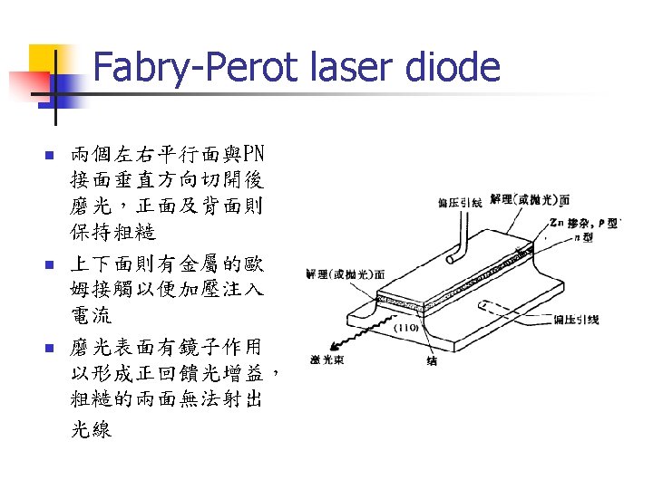
Fabry-Perot laser diode—optical oscillator cavity n n Fabry-Perot resonator--parallel front and rear surface. Cleaving the crystal along LD crystalline planes. R~33%(n. In. Ga. As. P=3. 71) Mode spacing=c/2 L HR layer Active region Cavity length height width Height: 0. 1~0. 2 mm Length: 250~500 mm Width: 5~15 mm Sides: rough cut Front: cleaved HR layer: ~90%
FP LD---spectral distribution Gain coefficient Amplifier gain Gain profile c/2 L o Resonance cavity modes o Lasing modes
FP LD---spectral distribution wavelength(nm) • Central wavelength • FWHM • Mode spacing 1580 1575 1570 1565 1560 1555 1550 1545 Wavelength(nm) 1568 1566 1564 1562 1560 1558 1556 1554 1552 1550 A 3 A 5 C 1 C 3 C 5 D 4 0 20 40 60 80 current(m. A) 100 120 A 3 A 5 C 1 C 3 C 5 D 4 14 16 18 20 22 24 26 28 30 32 Temperature(℃)
Distributed feedback laser(DFB laser) =q /2 n n n 在active layer邊長 出corrugated waveguide. 在兩端作AR coating, 減少平面反射。 Spectral linewidth~10 MHz =q /2 SMSR Guiding layer Active layer p p p n
Quantum well laser n n n Double hetero-junction structure consisting of an ultra thin layer(<=50 nm) of semiconductor material. Quantum well n Layer thickness <de broglie (50 nm) energy state quantized density of states quantized Electrons accumulate in conduction band well, and holes in valence band well. E z bulk d 1 Eg 1 x Eg 2 x Density of states
Quantum well laser n Gain of QW laser n n Advantages n n n Better performance than bulk laser low threshold current Narrower spectrum of gain coefficient Smaller linewidth Higher modulation frequency Reduced temperature dependence MQW laser is superior than SQW laser at high current density. Peak gain coefficient QW laser 2 m Bulk DH m JT 1 JT 2 Current density J
Semiconductor laser package
Gain guided and index guided laser
Laser diode modulation
Tracking error
Relative intensity noise