Semiconductor Devices Prof Zbigniew Lisik Department of Semiconductor
Semiconductor Devices Prof. Zbigniew Lisik Department of Semiconductor and Optoelectronics Devices room: 116 e-mail: zbigniew. lisik@p. lodz. pl Chapter 2 Phenomena in Semiconductors IFE T&CS
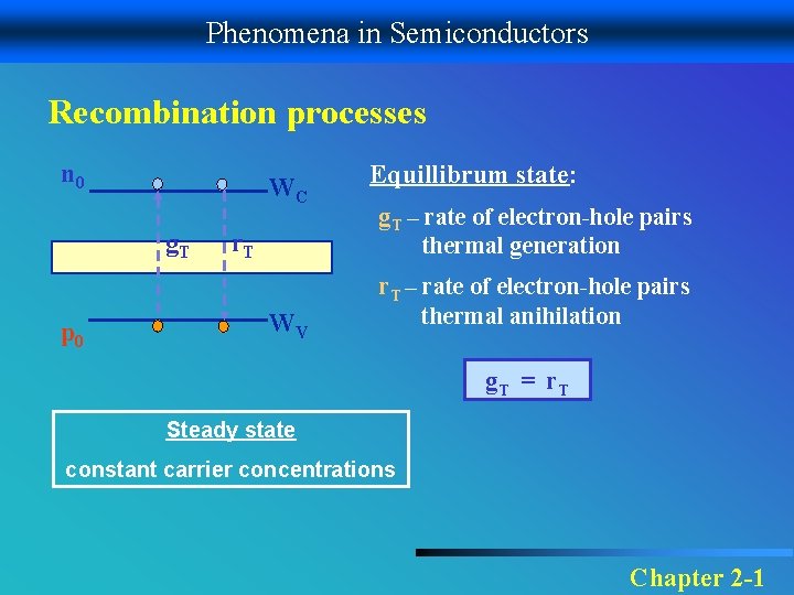
Phenomena in Semiconductors Recombination processes n 0 WC g. T p 0 r. T WV Equillibrum state: g. T – rate of electron-hole pairs thermal generation r. T – rate of electron-hole pairs thermal anihilation g. T = r. T Steady state constant carrier concentrations Chapter 2 -1
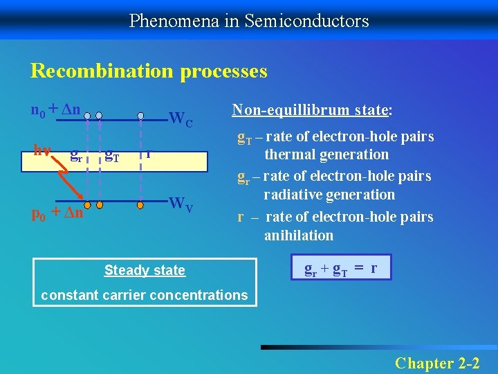
Phenomena in Semiconductors Recombination processes n 0 + Δn h gr p 0 + Δn WC g. T r WV Non-equillibrum state: g. T – rate of electron-hole pairs thermal generation gr – rate of electron-hole pairs radiative generation r – rate of electron-hole pairs anihilation Steady state gr + g. T = r constant carrier concentrations Chapter 2 -2

Phenomena in Semiconductors Recombination processes n 0 + Δn WC g. T p 0 + Δn Non-equillibrum state: r WV g. T – rate of electron-hole pairs thermal generation r – rate of electron-hole pairs anihilation Transient state g. T < r vary carrier concentrations R = r - g. T R – recombination rate Chapter 2 -3

Phenomena in Semiconductors Recombination processes n = n 0 + n - lifetime n 0 n n = n 0 exp (-t/ ) n(3 ) = 0. 05 n 0 t Chapter 2 -4

Phenomena in Semiconductors Recombination processes Phonon Recombination – the whole energy Wg is taken by thermal vibration of atoms in the lattice, called phonons (Rph , ph) Auger (impact) Recombination – the whole energy Wg is taken be third carrier, electron or hole, called the hot carrier (RA , A) Radiative Recombination – the whole energy Wg is taken be a new created photon that can leave the crystal e. g. as the visible radiation (Rr , r) R = Rph + RA + Rr Chapter 2 -5
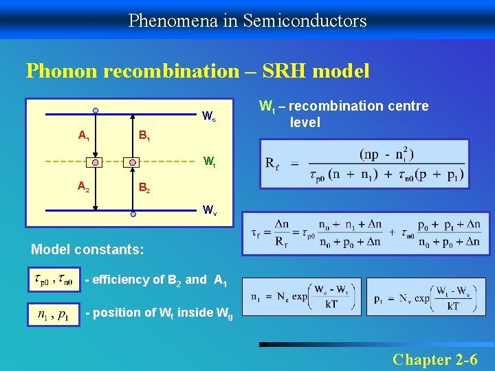
Phenomena in Semiconductors Phonon recombination – SRH model Wc A 1 B 1 Wt – recombination centre level Wt A 2 B 2 Wv Model constants: - efficiency of B 2 and A 1 - position of Wt inside Wg Chapter 2 -6
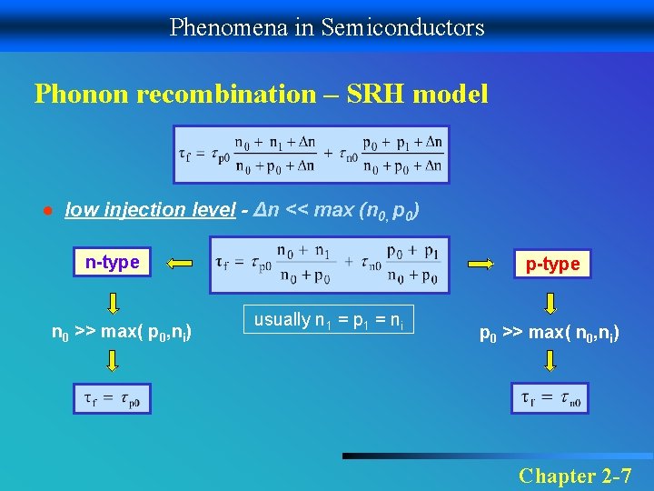
Phenomena in Semiconductors Phonon recombination – SRH model ● low injection level - Δn << max (n 0, p 0) n-type n 0 >> max( p 0, ni) p-type usually n 1 = p 1 = ni p 0 >> max( n 0, ni) Chapter 2 -7
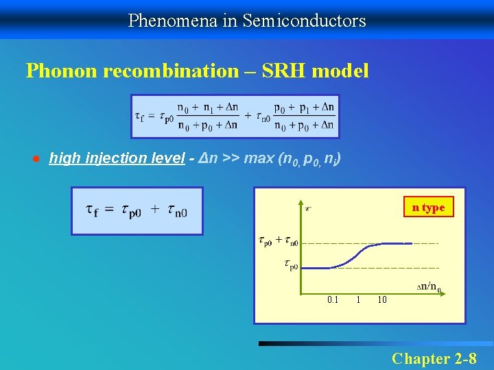
Phenomena in Semiconductors Phonon recombination – SRH model ● high injection level - Δn >> max (n 0, p 0, ni) n type 0. 1 1 10 Chapter 2 -8

Phenomena in Semiconductors Auger (impact) recombination hot electron-electron-hole process reeh = CAnn 2 p CAn – Auger recombination constant WC reeh W g WV for e-e-h process electron-hole process rehh = CApnp 2 CAp – Auger recombination constant for e-h-h process WC rehh Wg WV hot hole Chapter 2 -9
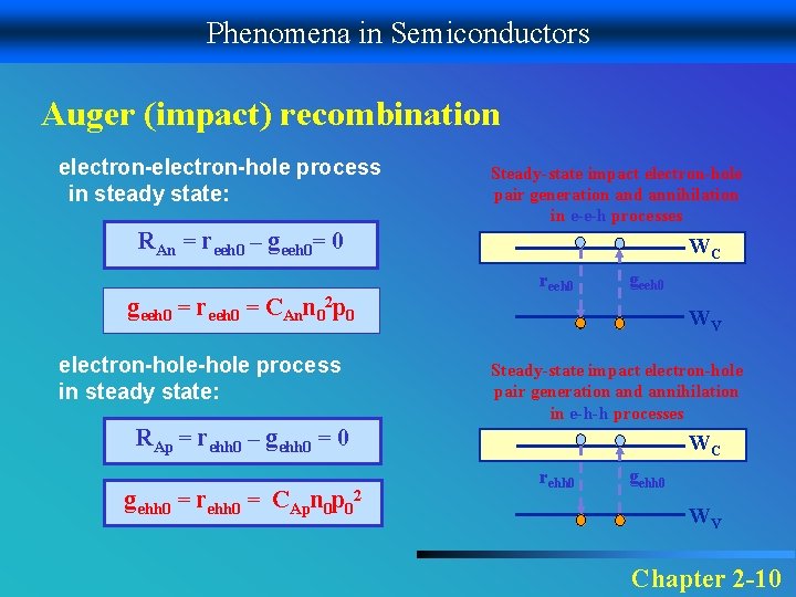
Phenomena in Semiconductors Auger (impact) recombination electron-hole process in steady state: Steady-state impact electron-hole pair generation and annihilation in e-e-h processes RAn = reeh 0 – geeh 0= 0 geeh 0 = reeh 0 = CAnn 02 p 0 electron-hole process in steady state: WC reeh 0 geeh 0 WV Steady-state impact electron-hole pair generation and annihilation in e-h-h processes RAp = rehh 0 – gehh 0 = 0 gehh 0 = rehh 0 = CApn 0 p 02 WC rehh 0 gehh 0 WV Chapter 2 -10
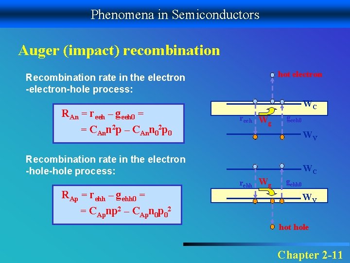
Phenomena in Semiconductors Auger (impact) recombination hot electron Recombination rate in the electron -electron-hole process: RAn = reeh – geeh 0 = = CAnn 2 p – CAnn 02 p 0 Recombination rate in the electron -hole process: RAp = rehh – gehh 0 = = CApnp 2 – CApn 0 p 02 WC reeh W g geeh 0 WV WC rehh Wg gehh 0 WV hot hole Chapter 2 -11
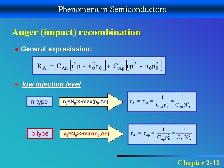
Phenomena in Semiconductors Auger (impact) recombination ● General expresission: ● low injection level n type n 0=ND>>max(p 0, Δn) p type p 0=NA>>max(n 0, Δn) Chapter 2 -12
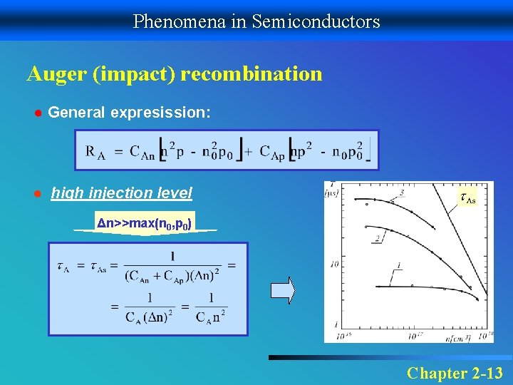
Phenomena in Semiconductors Auger (impact) recombination ● General expresission: ● high injection level Δn>>max(n 0, p 0) Chapter 2 -13
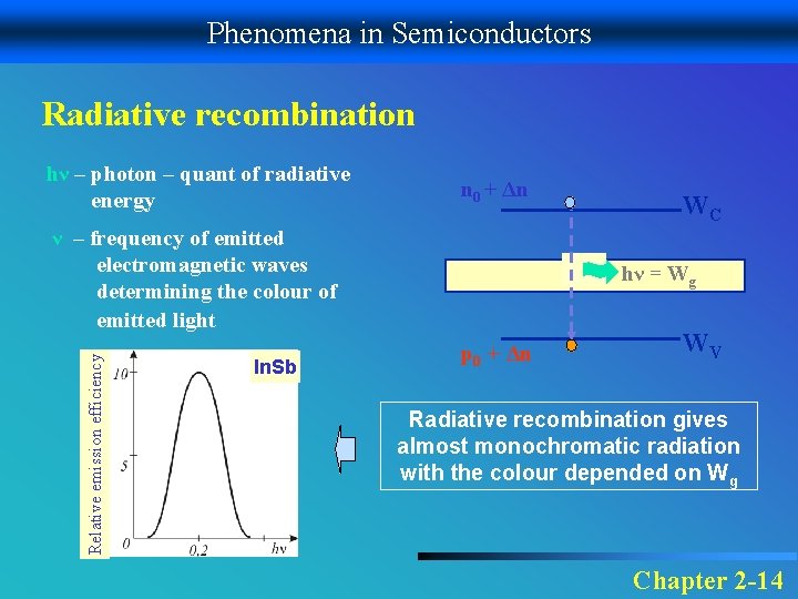
Phenomena in Semiconductors Radiative recombination hν – photon – quant of radiative energy n 0 + Δn Relative emission efficiency ν – frequency of emitted electromagnetic waves determining the colour of emitted light In. Sb WC hν = Wg p 0 + Δn WV Radiative recombination gives almost monochromatic radiation with the colour depended on Wg Chapter 2 -14

Phenomena in Semiconductors Surface recombination At the surface, the number of recombination centres responsible for phonon recombination is larger than in the whole volume due to the larger number of defects and outside agents interference. As result, in the border layer of semiconductor structure, the recombination rate, R(x) increases (R 2=var. ) in comparison to its value inside the structure where usually it is constant (R 1=const. ), R 1=const. R 2=var R(x) n 0 Chapter 2 -15
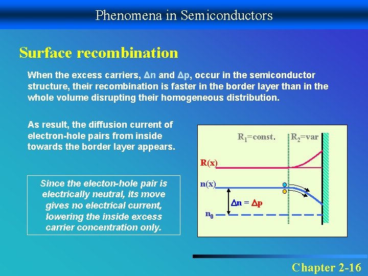
Phenomena in Semiconductors Surface recombination When the excess carriers, Δn and Δp, occur in the semiconductor structure, their recombination is faster in the border layer than in the whole volume disrupting their homogeneous distribution. As result, the diffusion current of electron-hole pairs from inside towards the border layer appears. R 1=const. R 2=var R(x) Since the electon-hole pair is electrically neutral, its move gives no electrical current, lowering the inside excess carrier concentration only. n(x) n = p n 0 Chapter 2 -16
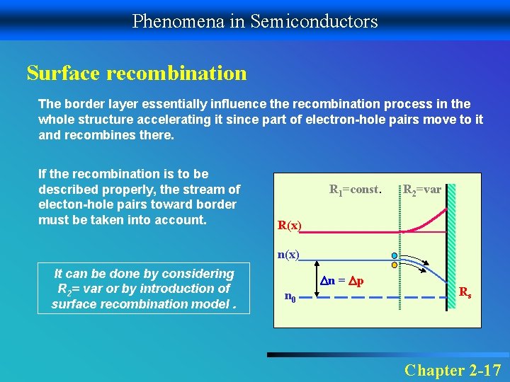
Phenomena in Semiconductors Surface recombination The border layer essentially influence the recombination process in the whole structure accelerating it since part of electron-hole pairs move to it and recombines there. If the recombination is to be described properly, the stream of electon-hole pairs toward border must be taken into account. R 1=const. R 2=var R(x) n(x) It can be done by considering R 2= var or by introduction of surface recombination model. n = p n 0 Rs Chapter 2 -17
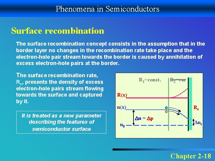
Phenomena in Semiconductors Surface recombination The surface recombination concept consists in the assumption that in the border layer no changes in the recombination rate take place and the electron-hole pair stream towards the border is caused by annihilation of excess electron-hole pairs at the border. The surface recombination rate, Rs, presents the density of excess electron-hole pairs stream flowing towards the surface and captured by it. It is treated as a new parameter describing the features of semiconductor surface R 1=const. R 2=var R(x) n(x) Rs n = p n 0 Δns Chapter 2 -18
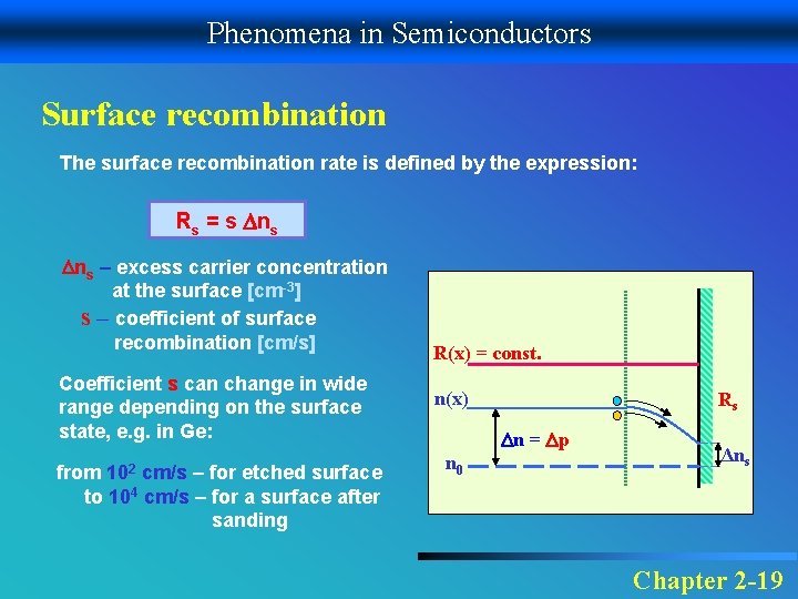
Phenomena in Semiconductors Surface recombination The surface recombination rate is defined by the expression: Rs = s ns ns – excess carrier concentration at the surface [cm-3] s – coefficient of surface recombination [cm/s] Coefficient s can change in wide range depending on the surface state, e. g. in Ge: 102 from cm/s – for etched surface to 104 cm/s – for a surface after sanding R(x) = const. n(x) Rs n = p n 0 Δns Chapter 2 -19
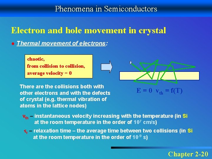
Phenomena in Semiconductors Electron and hole movement in crystal ● Thermal movement of electrons: chaotic, from collision to collision, average velocity = 0 There are the collisions both with other electrons and with the defects of crystal (e. g. thermal vibration of atoms in the lattice nodes) E = 0 vth = f(T) vth – instantaneous velocity increasing with the temperature (in Si at the room temperature in the order of 107 cm/s) r – relaxation time – the average time between two collisions (in Si at the room temperature in the order of 10 -9 s) Chapter 2 -20
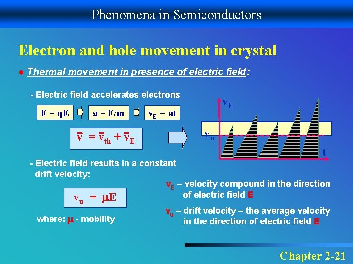
Phenomena in Semiconductors Electron and hole movement in crystal ● Thermal movement in presence of electric field: - Electric field accelerates electrons F = q. E a = F/m v = vth + v. E = at vu t - Electric field results in a constant drift velocity: v. E – velocity compound in the direction of electric field E v = m. E u where: m - mobility vu – drift velocity – the average velocity in the direction of electric field E Chapter 2 -21
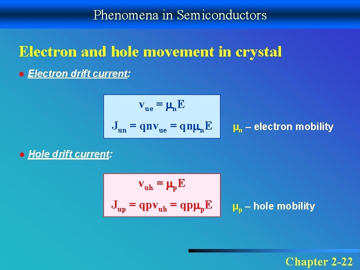
Phenomena in Semiconductors Electron and hole movement in crystal ● Electron drift current: vue = mn. E Jun = qnvue = qnmn. E µn – electron mobility ● Hole drift current: vuh = mp. E Jup = qpvuh = qpmp. E µp – hole mobility Chapter 2 -22
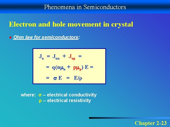
Phenomena in Semiconductors Electron and hole movement in crystal ● Ohm law for semiconductors: Ju = Jun + Jup = = q(nmn + pmp) E = = s E = E/ρ where: σ – electrical conductivity ρ – electrical resistivity Chapter 2 -23
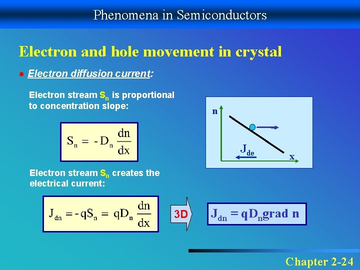
Phenomena in Semiconductors Electron and hole movement in crystal ● Electron diffusion current: Electron stream Sn is proportional to concentration slope: n Jde x Electron stream Sn creates the electrical current: 3 D Jdn = q. Dngrad n Chapter 2 -24
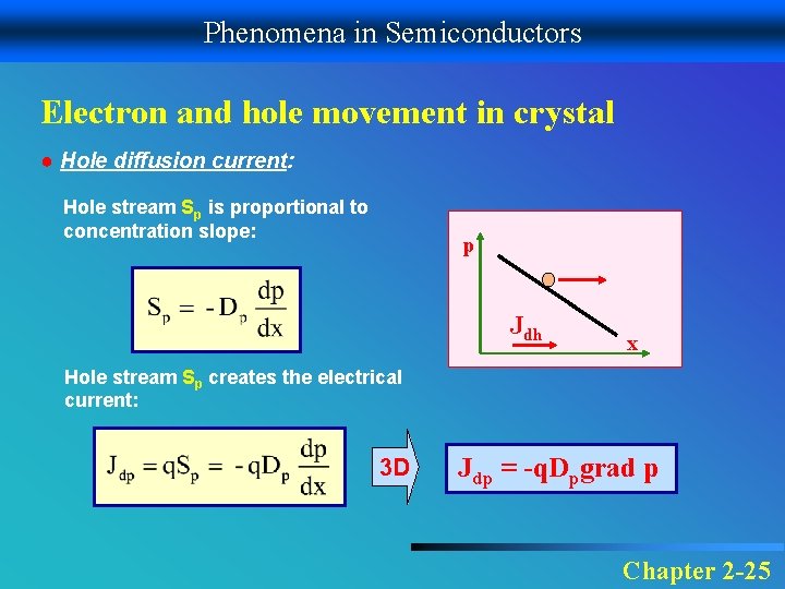
Phenomena in Semiconductors Electron and hole movement in crystal ● Hole diffusion current: Hole stream Sp is proportional to concentration slope: p n Jdh x Hole stream Sp creates the electrical current: 3 D Jdp = -q. Dpgrad p Chapter 2 -25
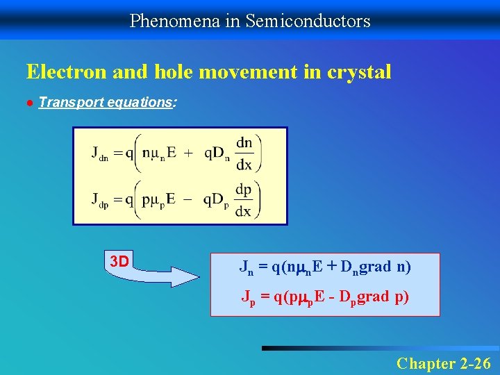
Phenomena in Semiconductors Electron and hole movement in crystal ● Transport equations: 3 D Jn = q(nmn. E + Dngrad n) Jp = q(pmp. E - Dpgrad p) Chapter 2 -26
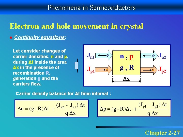
Phenomena in Semiconductors Electron and hole movement in crystal ● Continuity equations: Let consider changes of carrier densities, n and p, during Δt inside the area Δx in the presence of recombination R, generation g and the carriers flow. Jn 1 n, p Jn 2 Jp 1 g, R Jp 2 x Carrier density balance for Δt time interval : Chapter 2 -27
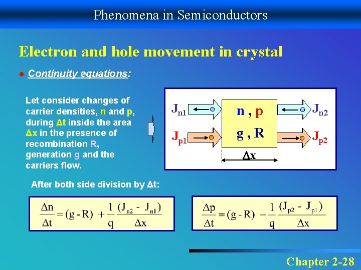
Phenomena in Semiconductors Electron and hole movement in crystal ● Continuity equations: Let consider changes of carrier densities, n and p, during Δt inside the area Δx in the presence of recombination R, generation g and the carriers flow. Jn 1 n, p Jn 2 Jp 1 g, R Jp 2 x After both side division by Δt: Chapter 2 -28
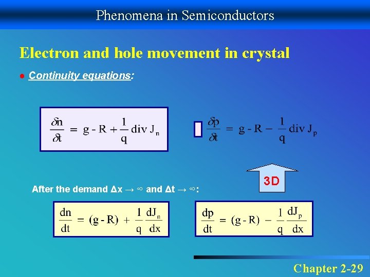
Phenomena in Semiconductors Electron and hole movement in crystal ● Continuity equations: After the demand Δx → ∞ and Δt → ∞: 3 D Chapter 2 -29
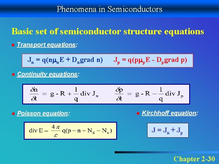
Phenomena in Semiconductors Basic set of semiconductor structure equations ● Transport equations: Jn = q(nmn. E + Dngrad n) Jp = q(pmp. E - Dpgrad p) ● Continuity equations: ● Poisson equation: ● Kirchhoff equation: J = Jn + Jp Chapter 2 -30
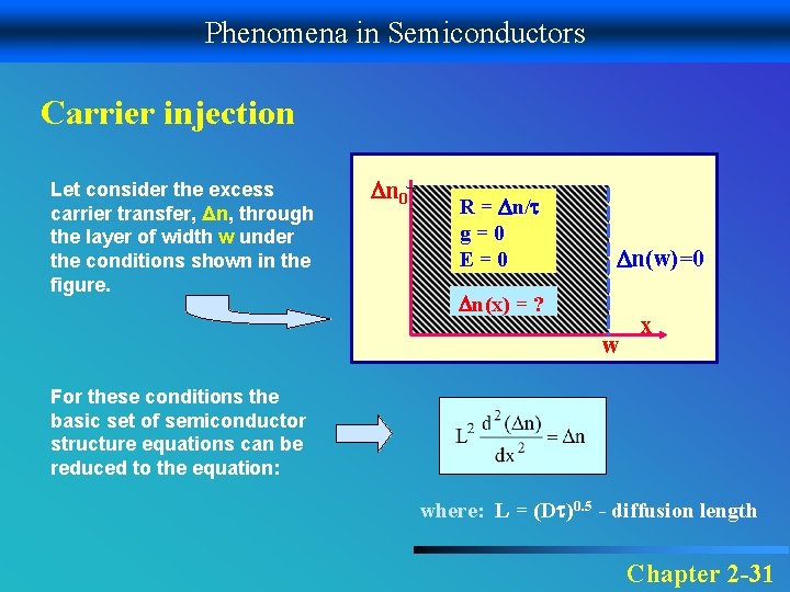
Phenomena in Semiconductors Carrier injection Let consider the excess carrier transfer, Δn, through the layer of width w under the conditions shown in the figure. n 0 R = n/ g=0 E=0 n(w)=0 n(x) = ? w x For these conditions the basic set of semiconductor structure equations can be reduced to the equation: where: L = (D )0. 5 - diffusion length Chapter 2 -31
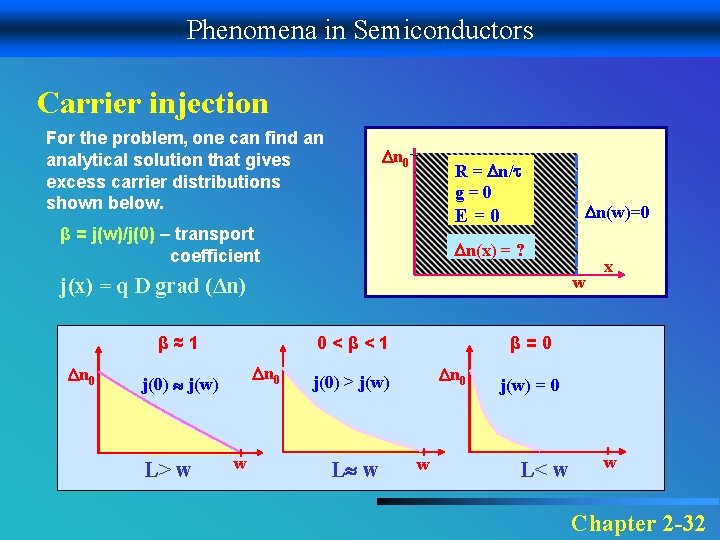
Phenomena in Semiconductors Carrier injection For the problem, one can find an analytical solution that gives excess carrier distributions shown below. n 0 R = n/ g=0 E=0 β = j(w)/j(0) – transport coefficient n(x) = ? w j(x) = q D grad (Δn) 0<β<1 β≈1 n 0 j(0) j(w) L> w w n(w)=0 β=0 n 0 j(0) > j(w) L w x w j(w) = 0 L< w w Chapter 2 -32
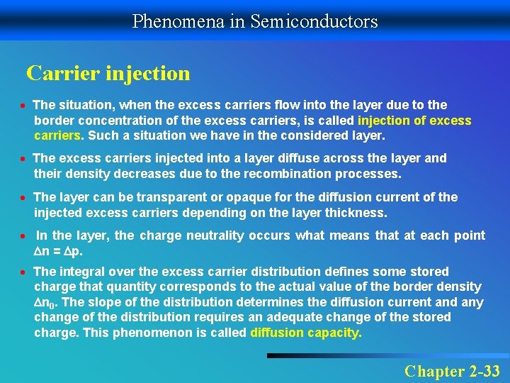
Phenomena in Semiconductors Carrier injection The situation, when the excess carriers flow into the layer due to the border concentration of the excess carriers, is called injection of excess carriers. Such a situation we have in the considered layer. The excess carriers injected into a layer diffuse across the layer and their density decreases due to the recombination processes. The layer can be transparent or opaque for the diffusion current of the injected excess carriers depending on the layer thickness. In the layer, the charge neutrality occurs what means that at each point n = p. The integral over the excess carrier distribution defines some stored charge that quantity corresponds to the actual value of the border density n 0. The slope of the distribution determines the diffusion current and any change of the distribution requires an adequate change of the stored charge. This phenomenon is called diffusion capacity. Chapter 2 -33
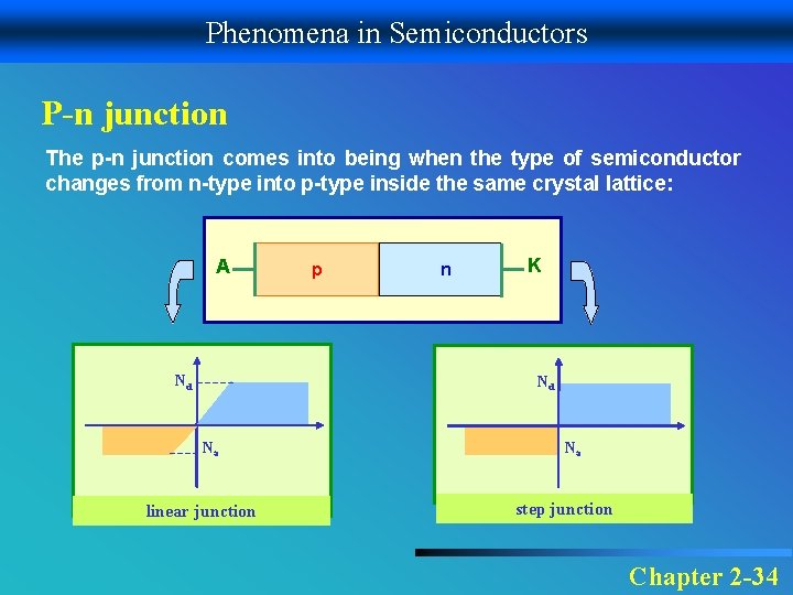
Phenomena in Semiconductors P-n junction The p-n junction comes into being when the type of semiconductor changes from n-type into p-type inside the same crystal lattice: A Nd p n K Nd Na linear junction Na step junction Chapter 2 -34
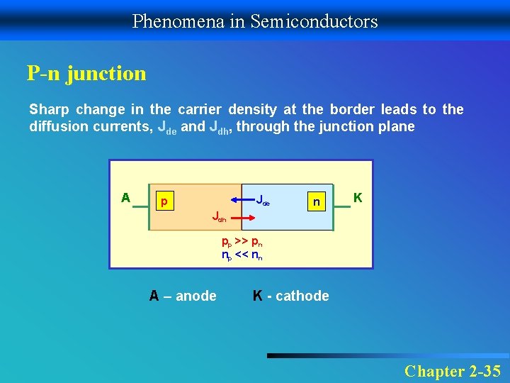
Phenomena in Semiconductors P-n junction Sharp change in the carrier density at the border leads to the diffusion currents, Jde and Jdh, through the junction plane A Jde p n K Jdh pp >> pn np << nn A – anode K - cathode Chapter 2 -35
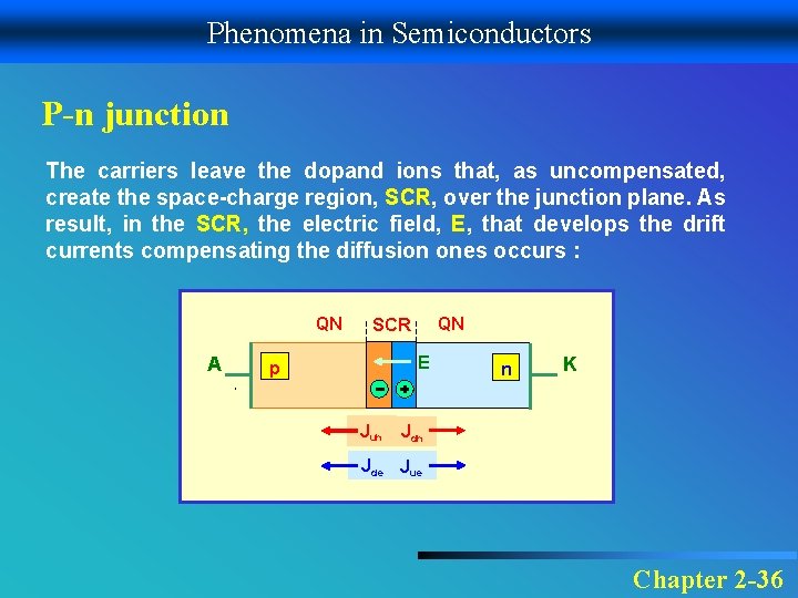
Phenomena in Semiconductors P-n junction The carriers leave the dopand ions that, as uncompensated, create the space-charge region, SCR, over the junction plane. As result, in the SCR, the electric field, E, that develops the drift currents compensating the diffusion ones occurs : QN A QN SCR E p Juh n K Jdh Jde Jue Chapter 2 -36
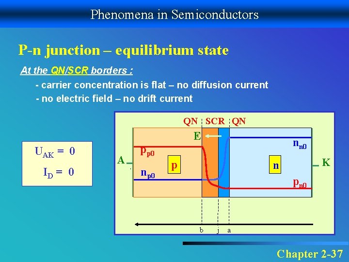
Phenomena in Semiconductors P-n junction – equilibrium state At the QN/SCR borders : - carrier concentration is flat – no diffusion current - no electric field – no drift current QN SCR QN E UAK = 0 ID = 0 A nn 0 pp 0 np 0 p K n pn 0 b j a Chapter 2 -37

Phenomena in Semiconductors P-n junction – equilibrium state In SCR area : - on the n-side Nd >> nn Qn = q(Nd + pn – nn) ≈ q. Nd - on the p-side Na >> pp Qp = q(- Na - np + pp) ≈ - q. Na on n-side: QN SCR QN E for x>a E increases linearly A nn 0 pp 0 np 0 p K n pn 0 b a Chapter 2 -38
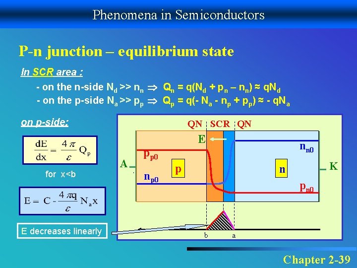
Phenomena in Semiconductors P-n junction – equilibrium state In SCR area : - on the n-side Nd >> nn Qn = q(Nd + pn – nn) ≈ q. Nd - on the p-side Na >> pp Qp = q(- Na - np + pp) ≈ - q. Na on p-side: QN SCR QN E for x<b E decreases linearly A nn 0 pp 0 np 0 p K n pn 0 b a Chapter 2 -39
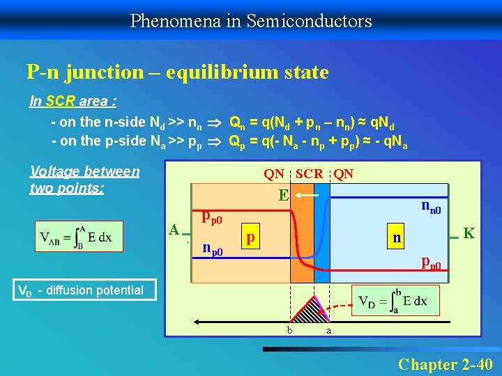
Phenomena in Semiconductors P-n junction – equilibrium state In SCR area : - on the n-side Nd >> nn Qn = q(Nd + pn – nn) ≈ q. Nd - on the p-side Na >> pp Qp = q(- Na - np + pp) ≈ - q. Na Voltage between two points: QN SCR QN E A nn 0 pp 0 np 0 p K n pn 0 VD - diffusion potential b a Chapter 2 -40
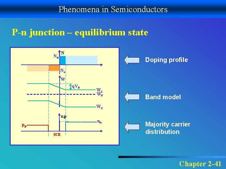
Phenomena in Semiconductors P-n junction – equilibrium state N Nd Doping profile Na W q. VD WC WF Band model WV n, p pp SCR nn Majority carrier distribution Chapter 2 -41
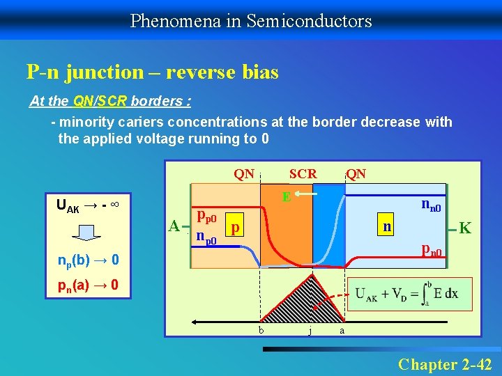
Phenomena in Semiconductors P-n junction – reverse bias At the QN/SCR borders : - minority cariers concentrations at the border decrease with the applied voltage running to 0 SCR QN QN E UAK → - ∞ A nn 0 pp 0 p np 0 n K pn 0 np(b) → 0 pn(a) → 0 b j a Chapter 2 -42
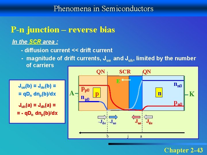
Phenomena in Semiconductors P-n junction – reverse bias In the SCR area : - diffusion current << drift current - magnitude of drift currents, Jue and Juh, limited by the number of carriers SCR QN QN Jue(b) = Jde(b) = = q. Dn dnp(b)/dx E A nn 0 pp 0 p np 0 n K pn 0 Juh(a) = Jdh(a) = = - q. Dn dnp(b)/dx Jue -Jde -Jue b j Jde a Chapter 2 -43
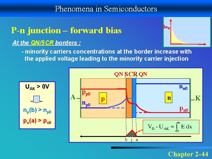
Phenomena in Semiconductors n 0 P-n junction – forward bias At the QN/SCR borders : - minority carriers concentrations at the border increase with the applied voltage leading to the minority carrier injection QN SCR QN UAK > 0 V A np(b) > np 0 pp 0 nn 0 n p K pn 0 pn(a) > pn 0 b j a Chapter 2 -44
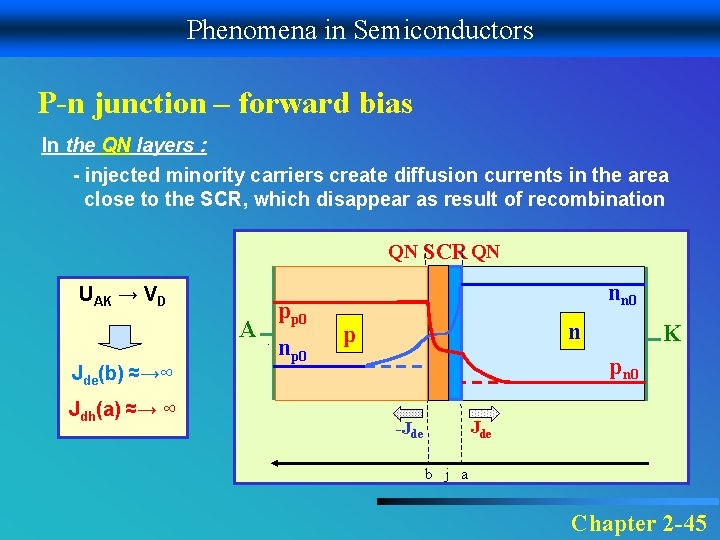
Phenomena in Semiconductors P-n junction – forward bias In the QN layers : - injected minority carriers create diffusion currents in the area close to the SCR, which disappear as result of recombination QN SCR QN UAK → VD A Jde(b) ≈→∞ Jdh(a) ≈→ ∞ pp 0 nn 0 n p K pn 0 Jde -Jde b j a Chapter 2 -45
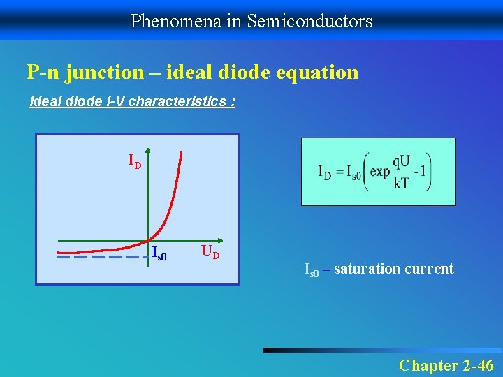
Phenomena in Semiconductors P-n junction – ideal diode equation Ideal diode I-V characteristics : ID Is 0 UD Is 0 – saturation current Chapter 2 -46
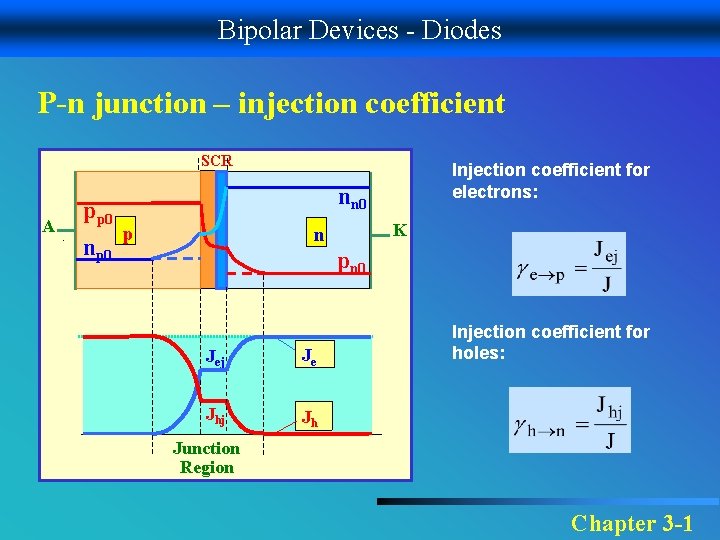
Bipolar Devices - Diodes P-n junction – injection coefficient SCR A pp 0 np 0 Injection coefficient for electrons: nn 0 p K n pn 0 Jej Je Jhj Jh Injection coefficient for holes: Junction Region Chapter 3 -1
- Slides: 48