Semiconductor Devices Prof Zbigniew Lisik Department of Semiconductor
Semiconductor Devices Prof. Zbigniew Lisik Department of Semiconductor and Optoelectronics Devices room: 116 e-mail: zbigniew. lisik@p. lodz. pl Chapter 3 Bipolar devices IFE T&CS
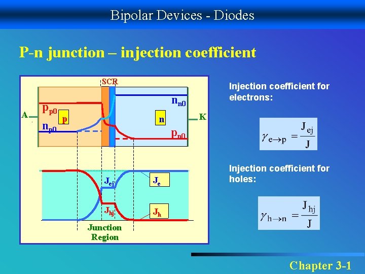
Bipolar Devices - Diodes P-n junction – injection coefficient SCR A pp 0 np 0 Injection coefficient for electrons: nn 0 p K n pn 0 Jej Je Jhj Jh Injection coefficient for holes: Junction Region Chapter 3 -1
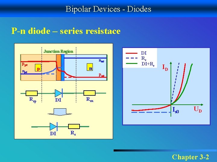
Bipolar Devices - Diodes P-n diode – series resistace Junction Region nn 0 pp 0 n p np 0 DI Rs DI+Rs ID pn 0 Rsp Rsn DI Is 0 DI UD Rs Chapter 3 -2
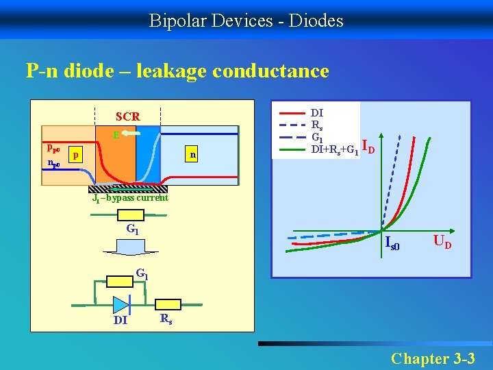
Bipolar Devices - Diodes P-n diode – leakage conductance SCR E pp 0 n p DI Rs Gl DI+Rs+Gl ID Jl – bypass current Gl Is 0 UD Gl DI Rs Chapter 3 -3
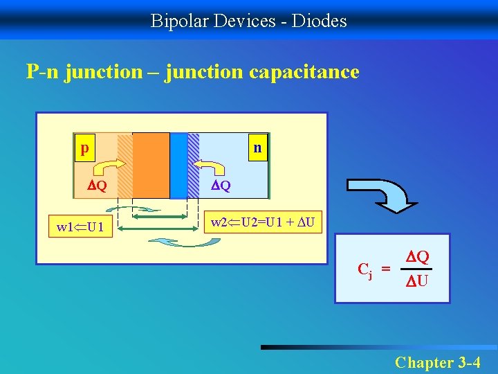
Bipolar Devices - Diodes P-n junction – junction capacitance p Q w 1 U 1 n Q w 2 U 2=U 1 + DU Q Cj = U Chapter 3 -4
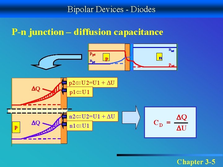
Bipolar Devices - Diodes P-n junction – diffusion capacitance pp 0 np 0 Q p Q nn 0 p n pn 0 p 2 U 2=U 1 + DU p 1 U 1 n 2 U 2=U 1 + DU n 1 U 1 Q CD = U Chapter 3 -5
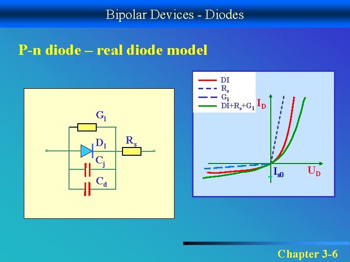
Bipolar Devices - Diodes P-n diode – real diode model DI Rs Gl DI+Rs+Gl ID Gl DI Cj Cd Rs Is 0 UD Chapter 3 -6
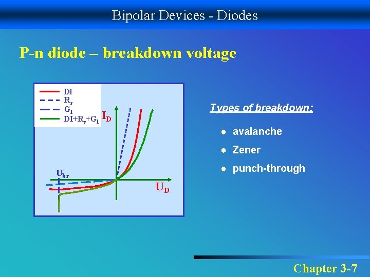
Bipolar Devices - Diodes P-n diode – breakdown voltage DI Rs Gl DI+Rs+Gl ID Types of breakdown: ● avalanche ● Zener ● punch-through Ubr UD Chapter 3 -7
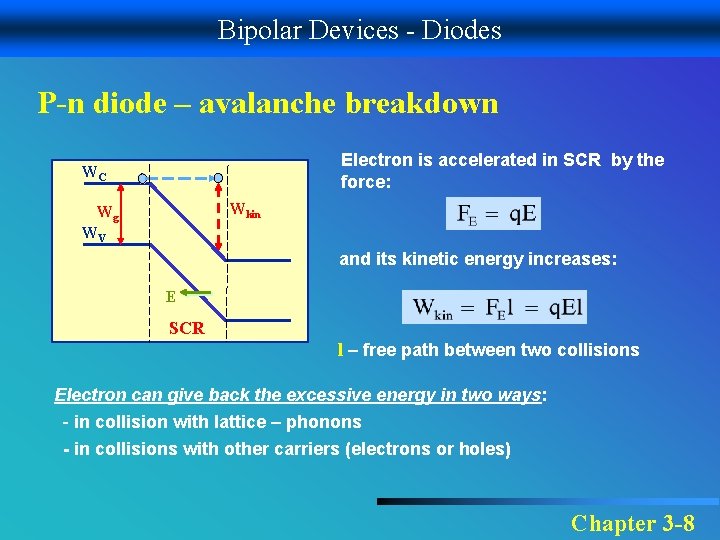
Bipolar Devices - Diodes P-n diode – avalanche breakdown Electron is accelerated in SCR by the force: WC Wkin Wg WV and its kinetic energy increases: E SCR l – free path between two collisions Electron can give back the excessive energy in two ways: - in collision with lattice – phonons - in collisions with other carriers (electrons or holes) Chapter 3 -8
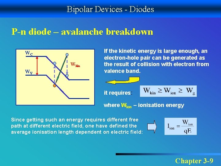
Bipolar Devices - Diodes P-n diode – avalanche breakdown WC Wkin WV If the kinetic energy is large enough, an electron-hole pair can be generated as the result of collision with electron from valence band. it requires: where Wion – ionisation energy Since getting such an energy requires different free path at different electric field, one have defined the average ionisation length dependent on electric field: Chapter 3 -9
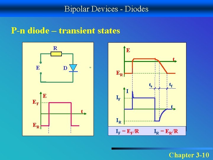
Bipolar Devices - Diodes P-n diode – transient states R E t E EF D ER E IF I tf t t ER ts IR IF = EF/R IR = ER/R Chapter 3 -10
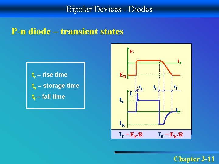
Bipolar Devices - Diodes P-n diode – transient states E t tr – rise time ER ts – storage time tf – fall time IF I tr ts tf t IR IF = EF/R IR = ER/R Chapter 3 -11
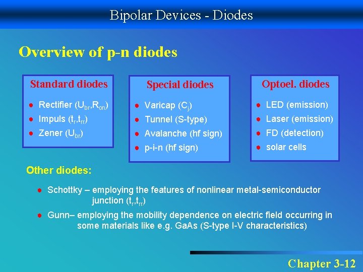
Bipolar Devices - Diodes Overview of p-n diodes Standard diodes Special diodes Optoel. diodes ● Rectifier (Ubr, Ron) ● Varicap (Cj) ● LED (emission) ● Impuls (tr, trr) ● Tunnel (S-type) ● Laser (emission) ● Zener (Ubr) ● Avalanche (hf sign) ● FD (detection) ● p-i-n (hf sign) ● solar cells Other diodes: ● Schottky – employing the features of nonlinear metal-semiconductor junction (tr, trr) ● Gunn– employing the mobility dependence on electric field occurring in some materials like e. g. Ga. As (S-type I-V characteristics) Chapter 3 -12
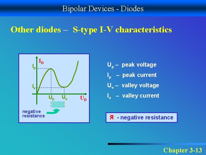
Bipolar Devices - Diodes Other diodes – S-type I-V characteristics Ip ID Up – peak voltage Ip – peak current Uv – valley voltage Iv Up negative resistance Uv UD Iv – valley current Я - negative resistance Chapter 3 -13
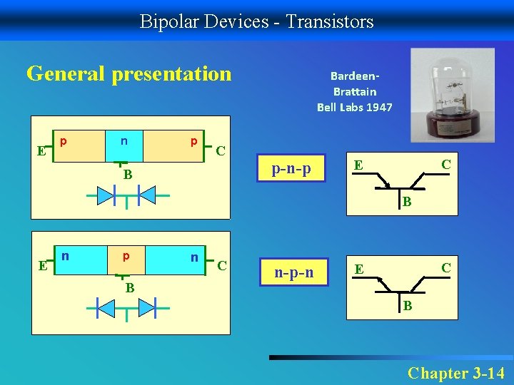
Bipolar Devices - Transistors General presentation E p n p C B Bardeen. Brattain Bell Labs 1947 p-n-p C E B E n p B n C n-p-n C E B Chapter 3 -14
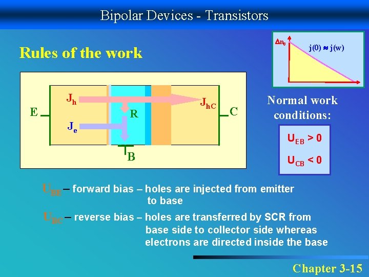
Bipolar Devices - Transistors n 0 Rules of the work E Jh Je Jh. C R C j(0) j(w) Normal work conditions: UEB > 0 B UCB < 0 UBE – forward bias – holes are injected from emitter to base UBC – reverse bias – holes are transferred by SCR from base side to collector side whereas electrons are directed inside the base Chapter 3 -15
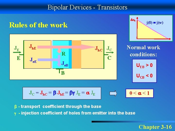
Bipolar Devices - Transistors n 0 Rules of the work JE Jh. E E Je. E R Jh. C JC Je. B C Normal work conditions: UEB > 0 B JC = Jh. C = Jh. E = JE j(0) j(w) UCB < 0 0< <1 β - transport coefficient through the base - injection coefficient of holes from emitter into the base Chapter 3 -16
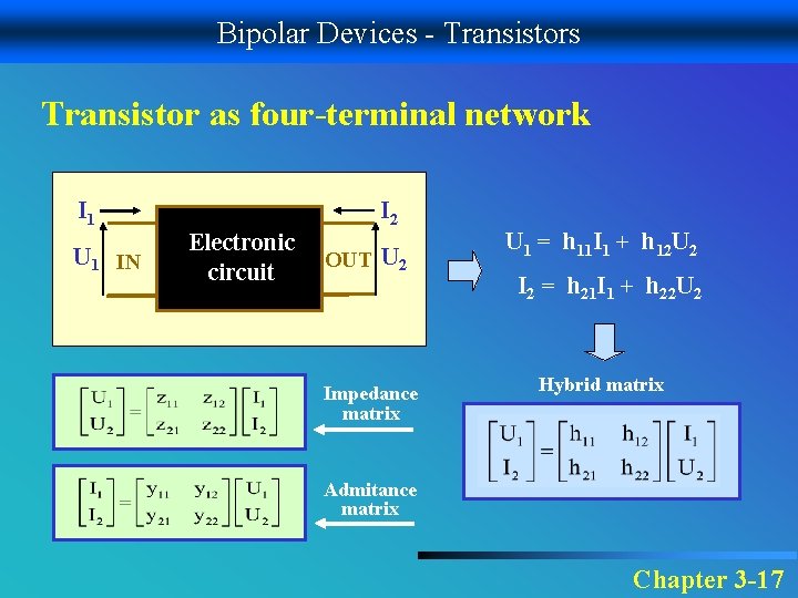
Bipolar Devices - Transistors Transistor as four-terminal network I 1 U 1 IN I 2 Electronic circuit OUT U 2 Impedance matrix U 1 = h 11 I 1 + h 12 U 2 I 2 = h 21 I 1 + h 22 U 2 Hybrid matrix Admitance matrix Chapter 3 -17
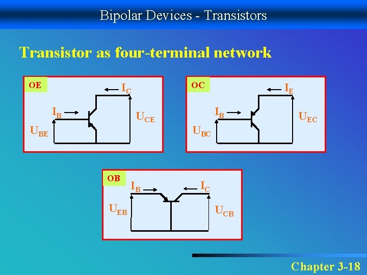
Bipolar Devices - Transistors Transistor as four-terminal network OE OC IC IB UCE UBE OB UEB IB IE IB UBC UEC IC UCB Chapter 3 -18
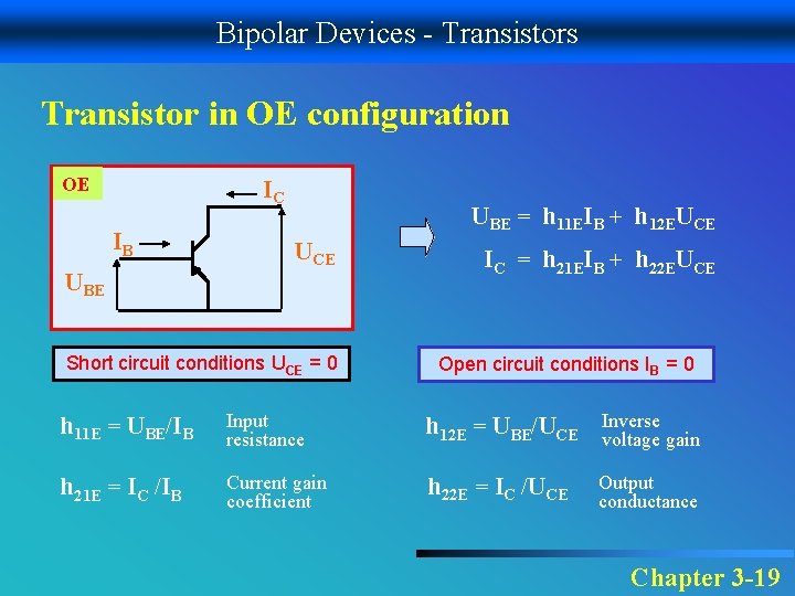
Bipolar Devices - Transistors Transistor in OE configuration OE IC IB UBE = h 11 EIB + h 12 EUCE Short circuit conditions UCE = 0 IC = h 21 EIB + h 22 EUCE Open circuit conditions IB = 0 h 11 E = UBE/IB Input resistance h 12 E = UBE/UCE Inverse h 21 E = IC /IB Current gain coefficient h 22 E = IC /UCE voltage gain Output conductance Chapter 3 -19
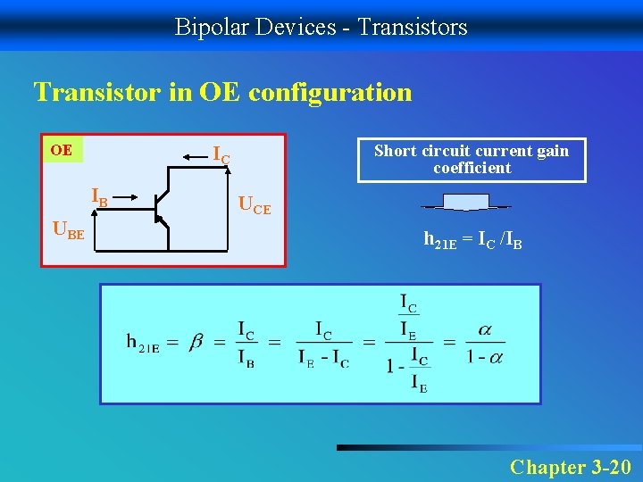
Bipolar Devices - Transistors Transistor in OE configuration OE IB UBE Short circuit current gain coefficient IC UCE h 21 E = IC /IB Chapter 3 -20
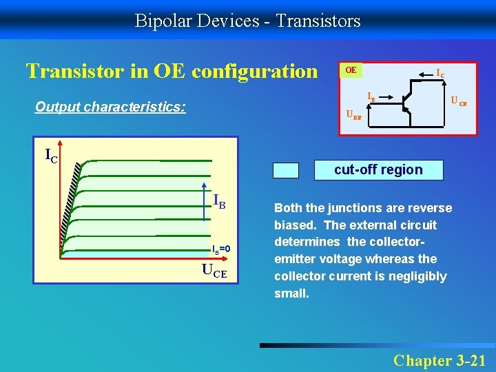
Bipolar Devices - Transistors Transistor in OE configuration OE IC IB Output characteristics: UCE UBE IC cut-off region IB IB=0 UCE Both the junctions are reverse biased. The external circuit determines the collectoremitter voltage whereas the collector current is negligibly small. Chapter 3 -21
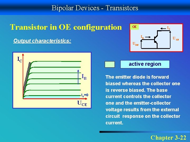
Bipolar Devices - Transistors Transistor in OE configuration OE IC IB Output characteristics: UCE UBE IC active region IB IB=0 UCE The emitter diode is forward biased whereas the collector one is reverse biased. The base current controls the collector one and the emitter-collector voltage results from the external circuit response on the collector current. Chapter 3 -22
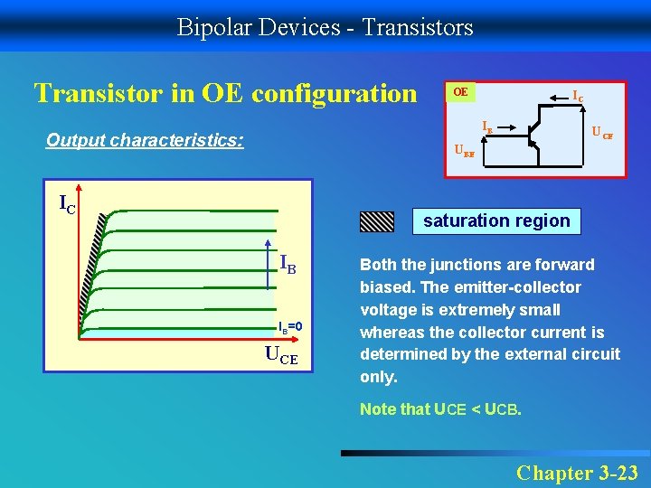
Bipolar Devices - Transistors Transistor in OE configuration OE IC IB Output characteristics: UCE UBE IC saturation region IB IB=0 UCE Both the junctions are forward biased. The emitter-collector voltage is extremely small whereas the collector current is determined by the external circuit only. Note that UCE < UCB. Chapter 3 -23
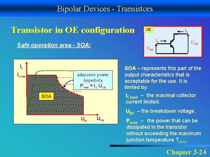
Bipolar Devices - Transistors Transistor in OE configuration IC IB Safe operation area - SOA: UCE UBE IC admissive power hyperbola Pmax = IC UCE ICmax OE SOA – represents this part of the output characteristics that is acceptable for the use. It is limited by: ICmax – the maximal collector current limited. SOA Ubr – the breakdown voltage, Ubr UCE Pmax – the power that can be dissipated in the transistor without exceeding the maximum junction temperature Tjmax Chapter 3 -24
- Slides: 25