Semiconductor Devices Metalsemiconductor junction Rectifier Schottky contact or
- Slides: 20

Semiconductor Devices Ø Metal-semiconductor junction Ø Rectifier (Schottky contact or Schottky barrier) Ø Ohmic contact Ø p – n rectifier Ø Zener diode Ø Photodiode (solar cell) Ø Tunnel diode Ø Transistor Ø Other devices based on semiconductors (for hybrid circuits) Ø Resistor Ø Isolator Ø Capacitor 1

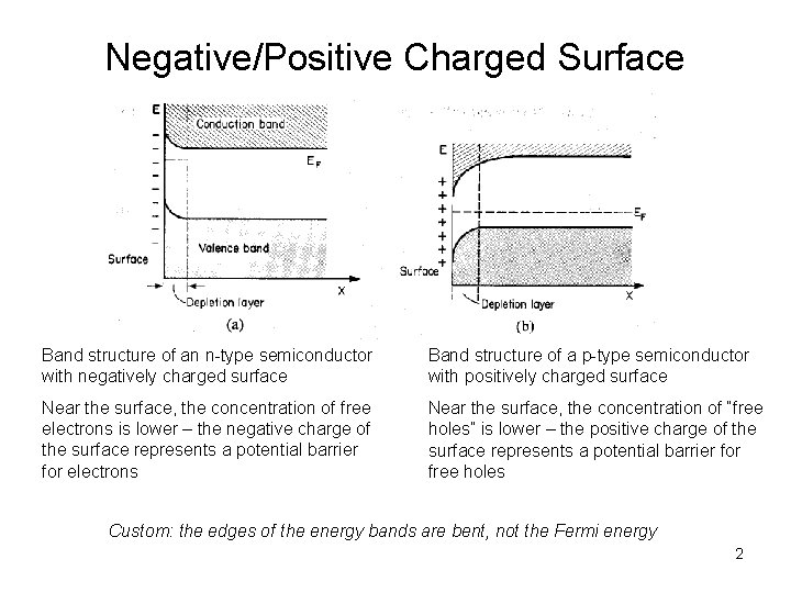
Negative/Positive Charged Surface Band structure of an n-type semiconductor with negatively charged surface Band structure of a p-type semiconductor with positively charged surface Near the surface, the concentration of free electrons is lower – the negative charge of the surface represents a potential barrier for electrons Near the surface, the concentration of “free holes” is lower – the positive charge of the surface represents a potential barrier for free holes Custom: the edges of the energy bands are bent, not the Fermi energy 2

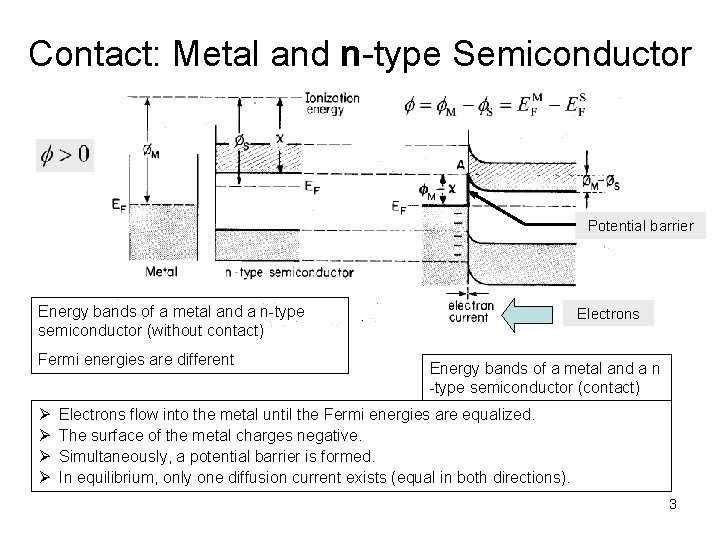
Contact: Metal and n-type Semiconductor Potential barrier Energy bands of a metal and a n-type semiconductor (without contact) Fermi energies are different Ø Ø Electrons Energy bands of a metal and a n -type semiconductor (contact) Electrons flow into the metal until the Fermi energies are equalized. The surface of the metal charges negative. Simultaneously, a potential barrier is formed. In equilibrium, only one diffusion current exists (equal in both directions). 3

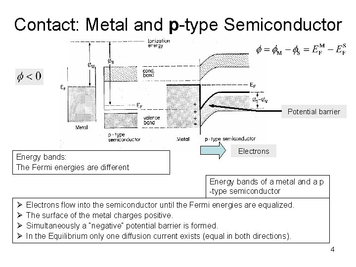
Contact: Metal and p-type Semiconductor Potential barrier Energy bands: The Fermi energies are different Electrons Energy bands of a metal and a p -type semiconductor Ø Ø Electrons flow into the semiconductor until the Fermi energies are equalized. The surface of the metal charges positive. Simultaneously a “negative” potential barrier is formed. In the Equilibrium only one diffusion current exists (equal in both directions). 4

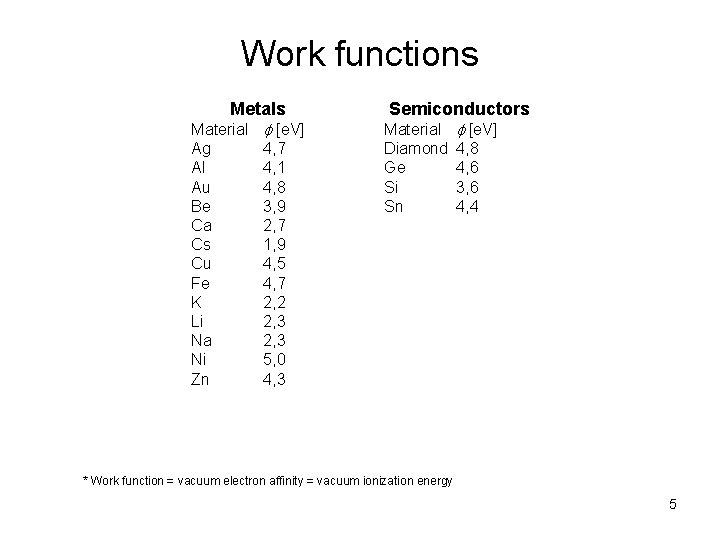
Work functions Metals Material Ag Al Au Be Ca Cs Cu Fe K Li Na Ni Zn [e. V] 4, 7 4, 1 4, 8 3, 9 2, 7 1, 9 4, 5 4, 7 2, 2 2, 3 5, 0 4, 3 Semiconductors Material Diamond Ge Si Sn [e. V] 4, 8 4, 6 3, 6 4, 4 * Work function = vacuum electron affinity = vacuum ionization energy 5

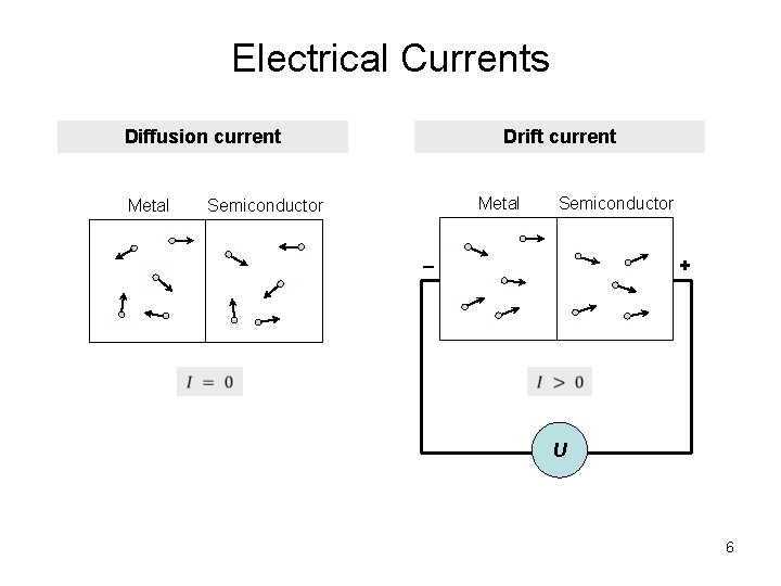
Electrical Currents Diffusion current Metal Drift current Metal Semiconductor – + U 6

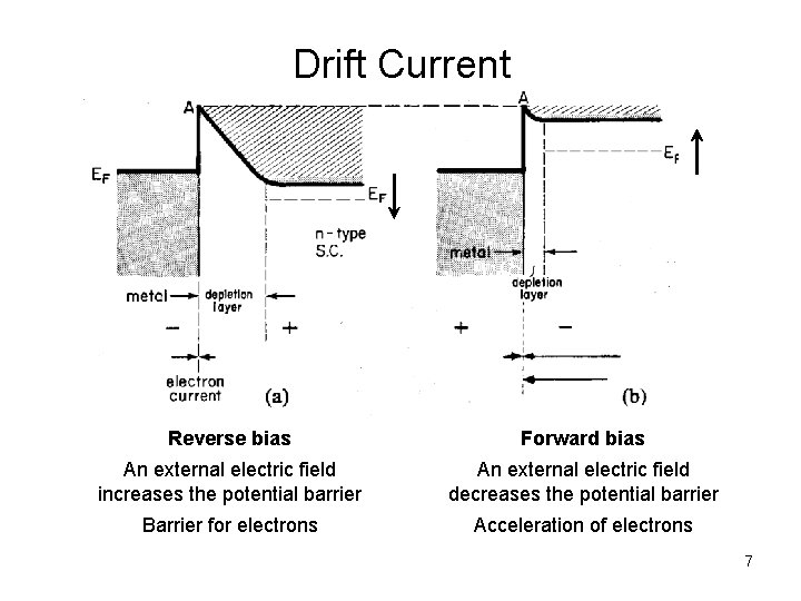
Drift Current Reverse bias Forward bias An external electric field increases the potential barrier An external electric field decreases the potential barrier Barrier for electrons Acceleration of electrons 7

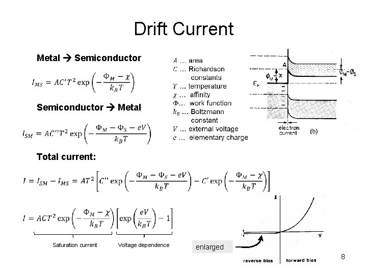
Drift Current Metal Semiconductor Metal Total current: Saturation current Voltage dependence enlarged 8

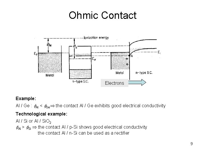
Ohmic Contact Electrons Example: Al / Ge : Al < Ge the contact Al / Ge exhibits good electrical conductivity Technological example: Al / Si or Al / Si. O 2 Al > Si the contact Al / p-Si shows good electrical conductivity the contact Al / n-Si can be used as a rectifier 9

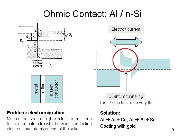
Ohmic Contact: Al / n-Si n-semiconductor n+-film metal Electron current Quantum tunneling The n+ slab has to be very thin. Problem: electromigration Material transport at high electric currents, due to the momentum transfer between conducting electrons and atoms or ions of the solid Solution: Al + Cu, Al + Si Coating with gold 10

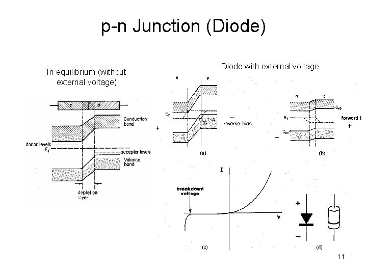
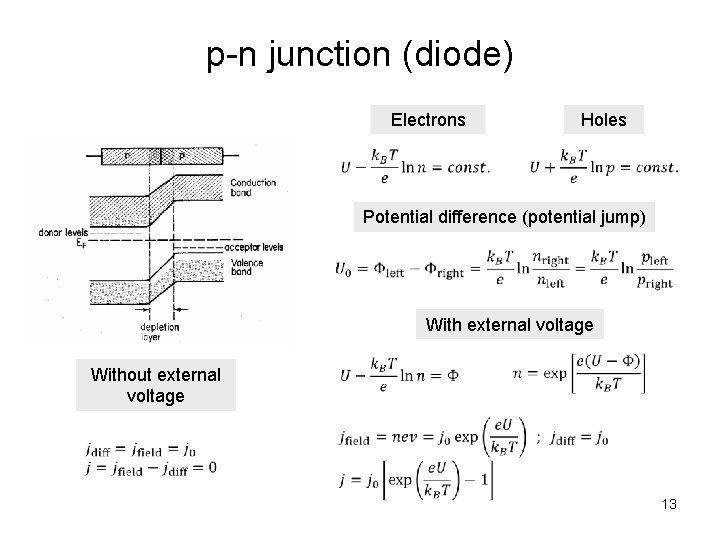
p-n Junction (Diode) In equilibrium (without external voltage) Diode with external voltage 11

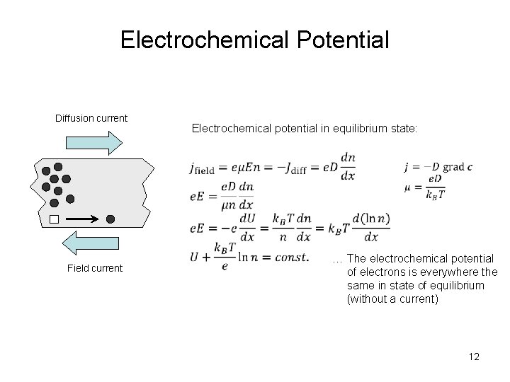
Electrochemical Potential Diffusion current Electrochemical potential in equilibrium state: Field current … The electrochemical potential of electrons is everywhere the same in state of equilibrium (without a current) 12

p-n junction (diode) Electrons Holes Potential difference (potential jump) With external voltage Without external voltage 13

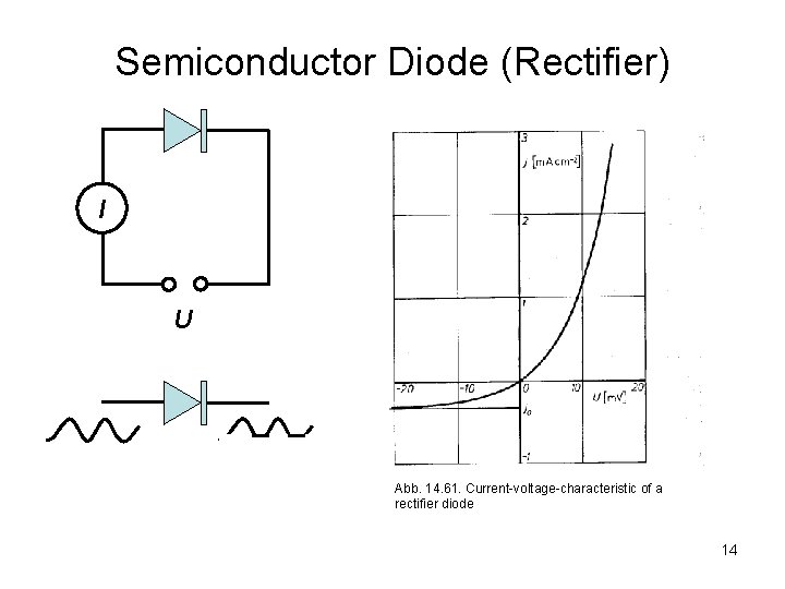
Semiconductor Diode (Rectifier) I U Abb. 14. 61. Current-voltage-characteristic of a rectifier diode 14

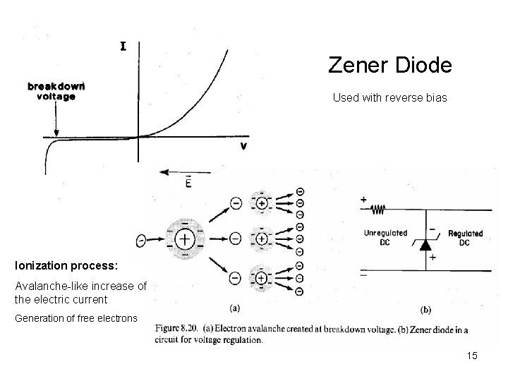
Zener Diode Used with reverse bias Ionization process: Avalanche-like increase of the electric current Generation of free electrons 15

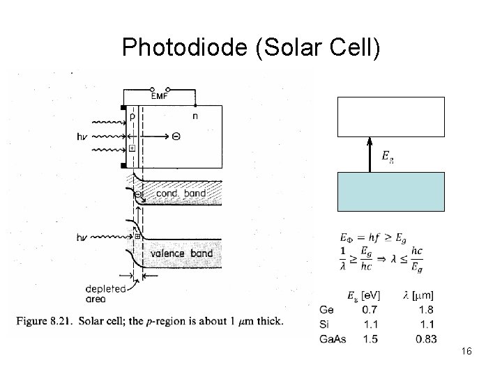
Photodiode (Solar Cell) 16

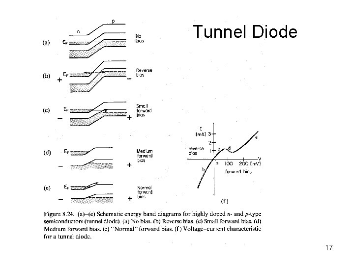
Tunnel Diode 17

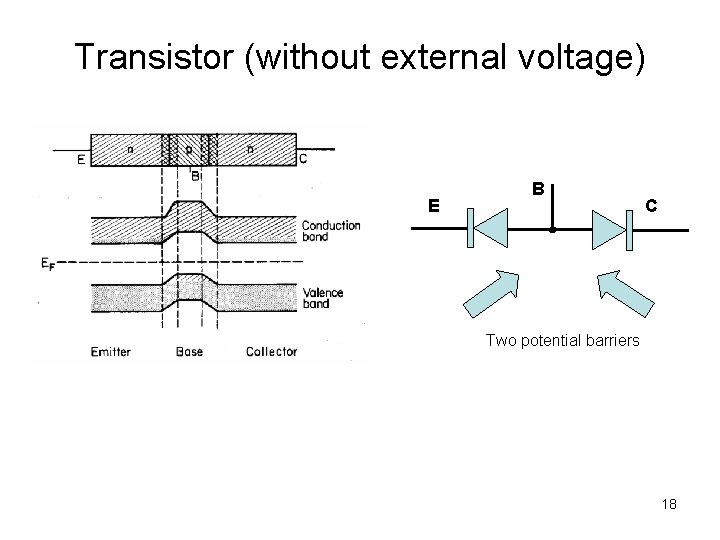
Transistor (without external voltage) E B C Two potential barriers 18

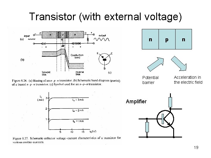
Transistor (with external voltage) n Potential barrier p n Acceleration in the electric field Amplifier 19

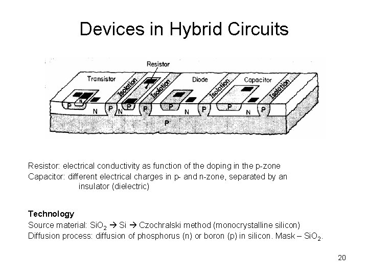
Devices in Hybrid Circuits Resistor: electrical conductivity as function of the doping in the p-zone Capacitor: different electrical charges in p- and n-zone, separated by an insulator (dielectric) Technology Source material: Si. O 2 Si Czochralski method (monocrystalline silicon) Diffusion process: diffusion of phosphorus (n) or boron (p) in silicon. Mask – Si. O 2. 20