Semiconductor Devices HVIC 1 POWER MOSFETs 2 INSULATED


 이기는 경영! 악착같이, 될때까지, 끝까지! 2/47")


 이기는")


 이기는")


 = maximum permissible gate-source voltage. • If VGS >VGS(max)")

 이기는")
 •")
 이기는")
 Outline • Construction and I-V characteristics • Physical operation")
 1. Switching speed, peak current capability, ease of drive,")
")


 Low voltage static losses are due")


 maximum IDS allowed by metal connections Current limited by RDS,")
- Slides: 48
Semiconductor Devices & HVIC 1. POWER MOSFETs 2. INSULATED GATE BIPOLAR TRANSISTORS 3. FAST RECOVERY DIODE 4. HIGH VOLTAGE ICs 2004. 02. 28 최 동 찬 (East. Chan) /부품 연구소 Power Part
Power MOSFETs Outline • Construction of power MOSFETs • Physical operations of MOSFETs • Power MOSFET switching Characteristics • Factors limiting operating specifications of MOSFET 이기는 경영! 악착같이, 될때까지, 끝까지! 1/47
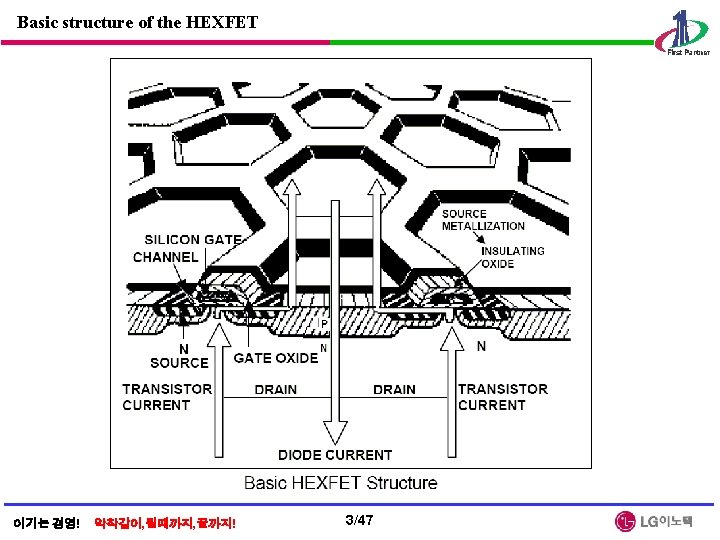
Multi-cell Vertical Diffused Power MOSFET (VDMOS) 이기는 경영! 악착같이, 될때까지, 끝까지! 2/47
Important Structural Features of VDMOS accumulation layer 1. Parasitic npn BJT. Held in cutoff by body-source short 2. Integral anti-parallel pn diode. 3. Extension of gate metallization over drain drift region. → Field plate and accumulation layer functions. 4. Division of source into many small areas connected electrically in parallel. Maximizes gate width-to-channel length ratio in order to increase gain. 5. Lightly doped drain drift region. Determines blocking voltage rating. 이기는 경영! 악착같이, 될때까지, 끝까지! 4/47
MOSFET I-V Characteristics • Cutoff - The drain-source voltage to avoid breakdown voltage BVDSS must be larger than the applied drain-source voltage to avid breakdown and the attendant high power dissipation. • Ohmic - The power dissipation can be kept within reasonable bounds by minimizing VDS(ON) even if the drain current is fairly large. • Active - The drain current is independent of the VDS & depends on only on the Vgs. 이기는 경영! 악착같이, 될때까지, 끝까지! 5/47
Example : Datasheet of FQA 62 N 25 C (250 V N-Channel MOSFET) 이기는 경영! 악착같이, 될때까지, 끝까지! 6/47
The Field Effect - Basis of MOSFET Operation ( VGG 1 < VGG 2 < VGG 3 ) • When a small positive gate-source voltage is applied to the capacitor structure. - The positive charge & equal negative charge are the both side of the gate oxide. - Repel the majority-carrier holes , thus exposes the negatively charged acceptor, thus creating a depletion region. • Further increases in Vgs : - The depletion layer to grow in thickness & additional negative charge. - Begins to attract free electrons as well as repelling free holes. - Electron-hole generation. • The layer of free electrons at the interface will be highly conducting and will have all the properties of an n-type semiconductor. → inversion layer : conductive path & channel between n+ drain and source. • The threshold voltage is inversely proportional to - Oxide capacitance per unit area tox = oxide thickness 이기는 경영! 악착같이, 될때까지, 끝까지! 7/47
MOSFET Capacitances Determining Switching Speed • Gate-source capacitance Cgs approximately constant and independent of applied voltages. • Gate-drain capacitance Cgd varies with applied voltage. Variation due to growth of depletion layer thickness until inversion layer is formed. • Drain-source capacitance Cds doesn’t materially affect any of the switching characteristics or waveforms. 이기는 경영! 악착같이, 될때까지, 끝까지! 8/47
Equivalent circuit & MOSFET Capacitances Determining Switching Speed • That the capacitance Cgs , Cgd & Cds are not constant but vary with the voltage across them because part of the capacitance is contributed by depletion layers. • The most Significant change in capacitance occurs in Cgd because the voltage change across it, vds, is much larger than the voltage change across Cgs. • For approximate calculations of switching waveform - Cgd is approximated by the two discrete values Cgd 1 & Cgd 2 with the change in value occurring at vds=vgs where the MOSFET is either entering or leaving the ohmic region - The gate-source capacitance will be assumed to be constant. 이기는 경영! 악착같이, 될때까지, 끝까지! 9/47
Example : Datasheet of FQA 62 N 25 C (250 V N-Channel MOSFET) 이기는 경영! 악착같이, 될때까지, 끝까지! 10/47
A MOSFET being turned on by a driver in a clamped inductive load • The gate-source capacitance Cgs is total value of capacitance that needs to be first charged to a critical threshold voltage level Vgs(th), before drain current can begin to flow. • The gate-drain capacitance Cgd (‘miller’ capacitance) between the gate electrode and the N-drift drain region contributes most to the switching speed limitation of the MOSFETs. • The rate of rise of voltage, Vgs, over Gate and Source terminals of the MOSFET is governed by value of the total resistance in series (Rdr+RGext+RGint) and total effective value of capacitance (Cgs+Cgd). • Rgext is the resistance one generally puts in series with the Gate of a MOSFET to control the turnon and turn-off speed of the MOSFET. 이기는 경영! 악착같이, 될때까지, 끝까지! 11/47
A MOSFET being turned on by a driver in a clamped inductive load • Free-wheeling diode assumed to be ideal. (no reverse recovery current). 이기는 경영! 악착같이, 될때까지, 끝까지! 12/47
A MOSFET being turned on by a driver in a clamped inductive load • Free-wheeling diode assumed to be ideal. (no reverse recovery current). 이기는 경영! 악착같이, 될때까지, 끝까지! 13/47
A MOSFET being turned off by a driver in a clamped inductive load • Assume ideal freewheeling diode. • Essentially the inverse of the turn-on process. • Model qualitatively using the same equivalent circuits as for turn-on. Simply use correct driving voltages and initial conditions 이기는 경영! 악착같이, 될때까지, 끝까지! 14/47
d. V/dt Limits to Prevent Parasitic BJT Turn-on • The parasitic BJT might be turned on by a fast-rising drain-source voltage (10, 000 V/μs). - Down the switching speed (∵ large RG) - Smaller values of turn-off gate drive. • For mechanism of possible destruction of MOSFETs used in a bridge configuration : - Prevented using diodes DL+ and DL- instead of directly connecting freewheeling diode Df+ and Df- to the MOSFET drains. 이기는 경영! 악착같이, 될때까지, 끝까지! 15/47
Maximum Gate-Source Voltage • VGS(max) = maximum permissible gate-source voltage. • If VGS >VGS(max) rupture of gate oxide by large electric fields possible. • Gate oxide typically 1000 anstroms thick • Typical VGS(max) : 20 -30 V • Static charge on gate conductor can rupture gate oxide • Handle MOSFETs with care (ground yourself before handling device) • Place anti-parallel connected Zener diodes between gate and source as a protective measure. Example : Datasheet of FQA 62 N 25 C (250 V N-Channel MOSFET) 이기는 경영! 악착같이, 될때까지, 끝까지! 16/47
MOSFET Breakdown Voltage • BVDSS = drain-source breakdown voltage with VGS = 0 • Achieve large values by 1. Avoidance of drain-source reach through by heavy doping of body and light doping of drain drift region 2. Appropriate length of drain drift region 3. Field plate action of gate conductor overlap of drain region 4. Prevent turn-on of parasitic BJT with body-source short. 이기는 경영! 악착같이, 될때까지, 끝까지! 17/47
Example : Datasheet of FQA 62 N 25 C (250 V N-Channel MOSFET) 이기는 경영! 악착같이, 될때까지, 끝까지! 18/47
MOSFET On-state Losses • On-state power dissipation Pon = Io 2 r. DS(on) • Large VGS minimizes accumulation layer resistance and channel resistance • r. DS(on) dominated by drain drift resistance for BVDSS > few 100 V • r. DS(on) = • r. DS(on) increases as temperature increases. Due to decrease in carrier mobility with increasing temperature. 이기는 경영! 악착같이, 될때까지, 끝까지! 19/47
Example : Datasheet of FQA 62 N 25 C (250 V N-Channel MOSFET) 이기는 경영! 악착같이, 될때까지, 끝까지! 20/47
Insulated Gate Bipolar Transistors (IGBTs) Outline • Construction and I-V characteristics • Physical operation • Switching characteristics 이기는 경영! 악착같이, 될때까지, 끝까지! 21/47
Insulated Gate Bipolar Transistors (IGBTs) 1. Switching speed, peak current capability, ease of drive, wide SOA, avalanche and dv/dt capability have made power MOSFETs. 2. Their conduction characteristics which are strongly dependent on temperature and voltage rating. 3. The voltage rating goes up, the inherent reverse diode displays increasing Qrr and Trr which leads to increasing switching losses. 4. The absence of the integral reverse diode gives the user the flexibility of choosing an external fast recovery diode to match a specific requirement or to purchase a “co-pak”. 5. The lack of an integral diode can be an advantage or a disadvantage, depending on the frequency of operation, cost of diodes, current requirement. 6. The additional turn-on losses in the IGBT due to the reverse recovery of the freewheeling diode. 이기는 경영! 악착같이, 될때까지, 끝까지! 22/47
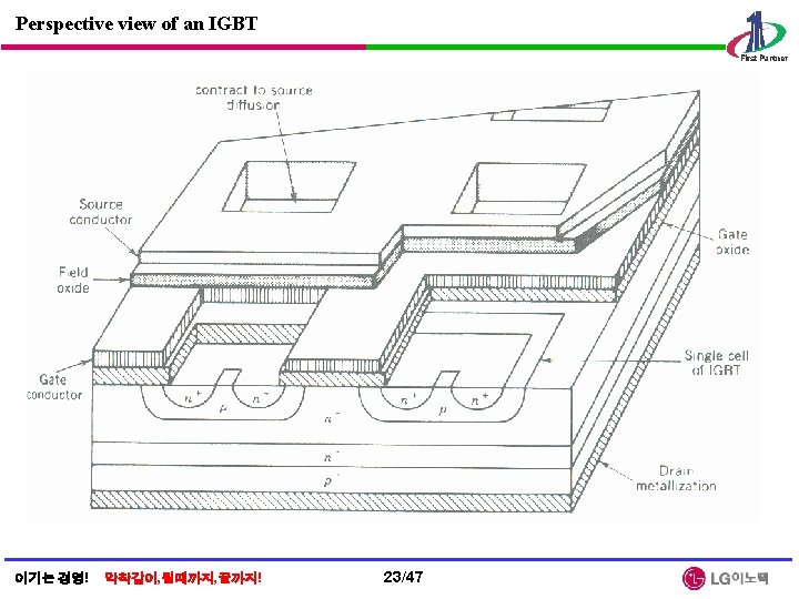
Vertical cross section of an IGBT • Cell structure similar to power MOSFET (VDMOS) cell. • P-region at collector end unique feature of IGBT compared to MOSFET. • Punch-through (PT) IGBT - N+ buffer layer present. • Junction labled J 1 is the reverse-blocking junction • Junction labled J 2 is the forward-blocking junction 이기는 경영! 악착같이, 될때까지, 끝까지! 24/47
The IGBT current-voltage charactoristics Device Symbol • The characteristics of an n-channel IGBT apears similar to those of a logic-level BJT. 이기는 경영! 악착같이, 될때까지, 끝까지! 25/47
On-state Operation 1. The gate drive circuit controls directly the MOSFET channel of the IGBT and, through the drain current of the MOSFET, the base current of its bipolar portion. 2. By its MOSFET portion, the turn-on losses will be significantly affected by the gate drive impedance. Notice the turn-off delay of the current waveform during the Miller effect. The on-state current flow paths 3. An increase in gate drive impedance prolongs the Miller effect and causes a delay in the current fall time that is similar to a storage time. 4. The impact of the gate drive impedance on total switching losses depends on the basic design of the IGBT and its speed. 5. The faster the IGBT the greater its sensitivity to the gate drive impedance. 이기는 경영! 악착같이, 될때까지, 끝까지! 26/47
Equivalent circuit for the IGBT The effective MOSFET and BJT operating portions of the structure Equivalent circuit showing the transistors comprising the parasitic thyristor Approximate equivalent circuit Forward-bias voltage drop across pn junction = 0. 7 V 이기는 경영! 악착같이, 될때까지, 끝까지! 27/47
Switching caracteristics –Turn-on Transient 1. The Turn-on portions of the waveforms appear similar to those of the power MOSFET 2. The gate-drain capacitance Cgd will increase in the MOSFET portion of the IGBT at low drain-source voltage in a manner similar to that observed with power MOSFETs. 3. The pnp transistor portion of IGBT traveses the active region to its on state more slowly than the MOSFET portion of the IGBT. Until the pnp transistor is full on, the full benefit of conductivity modulation of the drain-drift region has not been achieved. 이기는 경영! 악착같이, 될때까지, 끝까지! 28/47
Switching caracteristics –Turn-off Transient Tailing current 이기는 경영! 악착같이, 될때까지, 끝까지! 29/47 1. Major different : 2. Turn-off is observed in the drain current waveform where there are two dstinct time intervals. 3. The “tailing” of the drain current during the second interval tfi 2 is due to the stored charge in the n- drift region. 2. The “tailing” of the drain current 3. Punch-through IGBTs attempt to minimize the current tailing problem by shortening the duration of the tailing time.
Fast recovery diode Outline • Basic structure and I-V characteristics • Switching waveforms • Reverse recovery 이기는 경영! 악착같이, 될때까지, 끝까지! 30/47
Basic structure and I-V characteristics 1. The reverse bias portion of the characteristic shows avalanche breakdown at BVBD. 2. The exponential i-v relationship in forward bias expected from signal-level diode. 3. Characteristics is masked by the ohmic resistance RON in power diode. 이기는 경영! 악착같이, 될때까지, 끝까지! 31/47 1. The n- layer , which is often termed the drift region, is the prime structural feature not found in low-power diodes. 2. The drift region establishes what the reverse breakdown voltage will be.
Switching waveforms trr tfr 이기는 경영! 악착같이, 될때까지, 끝까지! 32/47 1. A power diode requires a finite time to switch from the blocking state (reverse bias) to the on state (forward bias). 2. Both the transition times and the shapes of the waveforms are affected by the intrinsic properties of the diode and by the circuit in which the diode is embedded. 3. The power diodes are very often used in circuits containing inductances that control the rate of change of current, or the diodes are used as freewheeling diodes where the turn-off of a solid-state device controls di/dt.
HV Floating MOS-Gate Driver ICs Outline • Gate drive requirements of high side devices • Block diagram of a typical MGD (MOSFET Gate Drive) • Bootstrap operation • How to select the bootstrap components • The power dissipation in the MGD 이기는 경영! 악착같이, 될때까지, 끝까지! 33/47
1. Gate Drive Requirements Of High-Side Devices 이기는 경영! 악착같이, 될때까지, 끝까지! 1. Gate voltage must be 10 -15 V higher than the drain voltage. Being a high side switch, such gate voltage would have to be higher than the rail voltage, which is frequently the highest voltage available in the system. 2. The gate voltage must be controllable from the logic, which is normally referenced to ground. Thus, the control signals have to be level-shifted to the source of the high side power device, which, in most applications, swings between the two rails. 3. The power absorbed by the gate drive circuitry should not significantly affect the overall efficiency. 34/47
1 -1. Gate Drive Method Of High-Side Devices 이기는 경영! 악착같이, 될때까지, 끝까지! 35/47
2. A Typical Block Diagram VDD/ VBS LEVEL TRANSLATOR 2. 1. Input logic § Controlled by TTL/CMOS compatible inputs. § Schmitt trigger buffers with hysteresis equal to 10% of VDD to accept inputs with long rise time. § Application that require a minimum deadtime should use MGDs with independent drive and relay on a few passive components to build a deadtime. § The propagation delay between input command gate drive output is approximately the same for both channels at turn-on (120 ns) as well as turn-off (95 ns) with a temperature dependence characterized. § The signals from the input logic are coupled to the individual channels. This allows the ground reference of the logic supply (VSS on pin 13) to swing by ± 5 V with respect to the power ground (COM). 이기는 경영! 악착같이, 될때까지, 끝까지! 36/47
2. 2. Low Side Channel § The output stage is implemented either with two N-Channel MOSFETs or with an N-Channel and a PChannel CMOS inverter stage. § Each MOSFET can sink or source-gate currents from 0. 12 to 2 A, depending on the MGD. § The source of the lower driver is independently brought out to pin 2 so that a direct connection can be made to the source of the power device for the return of the gate drive current. 2. 3. High Side Channel § This channel has been built into an “isolation tub” capable of floating from 500 or 600 V to -5 V with respect to power ground (COM). § The gate charge for the high side MOSFET is provided by the bootstrap capacitor which is charged by the 15 V supply through the bootstrap diode during the time when the device is off. 이기는 경영! 악착같이, 될때까지, 끝까지! 37/47
3. How To Select The Bootstrap Components Qg = Gate charge of high side FET f = frequency of operation Icbs(leak) = Bootstrap capacitor leakage current Ilson = 20 m. A, Ilsoff =20 m. A, tw=200 ns Vf = Forward voltage drop across the bootstrap diode VLS = Voltage drop across the low side FET or load Qls = level shift charge required per cycle = 5 n. C (500 V/600 V IC’s) or 20 n. C (1200 V IC’s) • The bootstrap diode must be able to block the full voltage seen in the specific circuit → This occurs when the top device is on and is about equal to the voltage across the power rail. • The high temperature reverse leakage characteristic of this diode can be an important parameter in those applications where the capacitor has to hold the charge for a prolonged period of time. • For the same reason it is important that this diode be ultrafast recovery to reduce the amount of charge that is fed back from the bootstrap capacitor into the supply. 이기는 경영! 악착같이, 될때까지, 끝까지! 38/47
If the capacitor is too large, time is wasted charging the capacitor, with the result being a limit on the maximum duty cycle and PWM frequency. If the capacitor is too small, the voltage drop can be too large at the time the charge is transferred from the CBOOT to the MOSFET gate. To keep the voltage drop small: QBOOT >> QGATE where a factor in the range of 10 to 20 is reasonable. Using 20 as the factor: QBOOT = CBOOT × VBOOT = QGATE × 20 And CBOOT = QGATE × 20 / VBOOT The voltage drop on the BOOT pin, as the MOSFET is being turned on, can be approximated by: Delta_V = QGATE / CBOOT 이기는 경영! 악착같이, 될때까지, 끝까지! 39/47
4. The Power Dissipation In An MGD a) Low voltage static losses are due to the quiescent currents from the three low voltage supplies V DD, VCC and VSS. In a typical 15 V application these losses amount to approximately 3. 5 m. W at 25°C, going to 5 m. W at TJ = 125 °C. b) Low voltage dynamic losses on the VCC supply are due to two different components: b 1) Whenever a capacitor is charged or discharged through a resistor, half of energy that goes into the capacitance is dissipated in the resistor. Thus, the losses in the gate drive resistance, internal and external to the MGD. b 2)Dynamic losses associated with the switching of the internal CMOS circuitry. c) High voltage static losses are mainly due to the leakage currents in the level shifting stage. They are dependent on the voltage applied on the VS pin and they are proportional to the duty cycle, since they only occur when the high side power device is on. d) High voltage switching losses (PD(hv)sw) comprise two terms, one due to the level shifting circuit and one due to the charging and discharging of the capacitance of the high side p-well. d 1) Whenever the high side flip-flop is reset, a command to turn-off the high side device (i. e. , to set the flip-flop) causes a current to flow through the level-shifting circuit. d 2) In a high-side/low-side power circuit the well capacitance Cb-sub is charged and discharged every time VS swings between VR and COM. 이기는 경영! 악착같이, 될때까지, 끝까지! 40/47
5. How To Deal With Negative Transients On The VS PIN Of the problems caused by parasitics, one of the main issues for control ICs is a tendency for the VS node to undershoot ground following switching events. Improve local decoupling a. Increase the bootstrap capacitor (Cb) value to above 0. 47 m. F using at least one low-ESR capacitor. This will reduce overcharging from severe Vs undershoot. b. Use a second low-ESR capacitor from Vcc to COM. As this capacitor supports both the low-side output buffer and bootstrap recharge, we recommend a value at least ten times higher than Cb. c. If a resistor is needed in series with the bootstrap diode, verify that VB does not fall below COM, especially during start-up and extremes of frequency and duty cycle. Look at the Vs spike during the reverse recovery Reduce control IC exposure a. Minimize parasitics in the gate drive circuit by using short, direct tracks. b. Locate the control IC as close as possible to the power switches. 이기는 경영! 악착같이, 될때까지, 끝까지! 41/47
Power MOSFET Datasheet Part Number Main Features Intended application Schematic Package Style 이기는 경영! 악착같이, 될때까지, 끝까지! 42/47
Electrical Characteristics Breakdown Voltage Off-state Leakage current Gate Leakage current VGS Cgd +Cgs gm Cgd 이기는 경영! 악착같이, 될때까지, 끝까지! 43/47 RDS, on Cgd +Cds
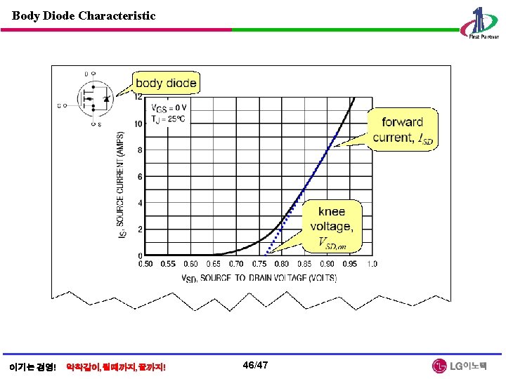
Switching Characteristics switching speed in ns range on-voltage of the body diode Reverse recovery time of the body diode 이기는 경영! 악착같이, 될때까지, 끝까지! 44/47
Electrical Characteristic slope = 1/RDS, on slope = 1/RDS saturation characteristics not important unless for amplification RDS, on decreases with increases in VGS 이기는 경영! 악착같이, 될때까지, 끝까지! RDS, on increases with temperature 45/47
Safe Operating Area (SOA) maximum IDS allowed by metal connections Current limited by RDS, on thermal limit (max power dissipation) Operation must be inside this area limited by breakdown voltage 이기는 경영! 악착같이, 될때까지, 끝까지! 47/47