SemiClassical Transport Theory Outline l What is Computational


 2. Alternative")


![MOTIVATION 150 Width [nm] 140 130 120 110 100 60 80 100 120 140](https://slidetodoc.com/presentation_image/261ee6dd0520a927918b6717af232bf7/image-52.jpg "MOTIVATION 150 Width [nm] 140 130 120 110 100 60 80 100 120 140")
 Corrected Coulomb Approach and Discrete/Unintentional (2)")


 Stolk et al. result: (100% of the fluctuations)")
![MOSFETs - Discrete Impurity Effects Approach 1 [1]: Approach 2 [2]: [1] T. Mizuno,](https://slidetodoc.com/presentation_image/261ee6dd0520a927918b6717af232bf7/image-60.jpg "MOSFETs - Discrete Impurity Effects Approach 1 [1]: Approach 2 [2]: [1] T. Mizuno,")


: S. S. Ahmed and D.")


- Slides: 73
Semi-Classical Transport Theory
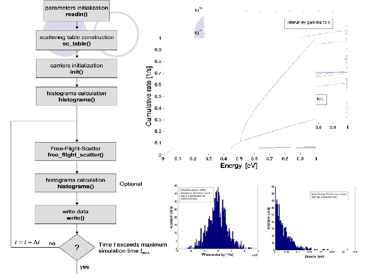
Outline: l What is Computational Electronics? l Semi-Classical Transport Theory ¡ Drift-Diffusion Simulations ¡ Hydrodynamic Simulations ¡ Particle-Based Device Simulations l Inclusion of Tunneling and Size-Quantization Effects in Semi-Classical Simulators ¡ Tunneling Effect: WKB Approximation and Transfer Matrix Approach ¡ Quantum-Mechanical Size Quantization Effect l Drift-Diffusion and Hydrodynamics: Quantum Correction and Quantum Moment Methods l Particle-Based Device Simulations: Effective Potential Approach l Quantum Transport ¡ Direct Solution of the Schrodinger Equation (Usuki Method) and Theoretical Basis of the Green’s Functions Approach (NEGF) ¡ NEGF: Recursive Green’s Function Technique and CBR Approach ¡ Atomistic Simulations – The Future l Prologue
Direct Solution of the Boltzmann Transport Equation Particle-Based Approaches ¡ Spherical Harmonics ¡ Numerical Solution of the Boltzmann-Poisson Problem ¡ l In here we will focus on Particle-Based (Monte Carlo) approaches to solving the Boltzmann Transport Equation
Ways of Solving the BTE Using MCT l Single particle Monte Carlo Technique ¡ Follow single particle for long enough time to collect sufficient statistics ¡ Practical for characterization of bulk materials or inversion layers l Ensemble Monte Carlo Technique ¡ MUST BE USED when modeling SEMICONDUCTOR DEVICES to have the complete self-consistency built in Carlo Jacoboni and Lino Reggiani, The Monte Carlo method for the solution of charge transport in semiconductors with applications to covalent materials, Rev. Mod. Phys. 55, 645 - 705 (1983).
Path-Integral Solution to the BTE l The path integral solution of the Boltzmann Transport Equation (BTE), where L=N t and tn=n t, is of the form: K. K. Thornber and Richard P. Feynman, Phys. Rev. B 1, 4099 (1970).
l The two-step procedure is then found by using N=1, which means that t= t, i. e. : Intermediate function that describes the occupancy of the state (p+e. E t) at time t=0, which can be changed due to scattering events (SCATTER) + Integration over a trajectory, i. e. probability that no scattering occurred within time integral t (FREE FLIGHT)
Monte Carlo Approach to Solving the Boltzmann Transport Equation l Using path integral formulation to the BTE one can show that one can decompose the solution procedure into two components: 1. 2. Carrier free-flights that are interrupted by scattering events Memory-less scattering events that change the momentum and the energy of the particle instantaneously
Particle Trajectories in Phase Space
Carrier Free-Flights q The probability of an electron scattering in a small time interval dt is (k)dt, where (k) is the total transition rate per unit time. Time dependence originates from the change in k(t) during acceleration by external forces where v is the velocity of the particle. q The probability that an electron has not scattered after scattering at t = 0 is: q It is this (unnormalized) probability that we utilize as a non-uniform distribution of free flight times over a semi-infinite interval 0 to . We want to sample random flight times from this non-uniform distribution using uniformly distributed random numbers over the interval 0 to 1.
Generation of Random Flight Times Hence, we choose a random number Ith particle first random number We have a problem with this integral! We solve this by introducing a new, fictitious scattering process which does not change energy or momentum:
Generation of Random Flight Times The sum runs over all the real scattering processes. To this we add the fictitious self-scattering which is chosen to have a nice property:
Self-Scattering
Self-Scattering
Free-Flight Scatter Sequence for Ensemble Monte Carlo Particle time scale However, we need a second time scale, which provides the times at which the ensemble is “stopped” and averages are computed. = collisions
Free-Flight Scatter Sequence R. W. Hockney and J. W. Eastwood, Computer Simulation Using Particles, 1983.
Choice of Scattering Event Terminating Free Flight o At the end of the free flight ti, the type of scattering which ends the flight (either real or self-scattering) must be chosen according to the relative probabilities for each mechanism. o Assume that the total scattering rate for each scattering mechanism is a function only of the energy, E, of the particle at the end of the free flight where the rates due to the real scattering mechanisms are typically stored in a lookup table. o A histogram is formed of the scattering rates, and a random number r is used as a pointer to select the right mechanism. This is schematically shown on the next slide.
Choice of Scattering Event Terminating Free-Flight We can make a table of the scattering processes at the energy of the particle at the scattering time: Selection process for scattering
Look-up table of scattering rates: Store the total scattering rates in a table for a grid in energy ………
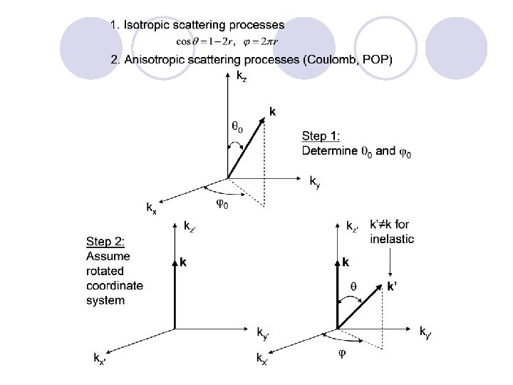
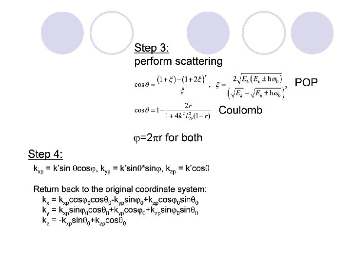
Choice of the Final State After Scattering l Using a random number and probability distribution function l Using analytical expressions (slides that follow)
Representative Simulation Results From Bulk Simulations - Ga. As Simulation Results Obtained by D. Vasileska’s Monte Carlo Code.
Transient Data
Steady-State Results Gunn Effect
Particle-Based Device Simulations l In a particle-based device simulation approach the Poisson equation is decoupled from the BTE over a short time period dt smaller than the dielectric relaxation time ¡ Poisson and BTE are solved in a time-marching manner ¡ During each time step dt the electric field is assumed to be constant (kept frozen)
Particle-Mesh Coupling The particle-mesh coupling scheme consists of the following steps: - Assign charge to the Poisson solver mesh - Solve Poisson’s equation for V(r) - Calculate the force and interpolate it to the particle locations - Solve the equations of motion: Laux, S. E. , On particle-mesh coupling in Monte Carlo semiconductor device simulation, Computer-Aided Design of Integrated Circuits and Systems, IEEE Transactions on, Volume 15, Issue 10, Oct 1996 Page(s): 1266 - 1277
Assign Charge to the Poisson Mesh 1. Nearest grid point scheme 2. Nearest element cell scheme 3. Cloud in cell scheme
Force interpolation l The SAME METHOD that is used for the charge assignment has to be used for the FORCE INTERPOLATION: xp-1 xp xp+1
Treatment of the Contacts From the aspect of device physics, one can distinguish between the following types of contacts: (1) Contacts, which allow a current flow in and out of the device - Ohmic contacts: purely voltage or purely current controlled - Schottky contacts (2) Contacts where only voltages can be applied
Calculation of the Current l The current in steady-state conditions is calculated in two ways: By counting the total number of particles that enter/exit particular contact ¡ By using the Ramo-Shockley theorem according to which, in the channel, the current is calculated using ¡
Current Calculated by Counting the Net Number of Particles Exiting/Entering a Contact
Device Simulation Results for MOSFETs: Current Conservation VG=1. 4 V, VD=1 V Drain contact Source contact Cumulative net number of particles Entering/exiting a contact for a 50 nm Channel length device X. He, MS, ASU, 2000. Current calculated using Ramo-Schockley formula
Simulation Results for MOSFETs: Velocity and Enery Along the Channel Velocity overshoot effect observed throughout the whole channel length of the device – non-stationary transport. For the bias conditions used average electron energy is smaller that 0. 6 e. V which justifies the use of non-parabolic band model.
Simulation Results for MOSFETs: IV Characteristics The differences between the Monte Carlo and the Silvaco simulations are due to the following reasons: • Different transport models used (nonstationary transport is taking place in this device structure). • Surface-roughness and Coulomb scattering are not included in theoretical model used in the 2 D-MCPS. X. He, MS, ASU, 2000.
Simulation Results For SOI MESFET Devices – Where are the Carriers? SOI MOSFET SOI MESFET Applications: Micropower circuits based on weakly inverted MOSFETs Digital Watch Pacemaker Implantable cochlea and retina Low-power RF electronics. T. J. Thornton, IEEE Electron Dev. Lett. , 8171 (1985).
Proper Modeling of SOI MESFET Device Gate current calculation: l WKB Approximation l Transfer Matrix Approach for piece-wise linear potentials Interface-Roughness: l K-space treatment l Real-space treatment Goodnick et al. , Phys. Rev. B 32, 8171 (1985)
Output Characteristics and Cut-off Frequency of a Si MESFET Device Tarik Khan, Ph. D, ASU, 2004.
Output Characteristics and Cut-off Frequency of a Si MESFET Device Tarik Khan, Ph. D, ASU, 2004.
Modeling of SOI Devices l When modeling SOI devices lattice heating effects has to be accounted for l In what follows we discuss the following: Comparison of the Monte Carlo, Hydrodynamic and Drift-Diffusion results of Fully-Depleted SOI Device Structures* ¡ Impact of self-heating effects on the operation of the same generations of Fully-Depleted SOI Devices ¡ *D. Vasileska. K. Raleva and S. M. Goodnick, IEEE Trans. Electron Dev. , in press.
FD-SOI Devices: Monte Carlo vs. Hydrodynamic vs. Drift-Diffusion 90 nm Silvaco ATLAS simulations performed by Prof. Vasileska.
FD-SOI Devices: Monte Carlo vs. Hydrodynamic vs. Drift-Diffusion 25 nm Silvaco ATLAS simulations performed by Prof. Vasileska.
FD-SOI Devices: Monte Carlo vs. Hydrodynamic vs. Drift-Diffusion 14 nm Silvaco ATLAS simulations performed by Prof. Vasileska.
FD-SOI Devices: Why Self-Heating Effect is Important? 1. Alternative materials (Si. Ge) 2. Alternative device designs (FD SOI, DG, TG, MG, Fin-FET transistors
FD-SOI Devices: Why Self-Heating Effect is Important? L~ 300 nm d. S A. Majumdar, “Microscale Heat Conduction in Dielectric Thin Films, ” Journal of Heat Transfer, Vol. 115, pp. 7 -16, 1993.
Conductivity of Thin Silicon Films – Vasileska Empirical Formula
Particle-Based Device Simulator That Includes Heating
Heating vs. Different Technology Generation
Higher Order Effects Inclusion in Particle. Based Simulators l Degeneracy – Pauli Exclusion Principle l Short-Range Coulomb Interactions ¡ Fast Multipole Method (FMM) V. Rokhlin and L. Greengard, J. Comp. Phys. , 73, pp. 325 -348 (1987). ¡ Corrected Coulomb Approach W. J. Gross, D. Vasileska and D. K. Ferry, IEEE Electron Device Lett. 20, No. 9, pp. 463 -465 (1999). ¡ P 3 M Method Hockney and Eastwood, Computer Simulation Using Particles.
MOTIVATION Potential, Courtesy of Dragica Vasileska, 3 D-DD Simulation, 1994.
MOTIVATION 150 Width [nm] 140 130 120 110 100 60 80 100 120 140 Length [nm] Current Stream Lines, Courtesy of Dragica Vasileska, 3 D-DD Simulation, 1994.
The ASU Particle-Based Device Simulator Short-Range Interactions (1) Corrected Coulomb Approach and Discrete/Unintentional (2) P 3 M Algorithm Dopants (3) Fast Multipole Method (FMM) Long-range Interactions (3 D Poisson Equation Solver) Quantum Mechanical Size-quantization Effects (1) Ferry’s Effective Potential Method (2) Quantum Field Approach Boltzmann Transport Equations (Particle-Based Monte Carlo Transport Kernel) Statistical Enhancement: Event Biasing Scheme
Significant Data Obtained Between 1998 and 2002
MOSFETs - Standard Characteristics è The average energy of the carriers increases when going from the source to the drain end of the channel. Most of the phonon scattering events occur at the first half of the channel. è Velocity overshoot occurs near the drain end of the channel. The sharp velocity drop is due to e-e and e-i interactions coming from the drain. W. J. Gross, D. Vasileska and D. K. Ferry, "3 D Simulations of Ultra-Small MOSFETs with Real-Space Treatment of the Electron-Electron and Electron-Ion Interactions, " VLSI Design, Vol. 10, pp. 437 -452
MOSFETs - Role of the E-E and E-I source Individual electron trajectories over time channel drain mesh force only with e-e and e-i
MOSFETs - Role of the E-E and E-I Mesh force only With e-e and e-i Short-range e-e and e-i interactions push some of the electrons towards higher energies D. Vasileska, W. J. Gross, and D. K. Ferry, "Monte-Carlo particle-based simulations of deep-submicron n. MOSFETs with real-space treatment of electron-electron and electron-impurity interactions, " Superlattices and Microstructures, Vol. 27, No. 2/3, pp. 147 -157 (2000).
Degradation of Output Characteristics ¤ The short range e -e and e -i interactions have significant influence on the device output characteristics. ¤ There is almost a factor of two decrease in current when these two interaction terms are considered. LG = 35 nm, WG = 35 nm, NA = 5 x 1018 cm-3, Tox = 2 nm, VG = 1 1. 6 V (0. 2 V) LG = 50 nm, WG = 35 nm, NA = 5 x 1018 cm-3 Tox = 2 nm, VG = 1 1. 6 V (0. 2 V) W. J. Gross, D. Vasileska and D. K. Ferry, "Ultra-small MOSFETs: The importance of the full Coulomb interaction on device characteristics, " IEEE Trans. Electron Devices, Vol. 47, No. 10, pp. 1831 -1837 (2000).
Mizuno result: (60% of the fluctuations) Stolk et al. result: (100% of the fluctuations) Depth. Distribution of the charges Fluctuations in the surface potential Fluctuations in the electric field
MOSFETs - Discrete Impurity Effects Approach 1 [1]: Approach 2 [2]: [1] T. Mizuno, J. Okamura, and A. Toriumi, IEEE Trans. Electron Dev. 41, 2216 (1994). [2] P. A. Stolk, F. P. Widdershoven, and D. B. Klaassen, IEEE Trans. Electron Dev. 45, 1960 (1998).
¤ To understand the role that the position of the impurity atoms plays on the threshold voltage fluctuations, statistical ensembles of 5 devices from the low-end, center and the high-end of the distribution were considered. Number of atoms in the channel VT correlation Number of devices ¤ Significant correlation was observed between the threshold voltage and the number of atoms that fall within the first 15 nm depth of the channel. T Threshold voltage [V] Depth Correlation of s. V Number of atoms in the channel Depth [nm]
¤ Impurity distribution in the channel also affects the carrier mobility and saturation current of the device. ¤ Significant correlation was observed between the drift velocity (saturation current) and the number of atoms that fall within the first 10 nm depth of the channel. Drain current [m. A] Fluctuations in High-Field Characteristics VG = 1. 5 V, VD = 1 V Correlation Drift velocity [cm/s] Number of atoms in the channel Depth [nm]
Current Issues in Novel Devices – Unintentional Dopants
THE EXPERIMENT …
Results for SOI Device Size Quantization Effect (Effective Potential): S. S. Ahmed and D. Vasileska, “Threshold voltage shifts in narrow-width SOI devices due to quantum mechanical size-quantization effect”, Physica E, Vol. 19, pp. 48 -52 (2003).
Results for SOI Device Due to the unintentional dopant both the electrostatics and the transport are affected.
Results for SOI Device Unintentional Dopant: D. Vasileska and S. S. Ahmed, “Narrow-Width SOI Devices: The Role of Quantum Mechanical Size Quantization Effect and the Unintentional Doping on the Device Operation”, IEEE Transactions on Electron Devices, Volume 52, Issue 2, Feb. 2005 Page(s): 227 – 236.
Results for SOI Device Channel Width = 10 nm VG = 1. 0 V VD = 0. 1 V
Results for SOI Device Channel Width = 5 nm VG = 1. 0 V VD = 0. 1 V
Results for SOI Device Impurity located at the very source-end, due to the availability of Increasing number of electrons screening the impurity ion, has reduced impact on the overall drain current.
Results for SOI Device D. Vasileska and S. S. Ahmed, IEEE Transactions on Electron Devices, Volume 52, Issue 2, Feb. 2005 Page(s): 227 – 236. S. Ahmed, C. Ringhofer and D. Vasileska, Nanotechnology, IEEE Transactions on, Volume 4, Issue 4, July 2005 Page(s): 465 – 471. D. Vasileska, H. R. Khan and S. S. Ahmed, International Journal of Nanoscience, Invited Review Paper, 2005.
Results for SOI Device Electron-Electron Interactions: D. Vasileska and S. S. Ahmed, IEEE Transactions on Electron Devices, Volume 52, Issue 2, Feb. 2005 Page(s): 227 – 236. S. Ahmed, C. Ringhofer and D. Vasileska, Nanotechnology, IEEE Transactions on, Volume 4, Issue 4, July 2005 Page(s): 465 – 471. D. Vasileska, H. R. Khan and S. S. Ahmed, International Journal of Nanoscience, Invited Review Paper, 2005.
Summary Particle-based device simulations are the most desired tool when modeling transport in devices in which velocity overshoot (non-stationary transport) exists l Particle-based device simulators are rather suitable for modeling ballistic transport in nano-devices l It is rather easy to include short-range electron-electron and electron-ion interactions in particle-based device simulators via a real-space molecular dynamics routine l Quantum-mechanical effects (size quantization and density of states modifications) can be incorporated in the model quite easily with the assumption of adiabatic approximation and solution of the 1 D or 2 D Schrodinger equation in slices along the channel section of the device l