Selex ES Detector Developments Peter Knowles SDW 2013


- Slides: 30

Selex ES Detector Developments Peter Knowles SDW 2013

Established Array Capability • ACRT growth for photoconductors, visible to 20µm • LPE growth on CZT for homojunctions and APDs, visible to 10µm • MOVPE growth on 3” Ga. As substrates for heterostructures, 2 to 14µm • Dual band arrays • Die and wafer scale processing of FPAs, up to 1080 x 1920 • Pixel size down to 12µm

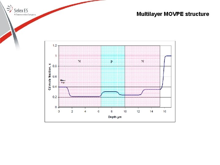
Multilayer MOVPE structure

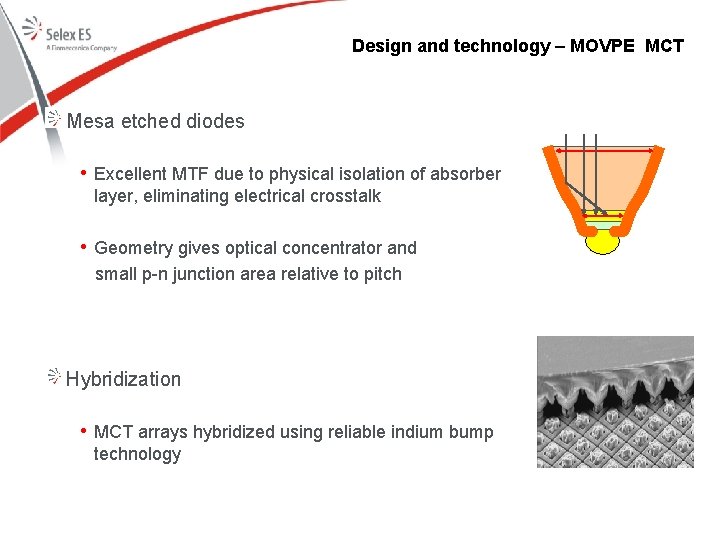
Design and technology – MOVPE MCT Mesa etched diodes • Excellent MTF due to physical isolation of absorber layer, eliminating electrical crosstalk • Geometry gives optical concentrator and small p-n junction area relative to pitch Hybridization • MCT arrays hybridized using reliable indium bump technology

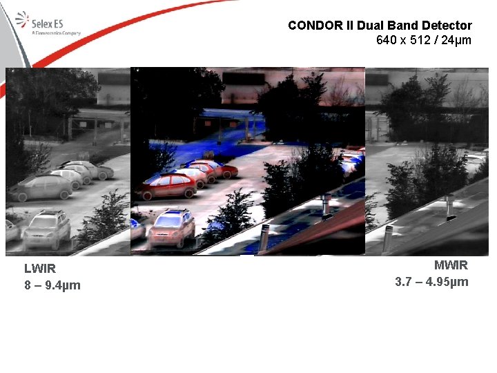
CONDOR II Dual Band Detector 640 x 512 / 24µm DWIR LWIR 8 – 9. 4µm MWIR 3. 7 – 4. 95µm

Complementary Capabilities • In-house ROIC design, 0. 6µm and 0. 35µm CMOS migrating to 0. 18µm • Vacuum packaging and cryogenics • Warm electronics, module sets, and cameras • Tri Glycine Sulphate

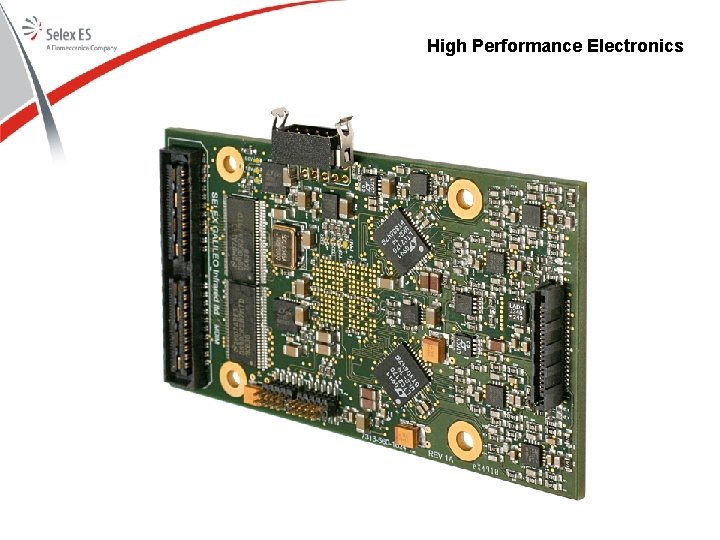
High Performance Electronics

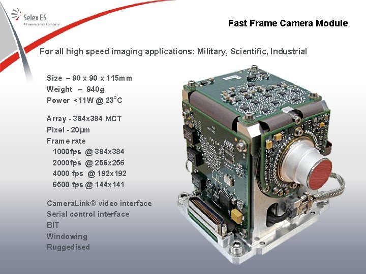
Fast Frame Camera Module For all high speed imaging applications: Military, Scientific, Industrial Size – 90 x 115 mm Weight – 940 g Power <11 W @ 23 o. C Array - 384 x 384 MCT Pixel - 20µm Frame rate 1000 fps @ 384 x 384 2000 fps @ 256 x 256 4000 fps @ 192 x 192 6500 fps @ 144 x 141 Camera. Link® video interface Serial control interface BIT Windowing Ruggedised

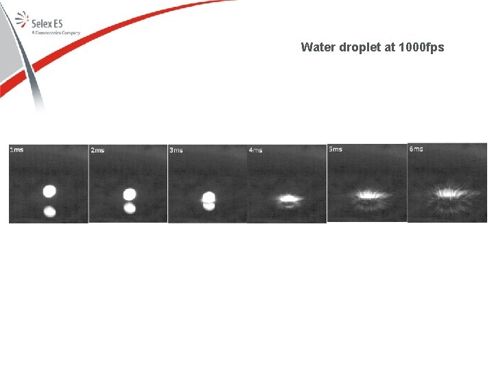
Water droplet at 1000 fps

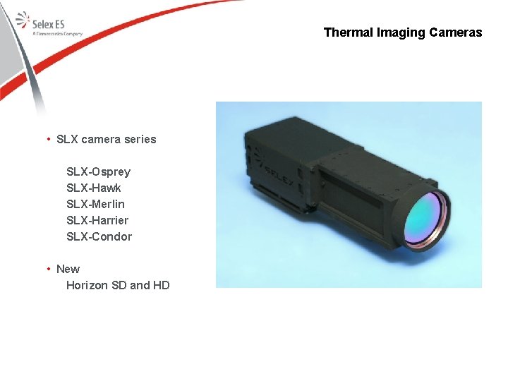
Thermal Imaging Cameras • SLX camera series SLX-Osprey SLX-Hawk SLX-Merlin SLX-Harrier SLX-Condor • New Horizon SD and HD

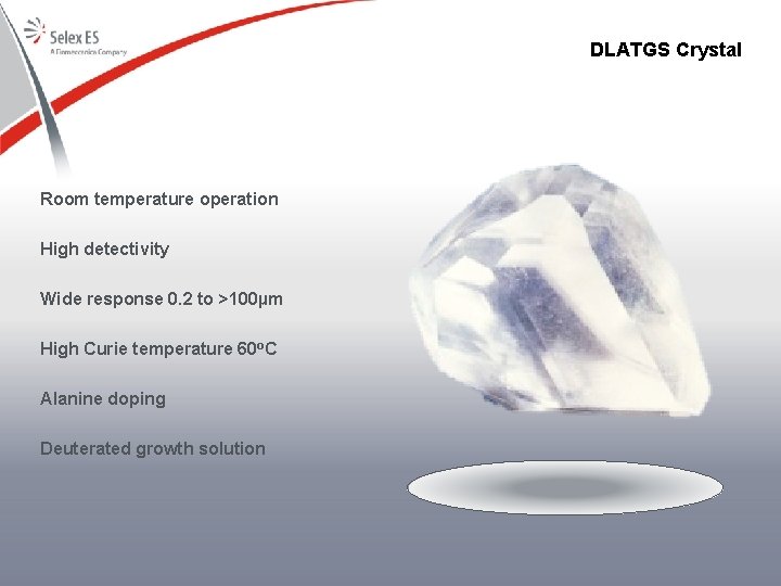
DLATGS Crystal Room temperature operation High detectivity Wide response 0. 2 to >100µm High Curie temperature 60 o. C Alanine doping Deuterated growth solution

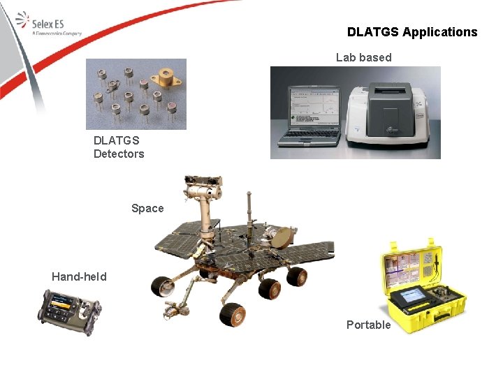
DLATGS Applications Lab based DLATGS Detectors Space Hand-held Portable

Recent Developments HOT Horizon SD and HD cameras Large format ROICs, smaller pixels Space Programmes APDs – LPE and MOVPE Ian Baker and Johann Rothman - Physics and Performance of Hg. Cd. Te APDs Gert Finger – NIR Hg. Cd. Te Avalanche Photodiode Arrays for Wavefront Sensing and Fringe Tracking

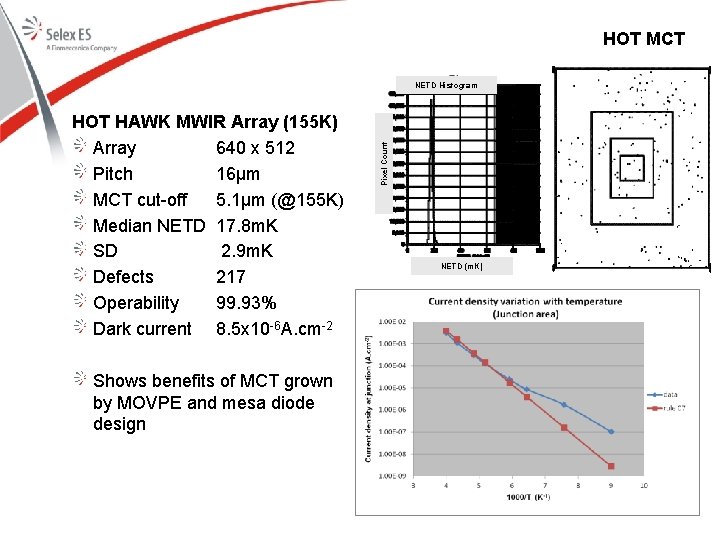
HOT MCT HOT HAWK MWIR Array (155 K) Array 640 x 512 Pitch 16µm MCT cut-off 5. 1µm (@155 K) Median NETD 17. 8 m. K SD 2. 9 m. K Defects 217 Operability 99. 93% Dark current 8. 5 x 10 -6 A. cm-2 Shows benefits of MCT grown by MOVPE and mesa diode design Pixel Count NETD Histogram NETD (m. K)

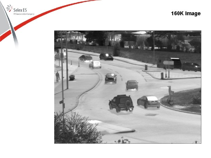
160 K Image

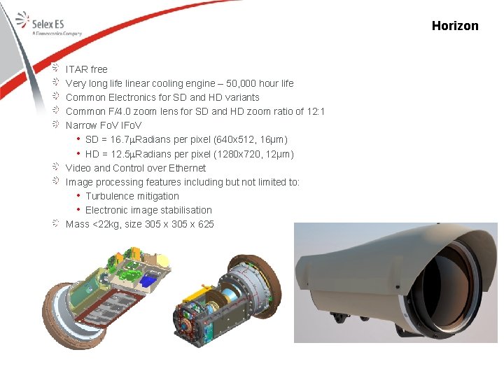
Horizon ITAR free Very long life linear cooling engine – 50, 000 hour life Common Electronics for SD and HD variants Common F/4. 0 zoom lens for SD and HD zoom ratio of 12: 1 Narrow Fo. V IFo. V • SD = 16. 7 Radians per pixel (640 x 512, 16µm) • HD = 12. 5 Radians per pixel (1280 x 720, 12µm) Video and Control over Ethernet Image processing features including but not limited to: • Turbulence mitigation • Electronic image stabilisation Mass <22 kg, size 305 x 625

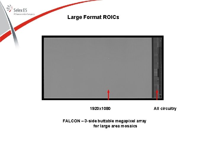
Large Format ROICs 1920 x 1080 FALCON – 3 -side buttable megapixel array for large area mosaics All circuitry

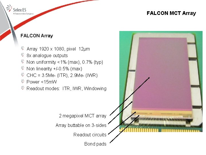
FALCON MCT Array FALCON Array 1920 x 1080, pixel 12µm 8 x analogue outputs Non uniformity <1% (max), 0. 7% (typ) Non linearity +/-0. 5% (max) CHC = 3. 5 Me- (ITR), 2. 9 Me- (IWR) Power <15 m. W Readout modes: ITR, IWR, Windowing 2 megapixel MCT array Array buttable on 3 -sides Readout circuits Bond pads

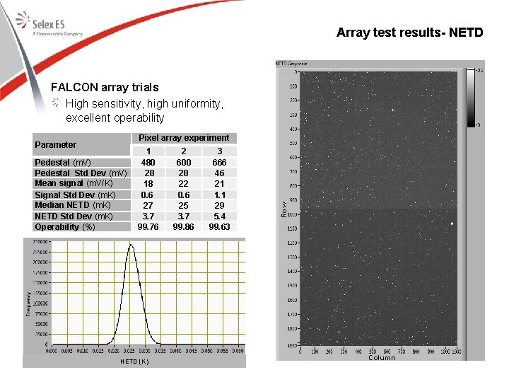
Array test results- NETD FALCON array trials High sensitivity, high uniformity, excellent operability Pedestal (m. V) Pedestal Std Dev (m. V) Mean signal (m. V/K) Signal Std Dev (m. K) Median NETD (m. K) NETD Std Dev (m. K) Operability (%) 1 480 28 18 0. 6 27 3. 7 99. 76 NETD (K) 2 600 28 22 0. 6 25 3. 7 99. 86 3 666 46 21 1. 1 29 5. 4 99. 63 Row Pixel array experiment Parameter Column

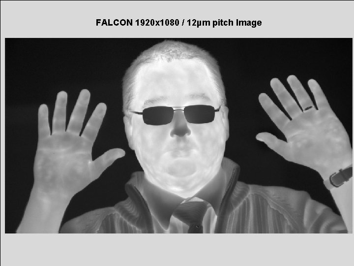
FALCON 1920 x 1080 / 12µm pitch Image

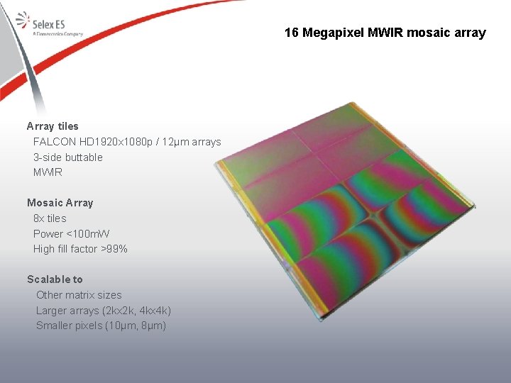
16 Megapixel MWIR mosaic array Array tiles FALCON HD 1920 x 1080 p / 12µm arrays 3 -side buttable MWIR Mosaic Array 8 x tiles Power <100 m. W High fill factor >99% Scalable to Other matrix sizes Larger arrays (2 kx 2 k, 4 kx 4 k) Smaller pixels (10µm, 8µm)

Space Programmes Large format Near Infrared Array (ESA) Currently in phase 2: deliverable is 1032 x 1280, 15 m pitch, 2. 1µm cut-off, thinned MCT Source follower architecture, enabled for APDs Selex provide consultancy and test facility to Caeleste on parallel ASIC development SWIR development (ESA) 2048 x 2048, 17 m pitch, 2. 5 m cut-off, enabled for APDs, thinned MCT VLWIR development (ESA) Low dark current Up to 14. 5 m cut-off wavelength OSIRIS Rex Thermal Emission Spectrometer (Arizona State University) NASA asteroid sample return mission DLATGS uncooled pyroelectric detector 4 – 50 m spectral response

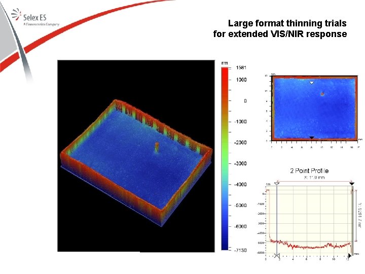
Large format thinning trials for extended VIS/NIR response

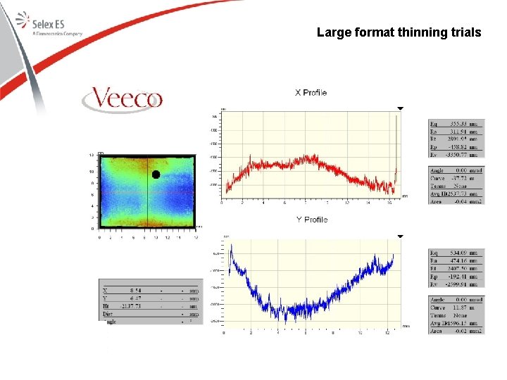
Large format thinning trials

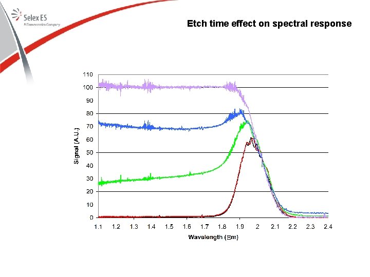
Etch time effect on spectral response

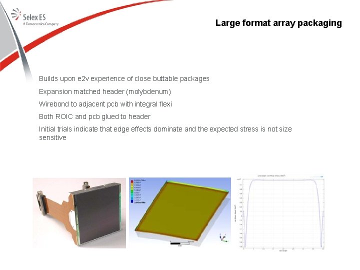
Large format array packaging Builds upon e 2 v experience of close buttable packages Expansion matched header (molybdenum) Wirebond to adjacent pcb with integral flexi Both ROIC and pcb glued to header Initial trials indicate that edge effects dominate and the expected stress is not size sensitive

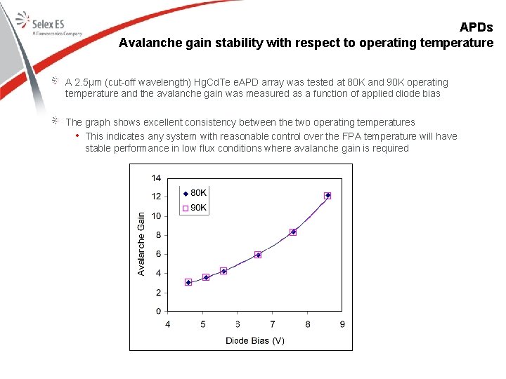
APDs Avalanche gain stability with respect to operating temperature A 2. 5μm (cut-off wavelength) Hg. Cd. Te e. APD array was tested at 80 K and 90 K operating temperature and the avalanche gain was measured as a function of applied diode bias The graph shows excellent consistency between the two operating temperatures • This indicates any system with reasonable control over the FPA temperature will have stable performance in low flux conditions where avalanche gain is required

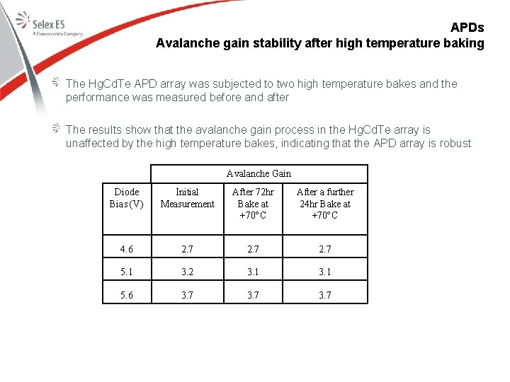
APDs Avalanche gain stability after high temperature baking The Hg. Cd. Te APD array was subjected to two high temperature bakes and the performance was measured before and after The results show that the avalanche gain process in the Hg. Cd. Te array is unaffected by the high temperature bakes, indicating that the APD array is robust Avalanche Gain Diode Bias (V) Initial Measurement After 72 hr Bake at +70 C After a further 24 hr Bake at +70 C 4. 6 2. 7 5. 1 3. 2 3. 1 5. 6 3. 7

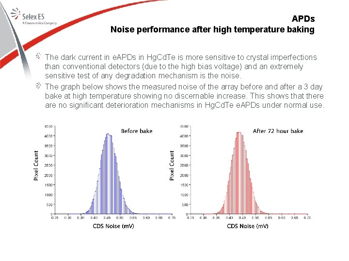
APDs Noise performance after high temperature baking The dark current in e. APDs in Hg. Cd. Te is more sensitive to crystal imperfections than conventional detectors (due to the high bias voltage) and an extremely sensitive test of any degradation mechanism is the noise. The graph below shows the measured noise of the array before and after a 3 day bake at high temperature showing no discernable increase. This shows that there are no significant deterioration mechanisms in Hg. Cd. Te e. APDs under normal use.

FALCON 1920 x 1080 / 12µm pitch Image