Selected Topics on Logic Synthesis and FPGA Design
- Slides: 43

Selected Topics on Logic Synthesis and FPGA Design Andres Cicuttin ICTP-INFN Microprocessor Laboratory Trieste, 2006 Andres Cicuttin, MLab INFN-ICTP

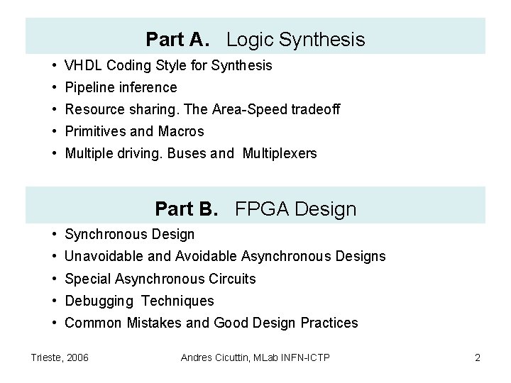
Part A. Logic Synthesis • VHDL Coding Style for Synthesis • Pipeline inference • Resource sharing. The Area-Speed tradeoff • Primitives and Macros • Multiple driving. Buses and Multiplexers Part B. FPGA Design • Synchronous Design • Unavoidable and Avoidable Asynchronous Designs • Special Asynchronous Circuits • Debugging Techniques • Common Mistakes and Good Design Practices Trieste, 2006 Andres Cicuttin, MLab INFN-ICTP 2

Some References • Books on VHDL and FPGA design: – The Design Warrior’s guide to FPGAs, Cleve “Max” Maxfield (Elsevier, 2004) – Digital Signal Processing with Field Programmable Gate Arrays, U. Meyer-Baese (Springer, 2004) – Real Chip Design and Verification, Ben Cohen, (Vhdl. Cohen Publishing, 2002) • Web sites: – – www. opencores. org, http: //asics. ws, www. fpga 4 fun. com, www. us. design-reuse. com, www. fpga-faq. org, http: //www. andraka. com/papers. htm, … Websites of FPGA companies (Actel, Altera, Xilinx, …) Trieste, 2006 Andres Cicuttin, MLab INFN-ICTP 3

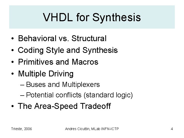
VHDL for Synthesis • • Behavioral vs. Structural Coding Style and Synthesis Primitives and Macros Multiple Driving – Buses and Multiplexers – Potential conflicts (standard logic) • The Area-Speed Tradeoff Trieste, 2006 Andres Cicuttin, MLab INFN-ICTP 4

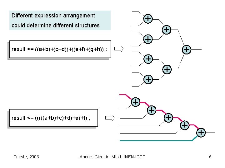
Different expression arrangement could determine different structures result <= ((a+b)+(c+d))+((e+f)+(g+h)) ; result <= (((((a+b)+c)+d)+e)+f) ; Trieste, 2006 Andres Cicuttin, MLab INFN-ICTP 5

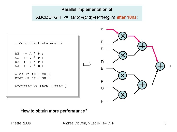
Parallel implementation of ABCDEFGH <= (a*b)+(c*d)+(e*f)+(g*h) after 10 ns; A B --Concurrent statements C AB CD EF GH <= <= A C E G * * B D F H ; ; D E ABCD <= AB + CD ; EFGH <= EF + GH ; F ABCDEFGH <= ABCD + EFGH ; G H How to obtain more performance? Trieste, 2006 Andres Cicuttin, MLab INFN-ICTP 6

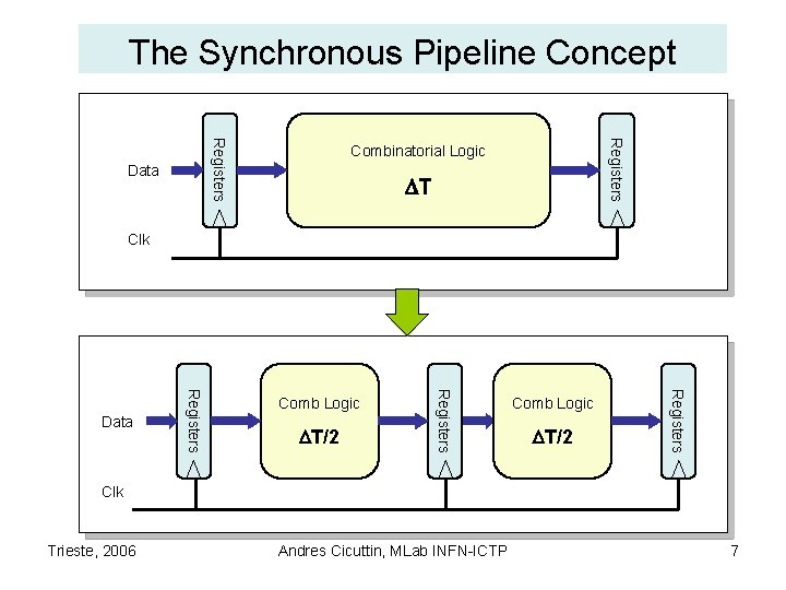
The Synchronous Pipeline Concept Registers Data Combinatorial Logic DT Clk Comb Logic DT/2 Registers Data Comb Logic Clk Trieste, 2006 Andres Cicuttin, MLab INFN-ICTP 7

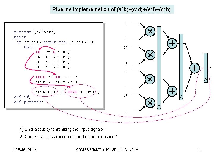
Pipeline implementation of (a*b)+(c*d)+(e*f)+(g*h) A process (<clock>) begin if <clock>'event then AB <= A CD <= C EF <= E GH <= G and <clock>='1' * * B D F H B C ; ; D E ABCD <= AB + CD ; EFGH <= EF + GH ; ABCDEFGH <= ABCD + EFGH ; end if; end process; F G H 1) what about synchronizing the Input signals? 2) Can we use less resources for the same function? Trieste, 2006 Andres Cicuttin, MLab INFN-ICTP 8

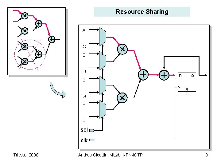
Resource Sharing A C B D E D Q R G F H sel clk Trieste, 2006 Andres Cicuttin, MLab INFN-ICTP 9

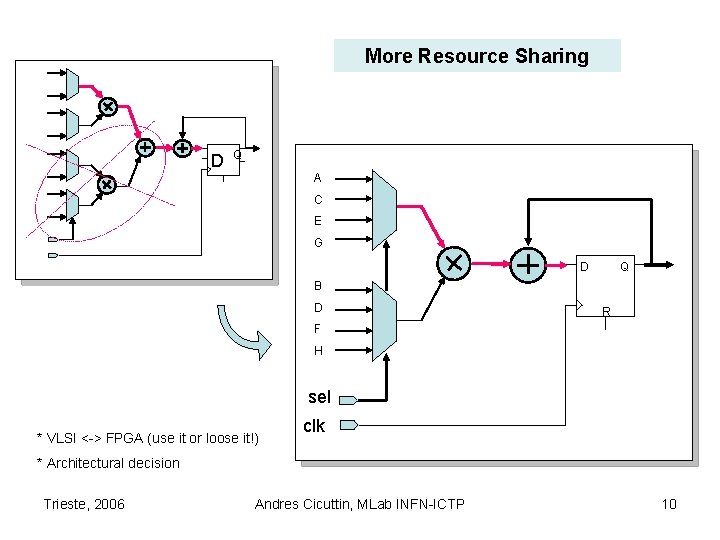
More Resource Sharing D Q A C E G D Q B D R F H sel * VLSI <-> FPGA (use it or loose it!) clk * Architectural decision Trieste, 2006 Andres Cicuttin, MLab INFN-ICTP 10

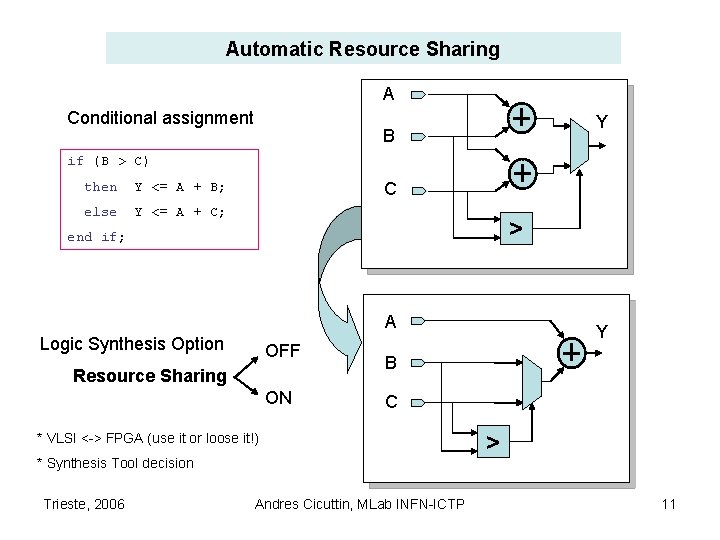
Automatic Resource Sharing A Conditional assignment Y B if (B > C) then Y <= A + B; else Y <= A + C; C > end if; A Logic Synthesis Option OFF Resource Sharing ON B C * VLSI <-> FPGA (use it or loose it!) * Synthesis Tool decision Trieste, 2006 Y Andres Cicuttin, MLab INFN-ICTP > 11

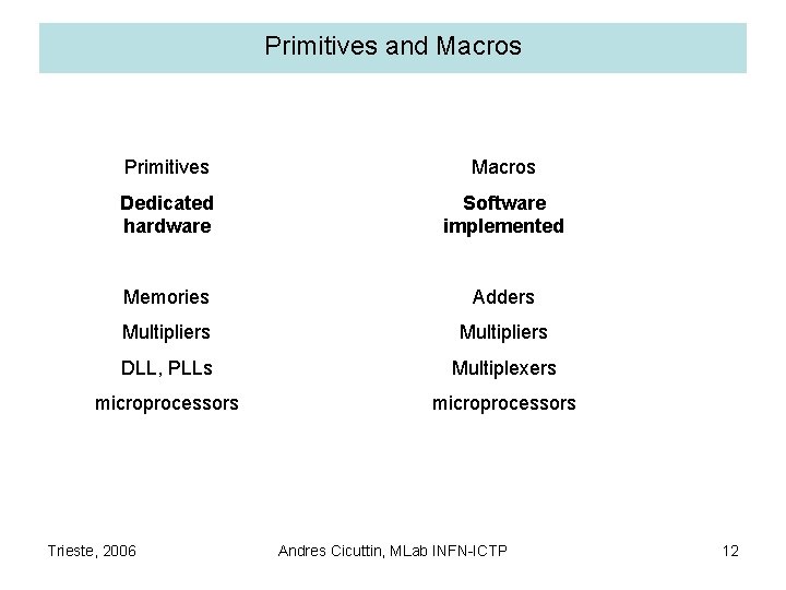
Primitives and Macros Primitives Macros Dedicated hardware Software implemented Memories Adders Multipliers DLL, PLLs Multiplexers microprocessors Trieste, 2006 Andres Cicuttin, MLab INFN-ICTP 12

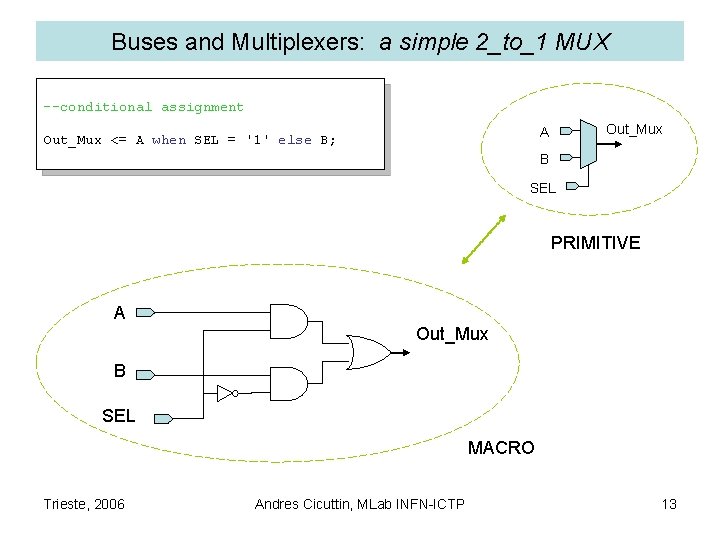
Buses and Multiplexers: a simple 2_to_1 MUX --conditional assignment Out_Mux A Out_Mux <= A when SEL = '1' else B; B SEL PRIMITIVE A Out_Mux B SEL MACRO Trieste, 2006 Andres Cicuttin, MLab INFN-ICTP 13

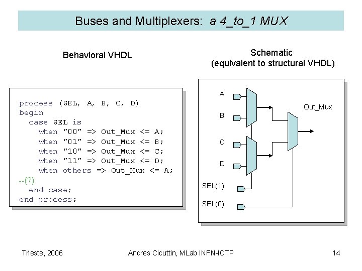
Buses and Multiplexers: a 4_to_1 MUX Behavioral VHDL Schematic (equivalent to structural VHDL) A process (SEL, A, B, C, D) begin case SEL is when "00" => Out_Mux <= A; when "01" => Out_Mux <= B; when "10" => Out_Mux <= C; when "11" => Out_Mux <= D; when others => Out_Mux <= A; --(? ) end case; end process; Trieste, 2006 Out_Mux B C D SEL(1) SEL(0) Andres Cicuttin, MLab INFN-ICTP 14

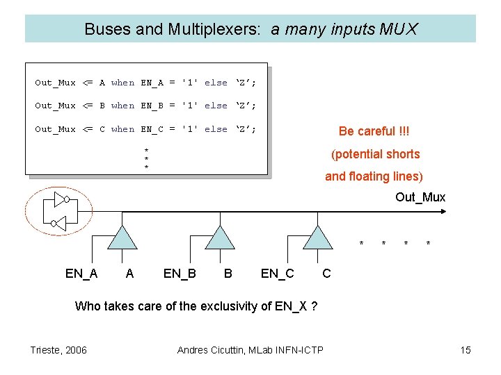
Buses and Multiplexers: a many inputs MUX Out_Mux <= A when EN_A = '1' else ‘Z’; Out_Mux <= B when EN_B = '1' else ‘Z’; Out_Mux <= C when EN_C = '1' else ‘Z’; Be careful !!! * * * (potential shorts and floating lines) Out_Mux * EN_A A EN_B B EN_C * * * C Who takes care of the exclusivity of EN_X ? Trieste, 2006 Andres Cicuttin, MLab INFN-ICTP 15

Part B. FPGA Design • The synchronous design • Avoidable and Unavoidable asynchronous designs • Special asynchronous circuits • Debugging Techniques • Common mistakes • Good design practices Trieste, 2006 Andres Cicuttin, MLab INFN-ICTP 16

The Ideal Synchronous Design • The timing of the whole design is referred to a single free running clock (or multiple clocks from a common source with perfectly controlled inter-clock phase) Trieste, 2006 Andres Cicuttin, MLab INFN-ICTP 17

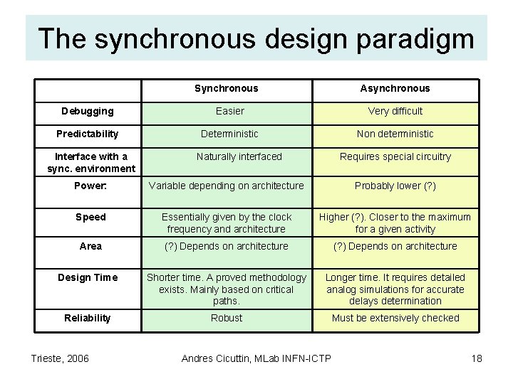
The synchronous design paradigm Synchronous Asynchronous Debugging Easier Very difficult Predictability Deterministic Non deterministic Interface with a sync. environment Naturally interfaced Requires special circuitry Power: Variable depending on architecture Probably lower (? ) Speed Essentially given by the clock frequency and architecture Higher (? ). Closer to the maximum for a given activity Area (? ) Depends on architecture Design Time Shorter time. A proved methodology exists. Mainly based on critical paths. Longer time. It requires detailed analog simulations for accurate delays determination Reliability Robust Must be extensively checked Trieste, 2006 Andres Cicuttin, MLab INFN-ICTP 18

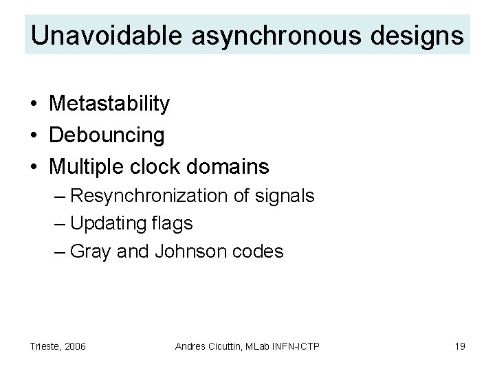
Unavoidable asynchronous designs • Metastability • Debouncing • Multiple clock domains – Resynchronization of signals – Updating flags – Gray and Johnson codes Trieste, 2006 Andres Cicuttin, MLab INFN-ICTP 19

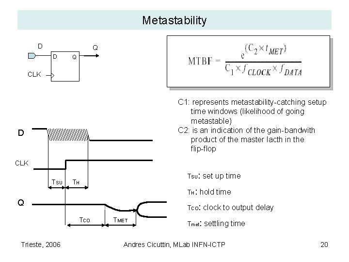
Metastability D Q CLK C 1: represents metastability-catching setup time windows (likelihood of going metastable) C 2: is an indication of the gain-bandwith product of the master lacth in the flip-flop D CLK TSU: set up time TH TH: hold time Q TCO: clock to output delay TCO Trieste, 2006 TMET Tmet: settling time Andres Cicuttin, MLab INFN-ICTP 20

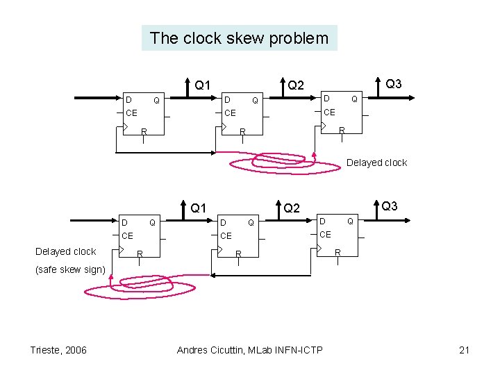
The clock skew problem Q 1 D D Q CE Q 3 Q 2 D Q CE CE R Q R R Delayed clock Q 1 D Q CE Delayed clock D Q CE CE R Q 3 Q 2 R R (safe skew sign) Trieste, 2006 Andres Cicuttin, MLab INFN-ICTP 21

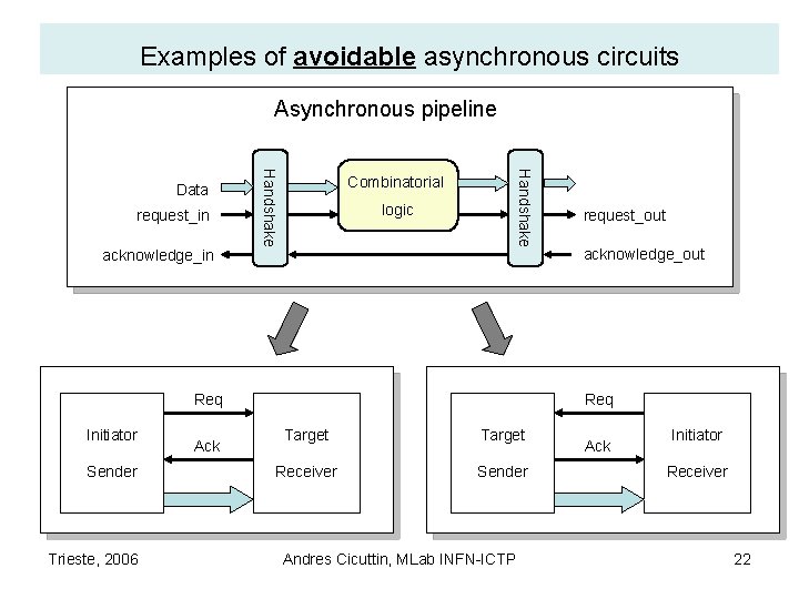
Examples of avoidable asynchronous circuits Asynchronous pipeline acknowledge_in Handshake request_in Handshake Data Combinatorial logic Req Initiator Sender Trieste, 2006 Ack request_out acknowledge_out Req Target Receiver Sender Andres Cicuttin, MLab INFN-ICTP Ack Initiator Receiver 22

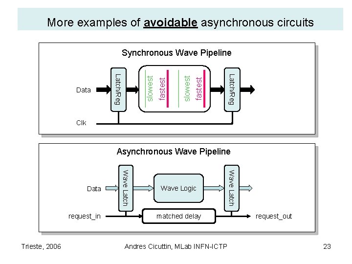
More examples of avoidable asynchronous circuits fastest slowest Latch/Reg Data fastest Synchronous Wave Pipeline Clk Asynchronous Wave Pipeline Trieste, 2006 Wave Logic matched delay Andres Cicuttin, MLab INFN-ICTP Wave Latch request_in Wave Latch Data request_out 23

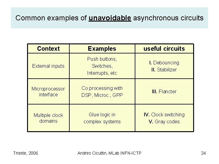
Common examples of unavoidable asynchronous circuits Context Examples useful circuits External inputs Push buttons, Switches, Interrupts, etc I. Debouncing II. Stabilizer Microprocessor interface Co processing with DSP, Microc. , GPP III. Flancter Multiple clock domains Glue logic in complex systems IV. Clock switching V. Gray codes Trieste, 2006 Andres Cicuttin, MLab INFN-ICTP 24

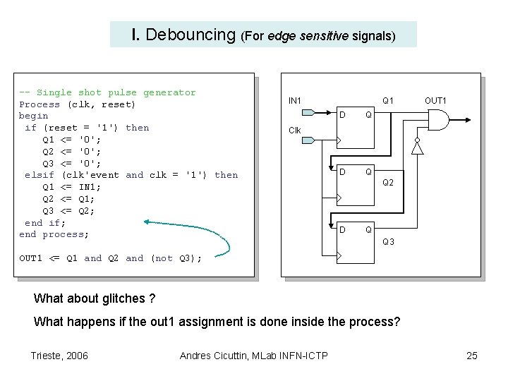
I. Debouncing (For edge sensitive signals) -- Single shot pulse generator Process (clk, reset) begin if (reset = '1') then Q 1 <= '0'; Q 2 <= '0'; Q 3 <= '0'; elsif (clk'event and clk = '1') then Q 1 <= IN 1; Q 2 <= Q 1; Q 3 <= Q 2; end if; end process; IN 1 Q 1 D Q OUT 1 Clk Q 2 D Q Q 3 OUT 1 <= Q 1 and Q 2 and (not Q 3); What about glitches ? What happens if the out 1 assignment is done inside the process? Trieste, 2006 Andres Cicuttin, MLab INFN-ICTP 25

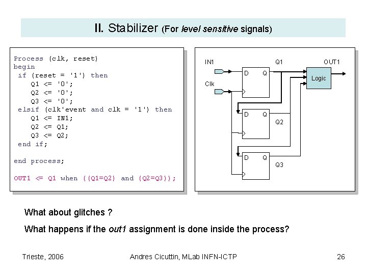
II. Stabilizer (For level sensitive signals) Process (clk, reset) begin if (reset = '1') then Q 1 <= '0'; Q 2 <= '0'; Q 3 <= '0'; elsif (clk'event and clk = '1') then Q 1 <= IN 1; Q 2 <= Q 1; Q 3 <= Q 2; end if; IN 1 Q 1 D Q Logic Clk Q 2 D end process; OUT 1 Q Q 3 OUT 1 <= Q 1 when ((Q 1=Q 2) and (Q 2=Q 3)); What about glitches ? What happens if the out 1 assignment is done inside the process? Trieste, 2006 Andres Cicuttin, MLab INFN-ICTP 26

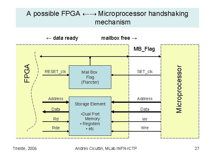
A possible FPGA ←→ Microprocessor handshaking mechanism ← data ready mailbox free → RESET_clk Mail Box Flag (Flancter) Address SET_clk Address Storage Element Data Rd Rde Trieste, 2006 • Dual Port Memory • Registers • etc Andres Cicuttin, MLab INFN-ICTP Data Microprocessor FPGA MB_Flag Wr Wre 27

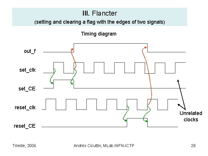
III. Flancter (setting and clearing a flag with the edges of two signals) Timing diagram out_f set_clk set_CE reset_clk Unrelated clocks reset_CE Trieste, 2006 Andres Cicuttin, MLab INFN-ICTP 28

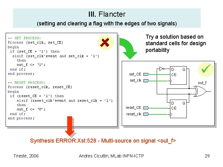
III. Flancter (setting and clearing a flag with the edges of two signals) -- SET PROCESS: Process (set_clk, set_CE) begin if (set_CE = '1') then elsif (set_clk'event and set_clk = '1') then out_f <= ‘ 1’; end if; end process; -- RESET PROCESS: Process (reset_clk, reset_CE) begin if (reset_CE = '1') then elsif (reset_clk'event and reset_clk = '1') then out_f <= ‘ 0’; end if; end process; Try a solution based on standard cells for design portability set_CE D CE Q set_clk reset_CE ü. out_f D CE Q reset_clk Synthesis ERROR: Xst: 528 - Multi-source on signal <out_f> Trieste, 2006 Andres Cicuttin, MLab INFN-ICTP 29

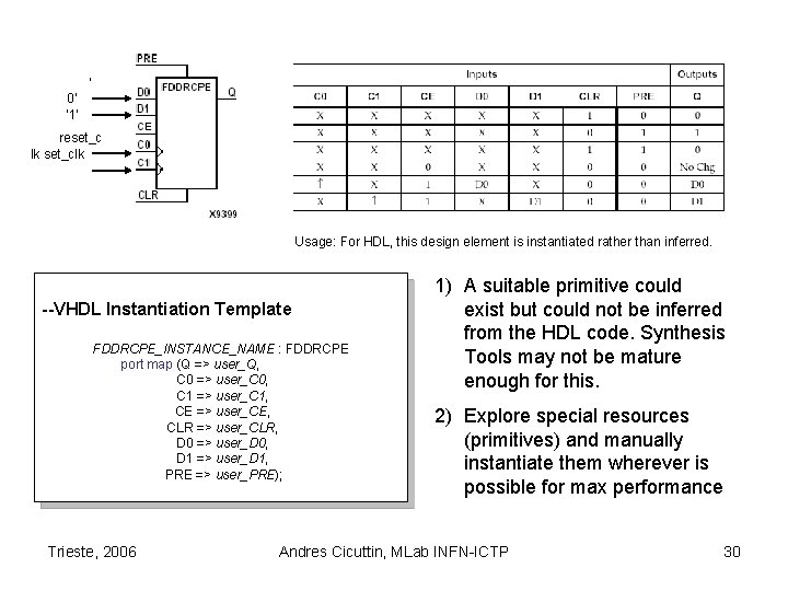
‘ 0’ ‘ 1’ reset_c lk set_clk Usage: For HDL, this design element is instantiated rather than inferred. --VHDL Instantiation Template FDDRCPE_INSTANCE_NAME : FDDRCPE port map (Q => user_Q, C 0 => user_C 0, C 1 => user_C 1, CE => user_CE, CLR => user_CLR, D 0 => user_D 0, D 1 => user_D 1, PRE => user_PRE); Trieste, 2006 1) A suitable primitive could exist but could not be inferred from the HDL code. Synthesis Tools may not be mature enough for this. 2) Explore special resources (primitives) and manually instantiate them wherever is possible for max performance Andres Cicuttin, MLab INFN-ICTP 30

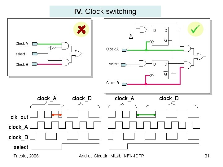
IV. Clock switching D Q ü Q Clock A select Clock B D Q Q Clock B clock_A clock_B clk_out clock_A clock_B select Trieste, 2006 Andres Cicuttin, MLab INFN-ICTP 31

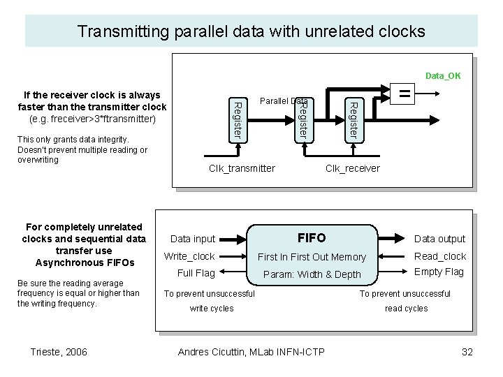
Transmitting parallel data with unrelated clocks Data_OK Be sure the reading average frequency is equal or higher than the writing frequency. Trieste, 2006 Clk_transmitter Data input Write_clock Full Flag Register For completely unrelated clocks and sequential data transfer use Asynchronous FIFOs Parallel Data Register This only grants data integrity. Doesn’t prevent multiple reading or overwriting Register If the receiver clock is always faster than the transmitter clock (e. g. freceiver>3*ftransmitter) = Clk_receiver FIFO Data output First In First Out Memory Read_clock Param: Width & Depth Empty Flag To prevent unsuccessful write cycles read cycles Andres Cicuttin, MLab INFN-ICTP 32

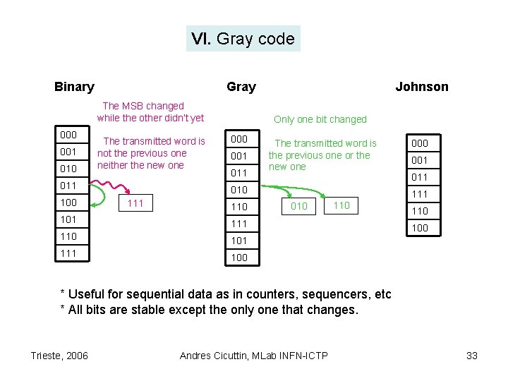
VI. Gray code Binary Gray The MSB changed while the other didn’t yet 000 001 010 The transmitted word is not the previous one neither the new one 011 100 Johnson Only one bit changed 000 001 011 The transmitted word is the previous one or the new one 010 111 110 101 111 100 001 011 111 010 110 100 * Useful for sequential data as in counters, sequencers, etc * All bits are stable except the only one that changes. Trieste, 2006 Andres Cicuttin, MLab INFN-ICTP 33

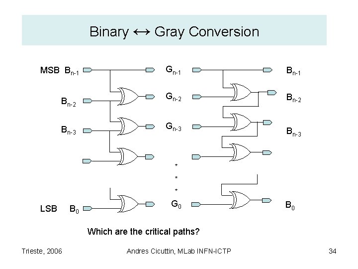
Binary ↔ Gray Conversion MSB Bn-1 Bn-2 Bn-3 Gn-1 Bn-1 Gn-2 Bn-2 Gn-3 Bn-3 * * * LSB B 0 G 0 B 0 Which are the critical paths? Trieste, 2006 Andres Cicuttin, MLab INFN-ICTP 34

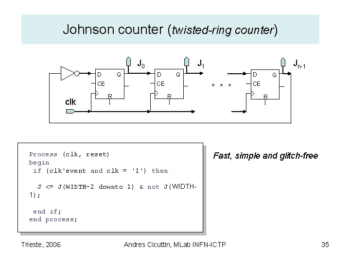
Johnson counter (twisted-ring counter) J 0 D Q CE clk J 1 D Q CE R Jn-1 D * * * R Process (clk, reset) begin if (clk'event and clk = '1') then Q CE R Fast, simple and glitch-free J <= J(WIDTH-2 downto 1) & not J(WIDTH 1); end if; end process; Trieste, 2006 Andres Cicuttin, MLab INFN-ICTP 35

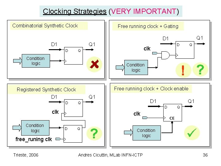
Clocking Strategies (VERY IMPORTANT) Combinatorial Synthetic Clock Free running clock + Gating Q 1 D 1 Q 1 D D Free running clock + Clock enable Q 1 free_runing clk D 1 Q Q 1 D clk Condition logic clk D Q ! ? Condition logic Registered Synthetic Clock D 1 Trieste, 2006 clk Q Condition logic D Q ? Condition logic Andres Cicuttin, MLab INFN-ICTP Q CE ü 36

Debugging Techniques • Seeing and controlling internal signals • FSM debugging • In chip logic analysis Trieste, 2006 Andres Cicuttin, MLab INFN-ICTP 37

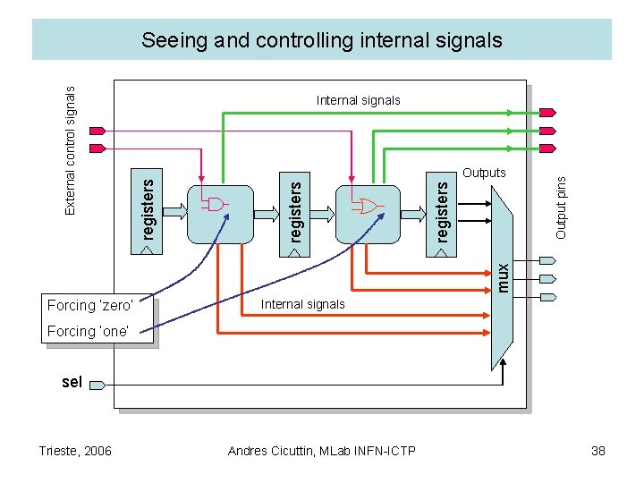
mux registers Outputs Output pins Internal signals registers External control signals Seeing and controlling internal signals Forcing ‘zero’ Internal signals Forcing ‘one’ sel Trieste, 2006 Andres Cicuttin, MLab INFN-ICTP 38

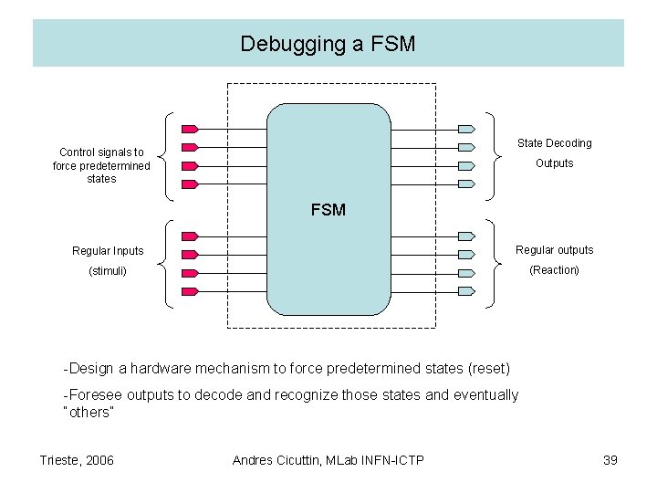
Debugging a FSM State Decoding Control signals to force predetermined states Outputs FSM Regular Inputs Regular outputs (stimuli) (Reaction) -Design a hardware mechanism to force predetermined states (reset) -Foresee outputs to decode and recognize those states and eventually “others” Trieste, 2006 Andres Cicuttin, MLab INFN-ICTP 39

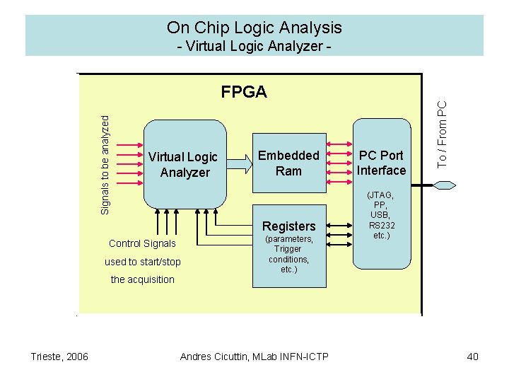
On Chip Logic Analysis Signals to be analyzed FPGA Virtual Logic Analyzer Embedded Ram Registers Control Signals used to start/stop the acquisition Trieste, 2006 (parameters, Trigger conditions, etc. ) Andres Cicuttin, MLab INFN-ICTP PC Port Interface To / From PC - Virtual Logic Analyzer - (JTAG, PP, USB, RS 232 etc. ) 40

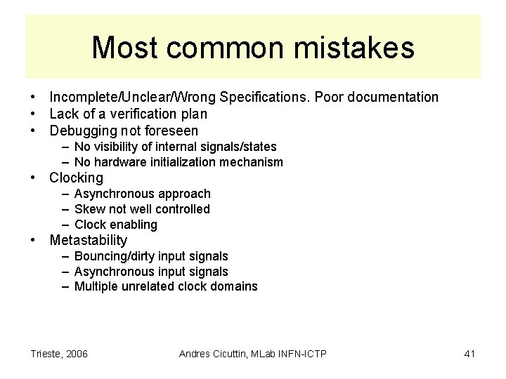
Most common mistakes • Incomplete/Unclear/Wrong Specifications. Poor documentation • Lack of a verification plan • Debugging not foreseen – No visibility of internal signals/states – No hardware initialization mechanism • Clocking – Asynchronous approach – Skew not well controlled – Clock enabling • Metastability – Bouncing/dirty input signals – Asynchronous input signals – Multiple unrelated clock domains Trieste, 2006 Andres Cicuttin, MLab INFN-ICTP 41

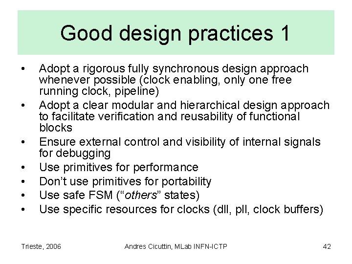
Good design practices 1 • • Adopt a rigorous fully synchronous design approach whenever possible (clock enabling, only one free running clock, pipeline) Adopt a clear modular and hierarchical design approach to facilitate verification and reusability of functional blocks Ensure external control and visibility of internal signals for debugging Use primitives for performance Don’t use primitives for portability Use safe FSM (“others” states) Use specific resources for clocks (dll, pll, clock buffers) Trieste, 2006 Andres Cicuttin, MLab INFN-ICTP 42

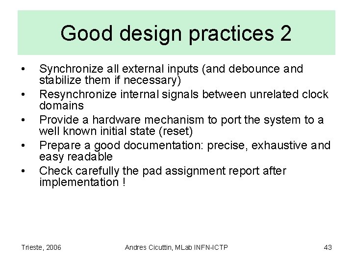
Good design practices 2 • • • Synchronize all external inputs (and debounce and stabilize them if necessary) Resynchronize internal signals between unrelated clock domains Provide a hardware mechanism to port the system to a well known initial state (reset) Prepare a good documentation: precise, exhaustive and easy readable Check carefully the pad assignment report after implementation ! Trieste, 2006 Andres Cicuttin, MLab INFN-ICTP 43