SEE 2063 Electronic Devices Introduction Field effect transistors

- Slides: 19

SEE 2063 Electronic Devices

Introduction • Field effect transistors are unipolar devices that control current by voltage applied to the gate. • Two main types of FETs are JFET and MOSFET • The FET’s major advantage over the BJT is high input resistance. • Overall, the purpose of the FET is the same as that of the BJT. 2

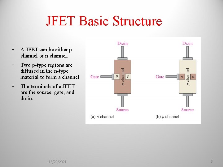
JFET Basic Structure • A JFET can be either p channel or n channel. • Two p-type regions are diffused in the n-type material to form a channel • The terminals of a JFET are the source, gate, and drain. 12/22/2021 3

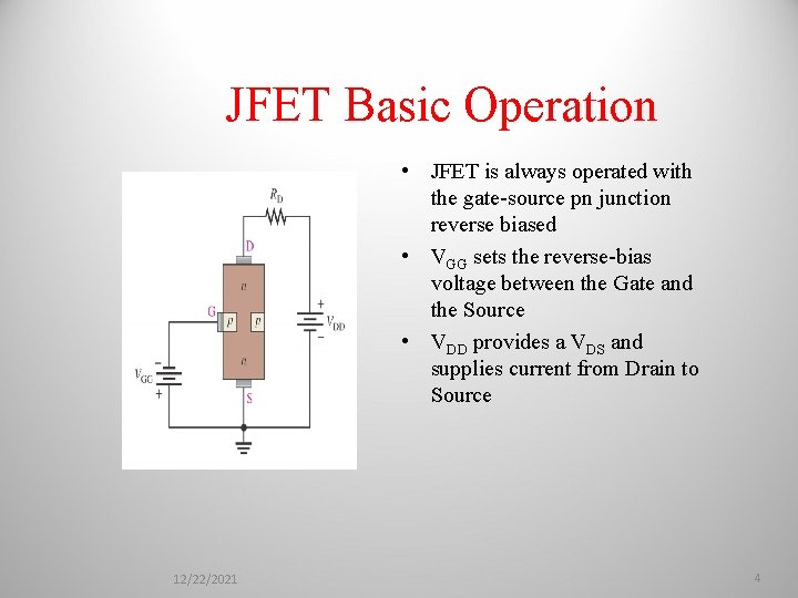
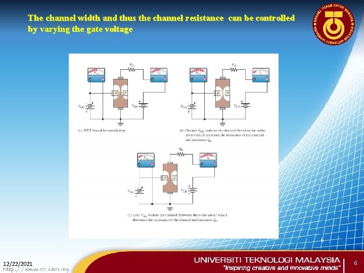
JFET Basic Operation • JFET is always operated with the gate-source pn junction reverse biased • VGG sets the reverse-bias voltage between the Gate and the Source • VDD provides a VDS and supplies current from Drain to Source 12/22/2021 4

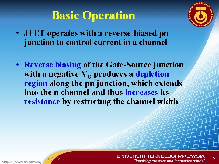
Basic Operation • JFET operates with a reverse-biased pn junction to control current in a channel • Reverse biasing of the Gate-Source junction with a negative VG produces a depletion region along the pn junction, which extends into the n channel and thus increases its resistance by restricting the channel width 12/22/2021 5

The channel width and thus the channel resistance can be controlled by varying the gate voltage 6 12/22/2021 6

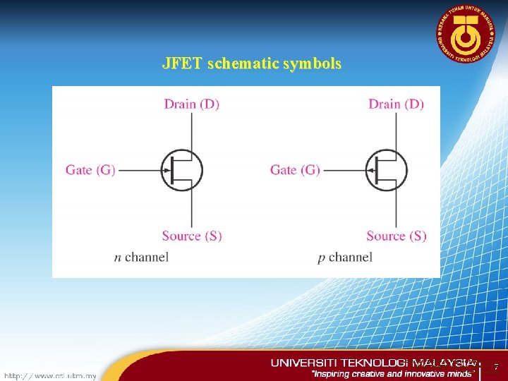
JFET schematic symbols 7 Copyright © 2005 by Pearson Education, Inc. Upper Saddle River, New Jersey 07458 All rights reserved. 7

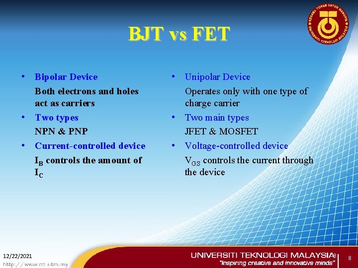
BJT vs FET • Bipolar Device Both electrons and holes act as carriers • Two types NPN & PNP • Current-controlled device IB controls the amount of IC 12/22/2021 • Unipolar Device Operates only with one type of charge carrier • Two main types JFET & MOSFET • Voltage-controlled device VGS controls the current through the device 8 8

SUMMARY • FETs are unipolar devices (one-charge carrier) • The three FET terminals are source, drain, and gate • The JFET operates with a reverse-biased pn junction (gate -to-source) • The high input resistance of a JFET is due to reversebiased gate-source junction • Reverse bias of a JFET produces a depletion region within the channel, thus increasing channel resistance 12/22/2021 9

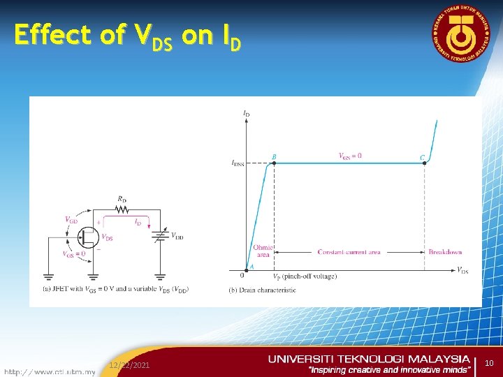
Effect of VDS on ID 12/22/2021 10

Drain Characteristics (VGS = 0 V) • For a small value of VDS, JFET behaves as a simple resistor between the D and the S. • As VDS increases from 0 V, ID increases in an approximately linear manner (ohm’s law) • As VDS continue to increase, noticeable depletion regions begin to form in the channel • Depletion regions are broader near the drain end of the channel • Total resistance of the channel is increased • The rise in current is no longer proportional to VDS • The current begins to level off 11

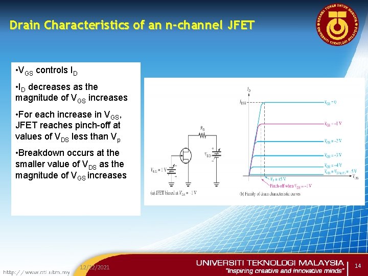
…. Drain Characteristics (VGS = 0 V) • As VDS increases to a value known as the pinch-off voltage (Vp), the depletion region increases to the point where the conducting channel at the drain end is completely pinch-off • The current reaches a maximum value (IDSS) at pinch-off and that it continues to flow at that value as VDS is increased beyond Vp • Breakdown occurs at large values of VDS and is caused by the avalanche mechanism • At breakdown, ID begins to increase very rapidly with any further increase in VDs • Breakdown can result in irreversible damage to the device 12/22/2021 12

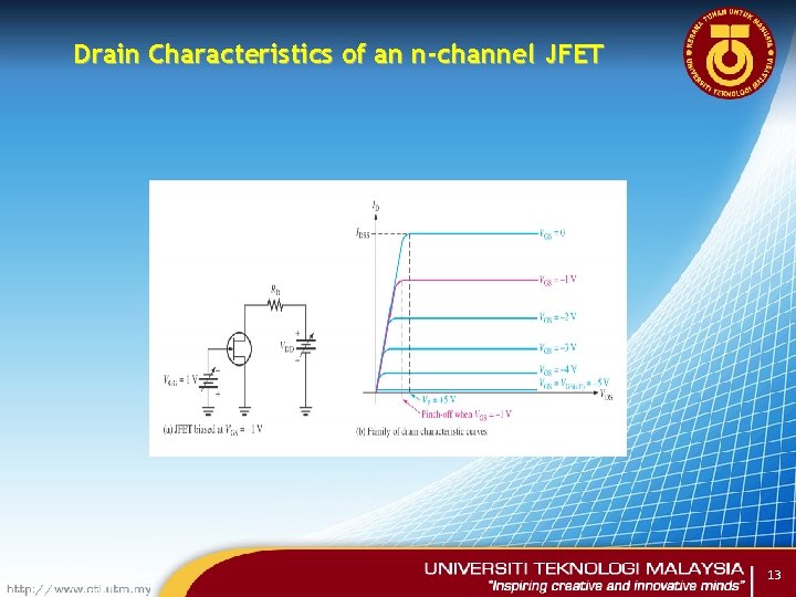
Drain Characteristics of an n-channel JFET 13

Drain Characteristics of an n-channel JFET • VGS controls ID • ID decreases as the magnitude of VGS increases • For each increase in VGS, JFET reaches pinch-off at values of VDS less than Vp • Breakdown occurs at the smaller value of VDS as the magnitude of VGS increases 12/22/2021 14

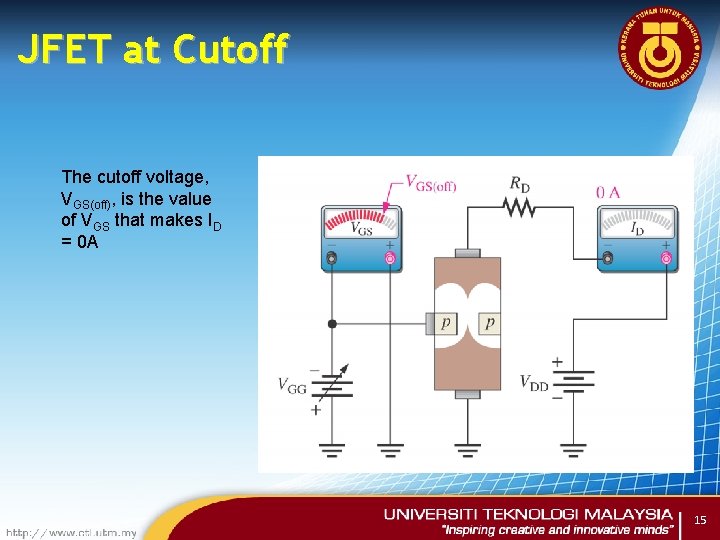
JFET at Cutoff The cutoff voltage, VGS(off), is the value of VGS that makes ID = 0 A 15

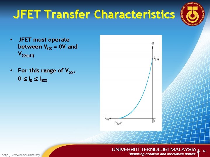
JFET Transfer Characteristics • JFET must operate between VGS = 0 V and VGS(off) • For this range of VGS, 0 IDSS 16 16

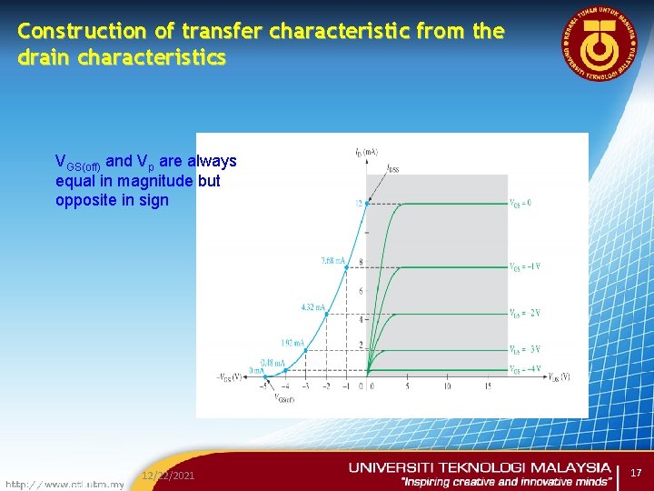
Construction of transfer characteristic from the drain characteristics VGS(off) and Vp are always equal in magnitude but opposite in sign 12/22/2021 17

JFET Parameters • • • Ohmic Area (Voltage-Controlled Resistance Region) An area where VDS and ID are related by Ohm’s Law Pinch-Off Voltage, Vp The value of VDS at which ID becomes constant when VGS = 0 V IDSS The Drain to Source current with the gate Shorted (VGS = 0 V) Constant-Current Area (Pinch-Off Region, Active Region, Saturation Region ) The region in which the JFET is normally operated when used for small-signal amplification Cut-Off Voltage The value of VGS at which ID becomes zero 12/22/2021 18

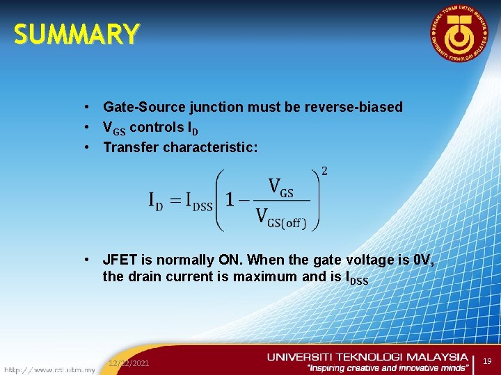
SUMMARY • Gate-Source junction must be reverse-biased • VGS controls ID • Transfer characteristic: • JFET is normally ON. When the gate voltage is 0 V, the drain current is maximum and is IDSS 12/22/2021 19