Section 8 Metallization Jaeger Chapter 7 EE 143

- Slides: 20

Section 8: Metallization Jaeger Chapter 7 EE 143 – Ali Javey

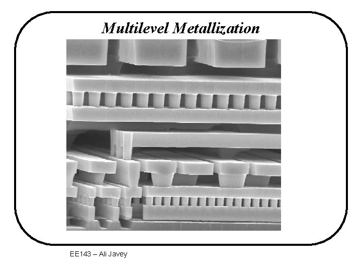
Multilevel Metallization EE 143 – Ali Javey

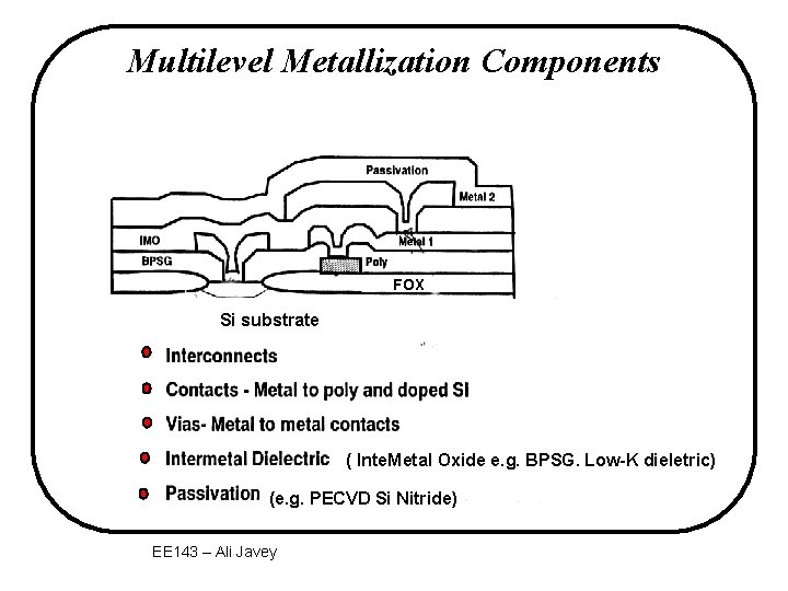
Multilevel Metallization Components FOX Si substrate ( Inte. Metal Oxide e. g. BPSG. Low-K dieletric) (e. g. PECVD Si Nitride) EE 143 – Ali Javey

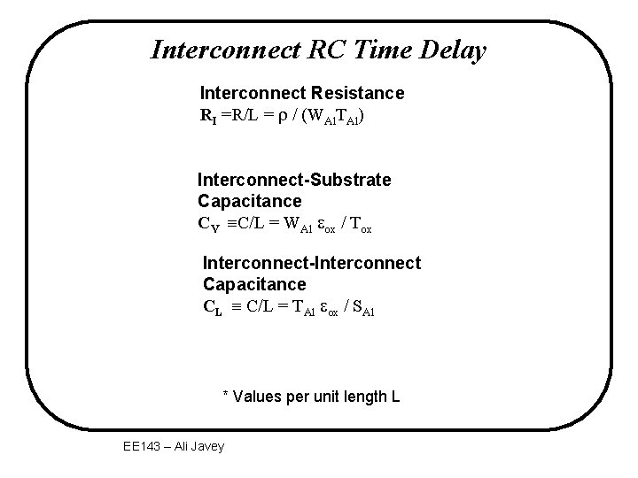
Interconnect RC Time Delay Interconnect Resistance RI =R/L = / (WAl. TAl) Interconnect-Substrate Capacitance CV C/L = WAl ox / Tox Interconnect-Interconnect Capacitance CL C/L = TAl ox / SAl * Values per unit length L EE 143 – Ali Javey

Interconnect Requirements • low ohmic resistance – interconnects material has low resistivity • low contact resistance to semiconductor device • reliable long-term operation EE 143 – Ali Javey

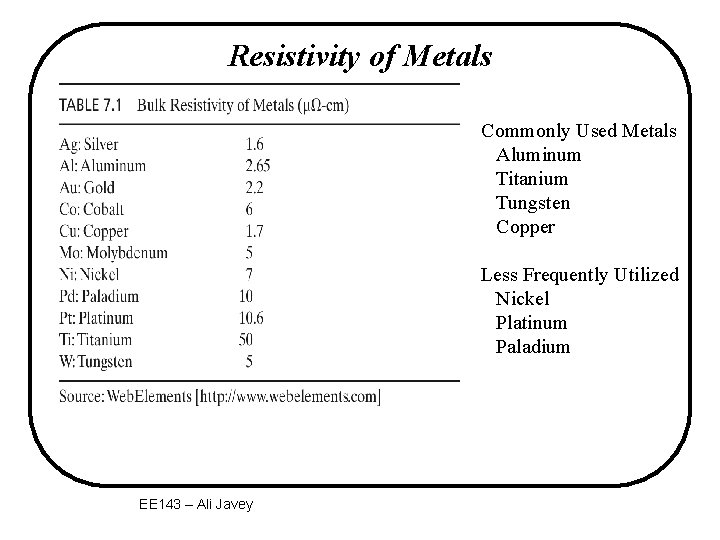
Resistivity of Metals Commonly Used Metals Aluminum Titanium Tungsten Copper Less Frequently Utilized Nickel Platinum Paladium EE 143 – Ali Javey

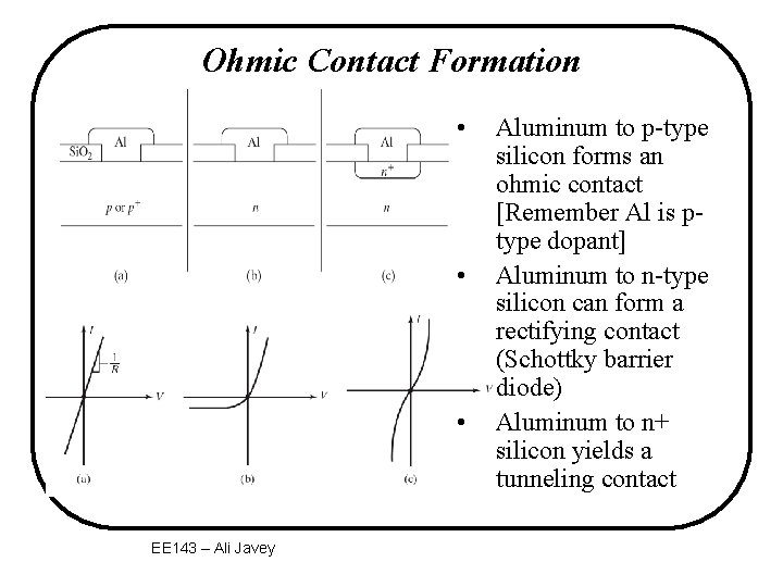
Ohmic Contact Formation • • • EE 143 – Ali Javey Aluminum to p-type silicon forms an ohmic contact [Remember Al is ptype dopant] Aluminum to n-type silicon can form a rectifying contact (Schottky barrier diode) Aluminum to n+ silicon yields a tunneling contact

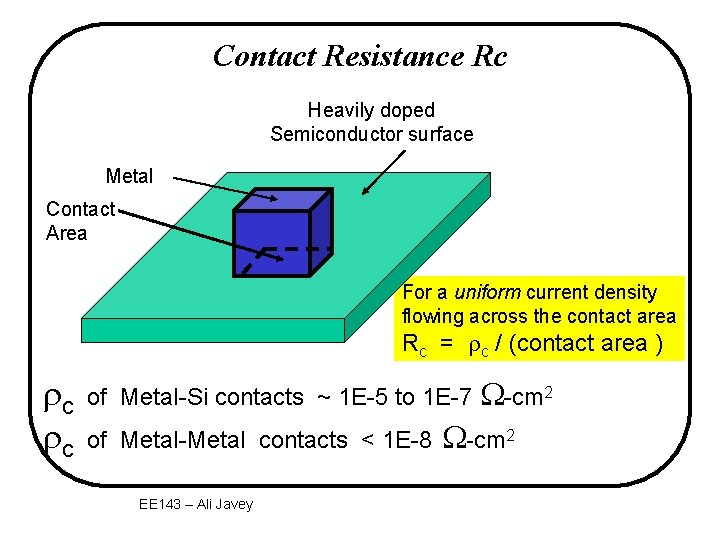
Contact Resistance Rc Heavily doped Semiconductor surface Metal Contact Area For a uniform current density flowing across the contact area Rc = c / (contact area ) c c of Metal-Si contacts ~ 1 E-5 to 1 E-7 W-cm 2 of Metal-Metal contacts < 1 E-8 EE 143 – Ali Javey W-cm 2

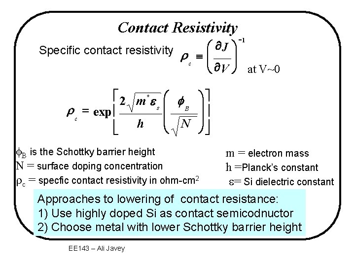
Contact Resistivity -1 Specific contact resistivity r º æ ¶ J ö ç ÷ c è ¶ V ø at V~0 é 2 m *e s r c = exp ê h êë æ f ç B ç N è B is the Schottky barrier height N = surface doping concentration c = specfic contact resistivity in ohm-cm 2 öù ÷ú ÷ ø úû m = electron mass h =Planck’s constant = Si dielectric constant Approaches to lowering of contact resistance: 1) Use highly doped Si as contact semicodnuctor 2) Choose metal with lower Schottky barrier height EE 143 – Ali Javey

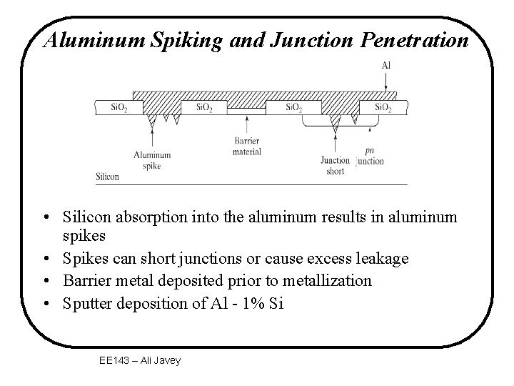
Aluminum Spiking and Junction Penetration • Silicon absorption into the aluminum results in aluminum spikes • Spikes can short junctions or cause excess leakage • Barrier metal deposited prior to metallization • Sputter deposition of Al - 1% Si EE 143 – Ali Javey

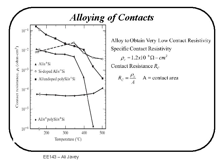
Alloying of Contacts EE 143 – Ali Javey

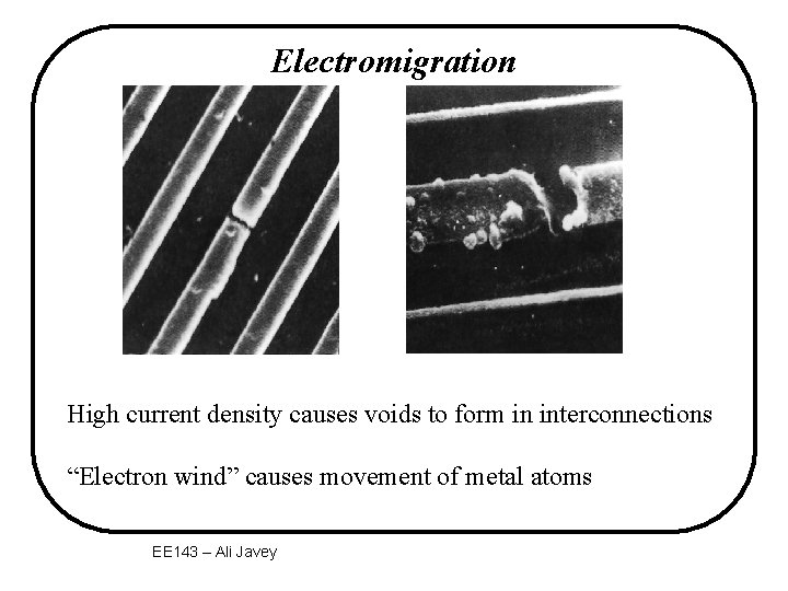
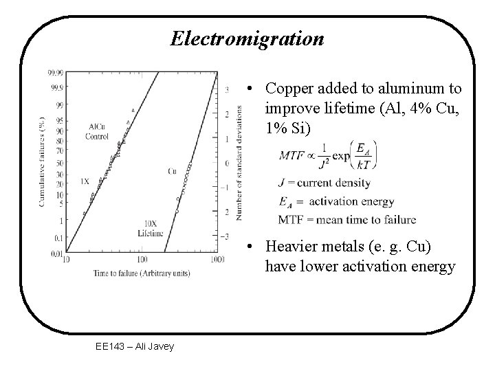
Electromigration High current density causes voids to form in interconnections “Electron wind” causes movement of metal atoms EE 143 – Ali Javey

Electromigration • Copper added to aluminum to improve lifetime (Al, 4% Cu, 1% Si) • Heavier metals (e. g. Cu) have lower activation energy EE 143 – Ali Javey

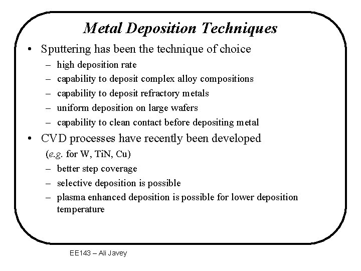
Metal Deposition Techniques • Sputtering has been the technique of choice – – – high deposition rate capability to deposit complex alloy compositions capability to deposit refractory metals uniform deposition on large wafers capability to clean contact before depositing metal • CVD processes have recently been developed (e. g. for W, Ti. N, Cu) – better step coverage – selective deposition is possible – plasma enhanced deposition is possible for lower deposition temperature EE 143 – Ali Javey

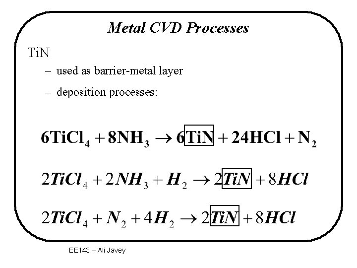
Metal CVD Processes Ti. N – used as barrier-metal layer – deposition processes: EE 143 – Ali Javey

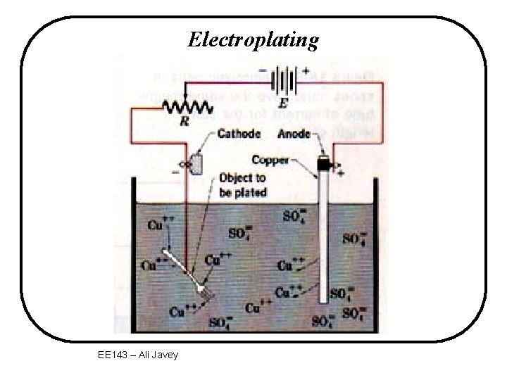
Electroplating EE 143 – Ali Javey

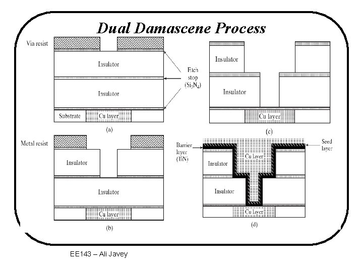
Dual Damascene Process EE 143 – Ali Javey

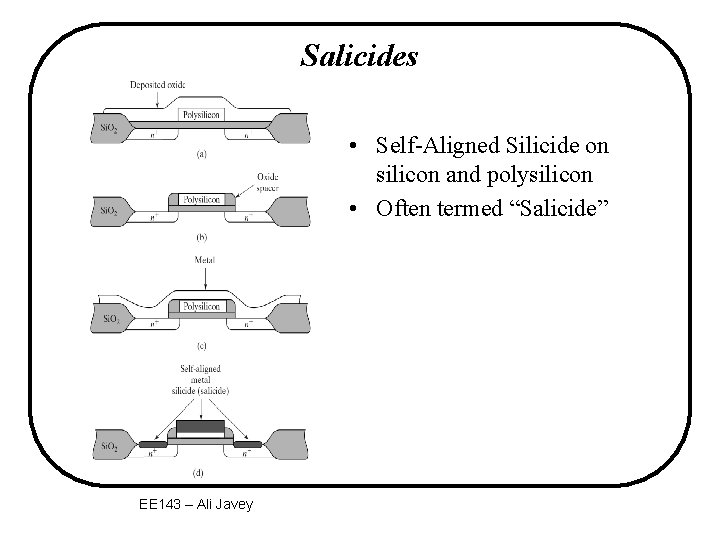
Salicides • Self-Aligned Silicide on silicon and polysilicon • Often termed “Salicide” EE 143 – Ali Javey

Low-K Dielectrics EE 143 – Ali Javey

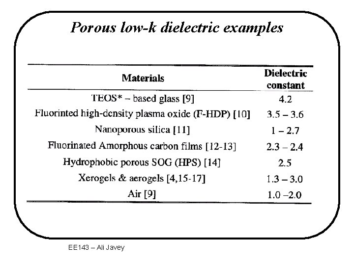
Porous low-k dielectric examples EE 143 – Ali Javey