Secrets of the DCM Part 1 Steve Knapp





- Slides: 56

Secrets of the DCM: Part 1 Steve Knapp General Products Division (steve. knapp@xilinx. com) スティーブ・ナップ NOTICE: This is an early draft of this presentation. Please visit the Xilinx Sales Partner Web (SPW) for the latest version. http: //www. partner. xilinx. com/common/spartan 3/fae © 2004 by Xilinx, Inc. All rights reserved. (v 1. 2, 11 -OCT-2004)

Workshop Objectives By the end of this class, you will … • Understand the function and application of Digital Clock Managers (DCMs) • Unlock a few mysteries on how DCMs operate – More mysteries revealed in Part II • Become a Clock Wizard and easily configure a DCM • Have a few new approaches to teach customers on DCMs • Legitimately say “DCMs Don’t Confuse Me” Secrets of the DCM (Part I) 2

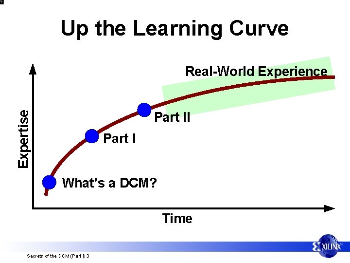
Up the Learning Curve Expertise Real-World Experience Part II Part I What’s a DCM? Time Secrets of the DCM (Part I) 3

DCMs Everywhere! • In this presentation, the Spartan-3 DCM demonstrates basic principals and concepts • The Spartan-3 DCM is similar to Virtex-II and Virtex-II Pro • The DLL in the DCM is similar to the DLL in Virtex/E and Spartan-II/E • Virtex-4 DCM also employees similar concepts Secrets of the DCM (Part I) 4

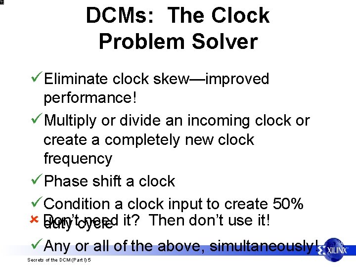
DCMs: The Clock Problem Solver üEliminate clock skew—improved performance! üMultiply or divide an incoming clock or create a completely new clock frequency üPhase shift a clock üCondition a clock input to create 50% Don’t need it? Then don’t use it! duty cycle üAny or all of the above, simultaneously! Secrets of the DCM (Part I) 5

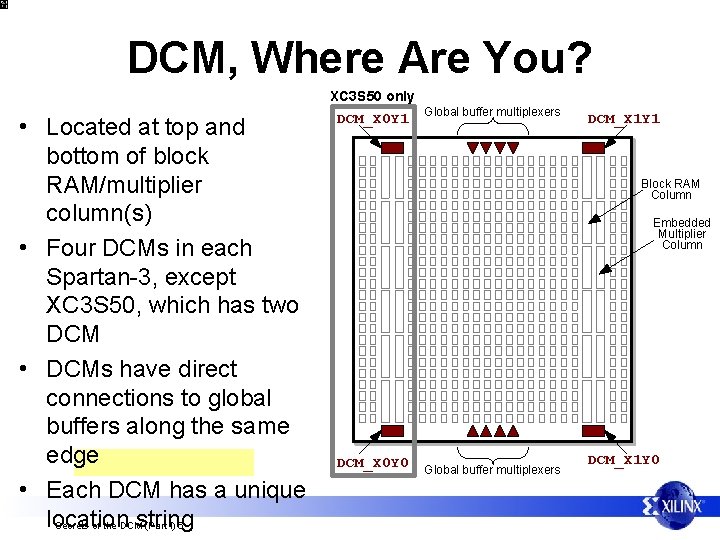
DCM, Where Are You? XC 3 S 50 only • Located at top and bottom of block RAM/multiplier column(s) • Four DCMs in each Spartan-3, except XC 3 S 50, which has two DCM • DCMs have direct connections to global buffers along the same edge • Each DCM has a unique location string Secrets of the DCM (Part I) 6 DCM_X 0 Y 1 Global buffer multiplexers DCM_X 1 Y 1 Block RAM Column Embedded Multiplier Column DCM_X 0 Y 0 Global buffer multiplexers DCM_X 1 Y 0

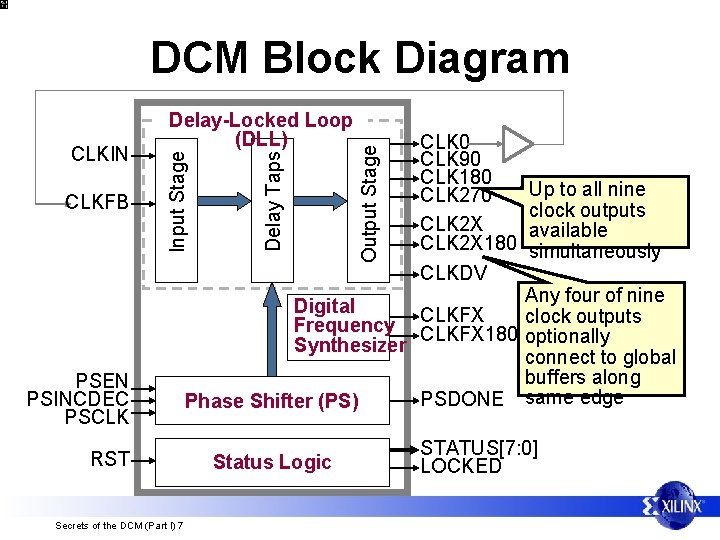
Delay Taps CLKFB Input Stage CLKIN Delay-Locked Loop (DLL) DCM PSEN PSINCDEC PSCLK RST Secrets of the DCM (Part I) 7 Output Stage DCM Block Diagram CLK 0 CLK 90 CLK 180 CLK 270 CLK 2 X 180 CLKDV Up to all nine clock outputs available simultaneously Any four of nine Digital CLKFX Frequency CLKFX 180 clock outputs optionally Synthesizer connect to global buffers along PSDONE same edge Phase Shifter (PS) Status Logic STATUS[7: 0] LOCKED

Lesson One Avoid being skewed!

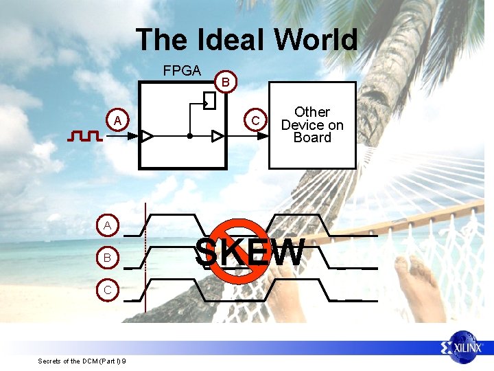
The Ideal World FPGA A A B C Secrets of the DCM (Part I) 9 B C Other Device on Board SKEW

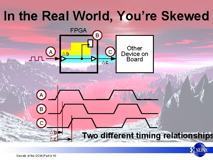
In the Real World, You’re Skewed FPGA A B C Db Dc Other Device on Board A B C Db Dc Secrets of the DCM (Part I) 10 Two different timing relationships

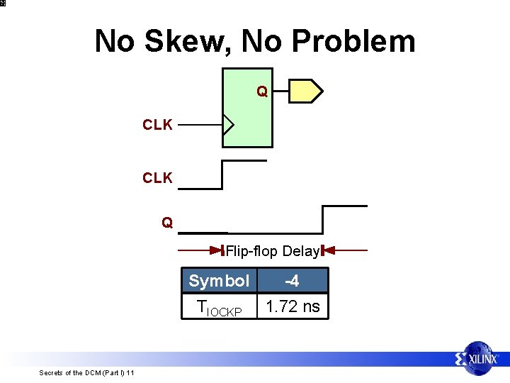
No Skew, No Problem Q CLK Q Flip-flop Delay Symbol -4 TIOCKP 1. 72 ns Secrets of the DCM (Part I) 11

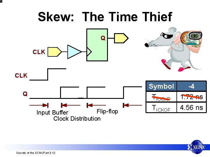
Skew: The Time Thief Q CLK Symbol -4 TIOCKP 1. 72 ns Q Flip-flop Input Buffer Clock Distribution Secrets of the DCM (Part I) 12 TICKOF 4. 56 ns

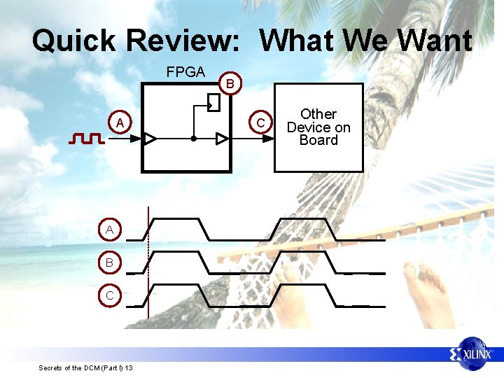
Quick Review: What We Want FPGA A A B C Secrets of the DCM (Part I) 13 B C Other Device on Board

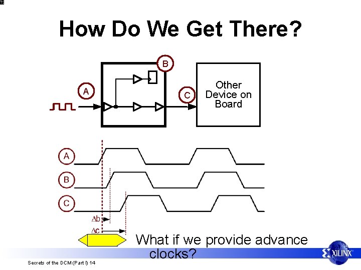
How Do We Get There? B A Secrets of the DCM (Part I) 14 C Other Device on Board What if we provide advance clocks?

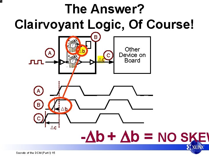
The Answer? Clairvoyant Logic, Of Course! B Db A Dc C Other Device on Board A B Db C Dc Secrets of the DCM (Part I) 15 -Db + Db = NO SKEW

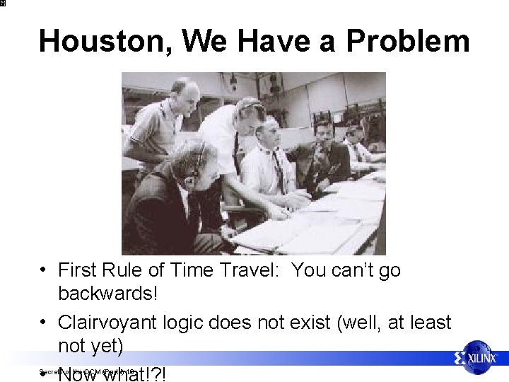
Houston, We Have a Problem • First Rule of Time Travel: You can’t go backwards! • Clairvoyant logic does not exist (well, at least not yet) • Now what!? ! Secrets of the DCM (Part I) 16

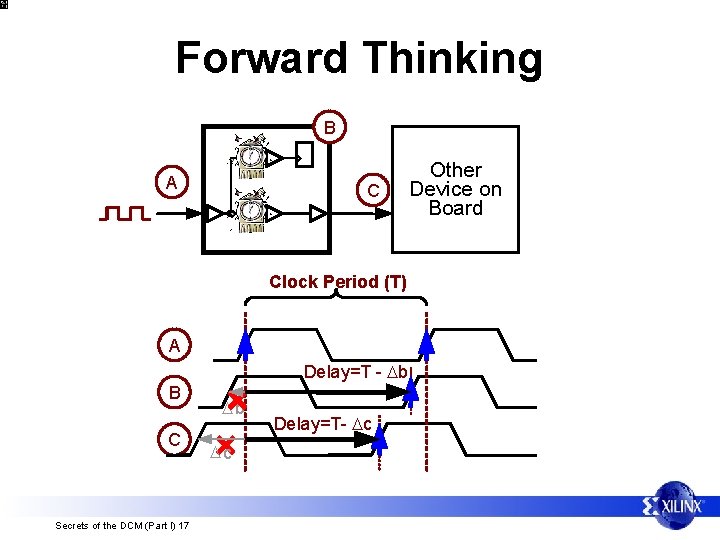
Forward Thinking B A C Clock Period (T) A Delay=T - Db B C Secrets of the DCM (Part I) 17 Db Dc Delay=T- Dc Other Device on Board

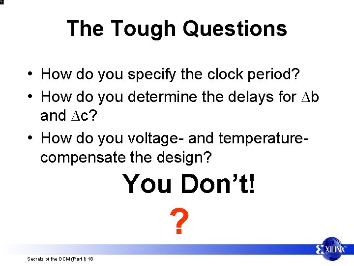
The Tough Questions • How do you specify the clock period? • How do you determine the delays for Db and Dc? • How do you voltage- and temperaturecompensate the design? You Don’t! ? Secrets of the DCM (Part I) 18

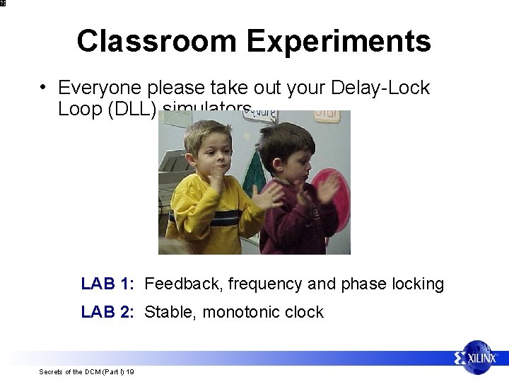
Classroom Experiments • Everyone please take out your Delay-Lock Loop (DLL) simulators LAB 1: Feedback, frequency and phase locking LAB 2: Stable, monotonic clock Secrets of the DCM (Part I) 19

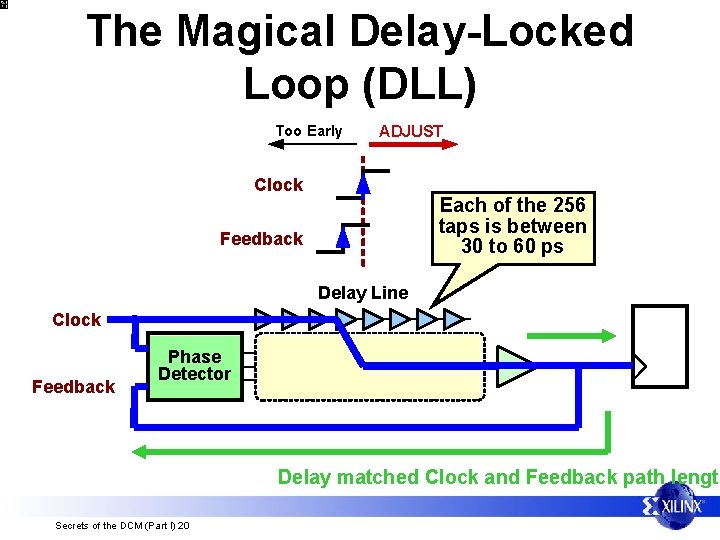
The Magical Delay-Locked Loop (DLL) Too Early ADJUST Clock Each of the 256 taps is between 30 to 60 ps Feedback Delay Line Clock Feedback Phase Detector Delay matched Clock and Feedback path length Secrets of the DCM (Part I) 20

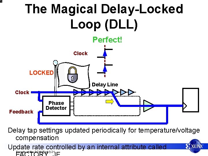
The Magical Delay-Locked Loop (DLL) Perfect! Clock LOCKED Feedback Delay Line Clock Feedback Phase Detector Delay tap settings updated periodically for temperature/voltage compensation Update rate controlled by an internal attribute called Secrets of the DCM (Part I) 21

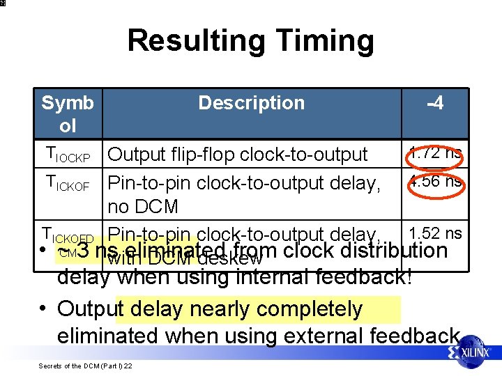
Resulting Timing Symb ol Description -4 TIOCKP 1. 72 ns Output flip-flop clock-to-output TICKOF Pin-to-pin clock-to-output delay, 4. 56 ns no DCM TICKOFD Pin-to-pin clock-to-output delay, 1. 52 ns • ~CM 3 nswith eliminated from clock distribution DCM deskew delay when using internal feedback! • Output delay nearly completely eliminated when using external feedback Secrets of the DCM (Part I) 22

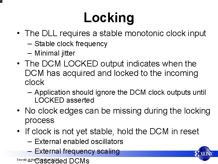
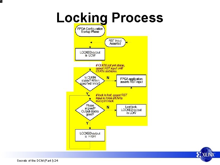
Locking • The DLL requires a stable monotonic clock input – Stable clock frequency – Minimal jitter • The DCM LOCKED output indicates when the DCM has acquired and locked to the incoming clock – Application should ignore the DCM clock outputs until LOCKED asserted • No clock edges can be missing during the locking process • If clock is not yet stable, hold the DCM in reset – External enabled oscillators – External frequency scaling – Cascaded DCMs Secrets of the DCM (Part I) 23

Locking Process Secrets of the DCM (Part I) 24

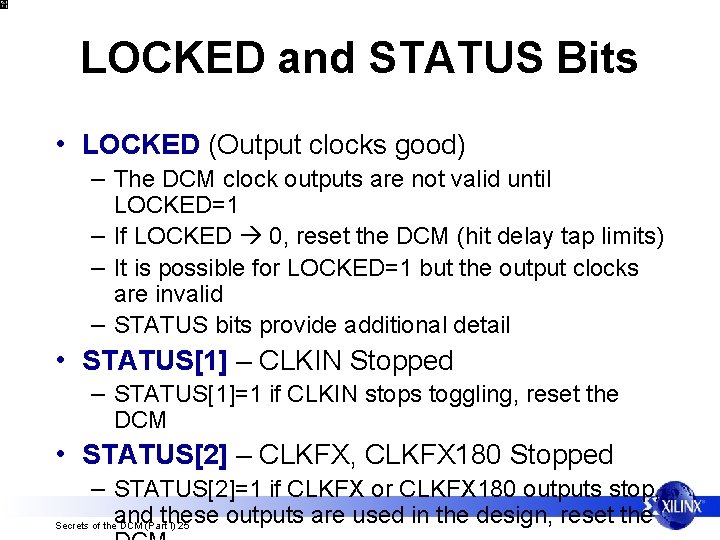
LOCKED and STATUS Bits • LOCKED (Output clocks good) – The DCM clock outputs are not valid until LOCKED=1 – If LOCKED 0, reset the DCM (hit delay tap limits) – It is possible for LOCKED=1 but the output clocks are invalid – STATUS bits provide additional detail • STATUS[1] – CLKIN Stopped – STATUS[1]=1 if CLKIN stops toggling, reset the DCM • STATUS[2] – CLKFX, CLKFX 180 Stopped – STATUS[2]=1 if CLKFX or CLKFX 180 outputs stop, and these outputs are used in the design, reset the Secrets of the DCM (Part I) 25

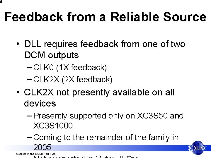
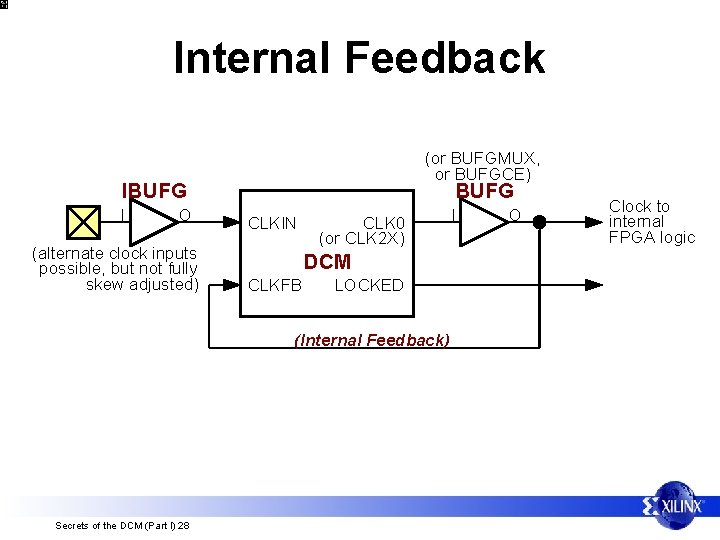
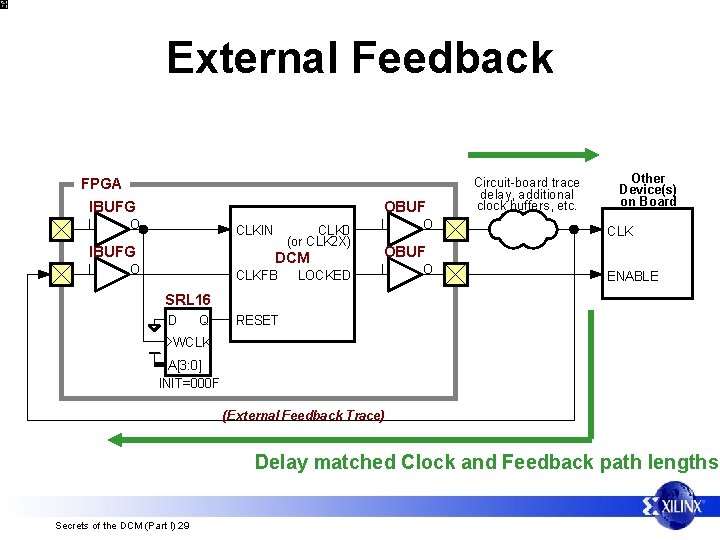
Feedback from a Reliable Source • DLL requires feedback from one of two DCM outputs – CLK 0 (1 X feedback) – CLK 2 X (2 X feedback) • CLK 2 X not presently available on all devices – Presently supported only on XC 3 S 50 and XC 3 S 1000 – Coming to the remainder of the family in 2005 Secrets of the DCM (Part I) 26

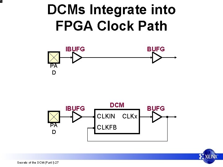
DCMs Integrate into FPGA Clock Path IBUFG PA D IBUFG DCM CLKIN PA D Secrets of the DCM (Part I) 27 CLKFB CLKx BUFG

Internal Feedback (or BUFGMUX, or BUFGCE) IBUFG I O (alternate clock inputs possible, but not fully skew adjusted) BUFG CLKIN CLK 0 (or CLK 2 X) DCM CLKFB LOCKED (Internal Feedback) Secrets of the DCM (Part I) 28 I O Clock to internal FPGA logic

External Feedback FPGA IBUFG I OBUF O CLKIN IBUFG I CLK 0 (or CLK 2 X) DCM O CLKFB LOCKED I O Circuit-board trace delay, additional clock buffers, etc. Other Device(s) on Board CLK OBUF I O ENABLE SRL 16 D Q RESET WCLK A[3: 0] INIT=000 F (External Feedback Trace) Delay matched Clock and Feedback path lengths Secrets of the DCM (Part I) 29

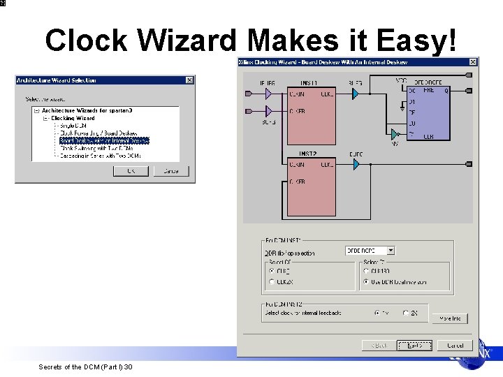
Clock Wizard Makes it Easy! Secrets of the DCM (Part I) 30

Lesson Two Wizard School

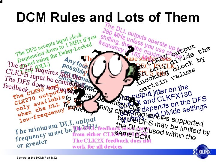
DCM Rules and Lots of Them Th e 280 DLL o MH utpu k c s o u h l o c iftin z unl ts op y t f u i p in MHz d freq g, the ess y erate s t p uen n th ou u up t t e cce n to 1 -Locke a c u e S y s o p w F e y h m is 1 D ies do Dela t p t a e h u x h 6 a i ose de T uenc mum 5 M he A t V g H i by q n The variable phase shifter uses z. LKD v ny f fre ot usi i d ck C PSCLK, The D pos outhe y PSEN, PSINCDEC, are. Ln. Lp r(DLL) r e of t h onl clo s T h CLKFLBoo equires tchan csible. PSDONE, e e ni and STATUS g D u bits n n C a l a o t i n c omi va The DF nput be ccolnocktbhennect M out e c in p n S n t u u e T o d i c o f hte f. em e feedba ta rso globa ts r e reeda h t e ck LK 90 s naontdtresqusaih n o u c l r r n eift m t of p u itte j C p t 0 u t 8 p e t u a 1 u h h o X y e o T F a t l e o b K 0 s h 7 tine in e limi T e and CL ab FS D e h CLK 2 avail LL firse h t t X e F n d e comin o K L d s y d D d s C o q l n g u m u e n n i e e t p g e t o h e y e n d t c s T c cy loohcue n ktpfuret quaenndc Divide when freque ies sup by tuhletiply lowtput M ported DFS m ou L L D t a y be lim zfeedbackhe m u D H L m The DLL must come M i L n 4 i i 2 f ited by u s e saor d The m ncy must be from either CLK 0 w m. CLK 2 X. ithin the e DCM e u q fre The CLK 2 X feedback does not r e t a e r or g work for all devices Secrets of the DCM (Part I) 32

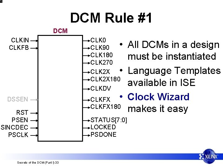
DCM Rule #1 DCM CLKIN CLKFB DSSEN RST PSEN PSINCDEC PSCLK Secrets of the DCM (Part I) 33 CLK 0 CLK 90 CLK 180 CLK 270 CLK 2 X 180 CLKDV • All DCMs in a design must be instantiated • Language Templates available in ISE CLKFX • Clock Wizard CLKFX 180 makes it easy STATUS[7: 0] LOCKED PSDONE

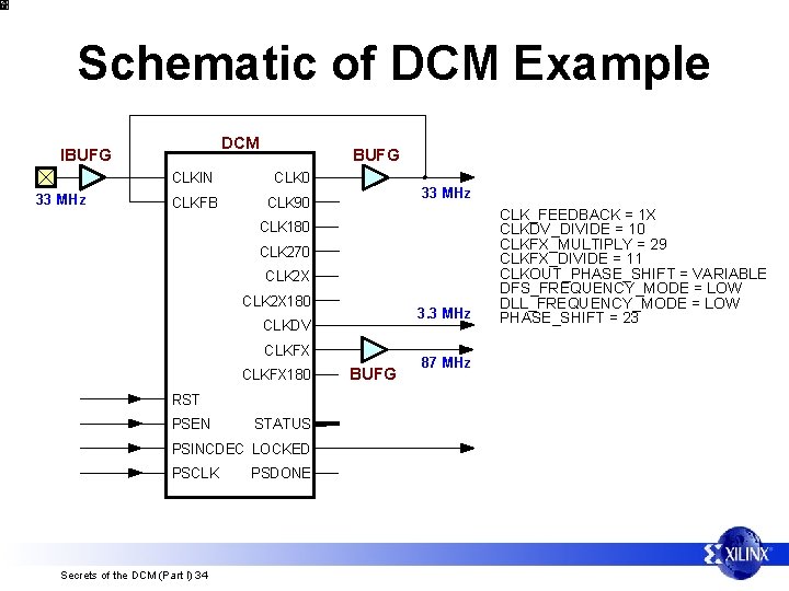
Schematic of DCM Example DCM IBUFG 33 MHz BUFG CLKIN CLK 0 CLKFB CLK 90 33 MHz CLK 180 CLK 270 CLK 2 X 180 3. 3 MHz CLKDV CLKFX 180 RST PSEN STATUS PSINCDEC LOCKED PSCLK Secrets of the DCM (Part I) 34 PSDONE BUFG 87 MHz CLK_FEEDBACK = 1 X CLKDV_DIVIDE = 10 CLKFX_MULTIPLY = 29 CLKFX_DIVIDE = 11 CLKOUT_PHASE_SHIFT = VARIABLE DFS_FREQUENCY_MODE = LOW DLL_FREQUENCY_MODE = LOW PHASE_SHIFT = 23

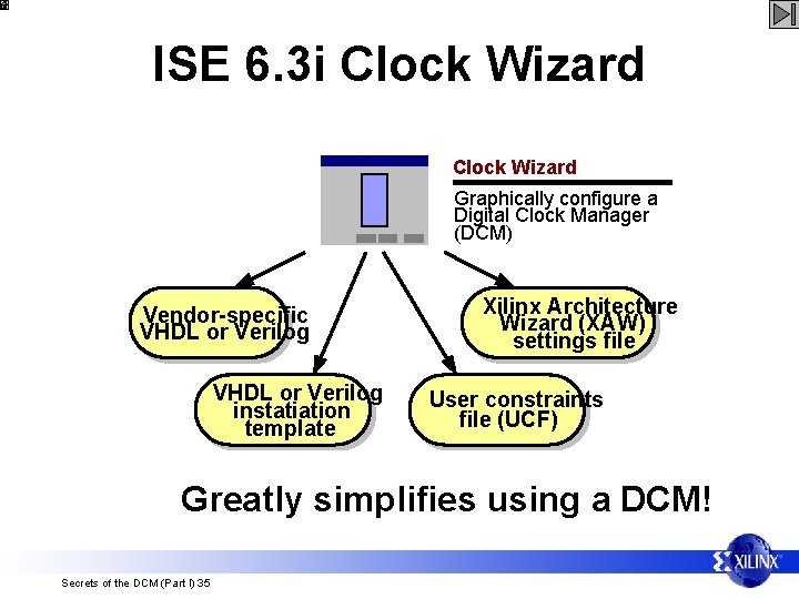
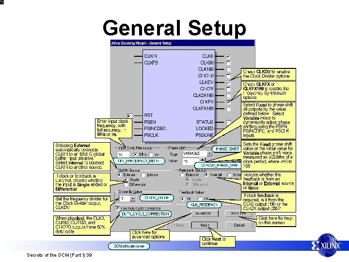
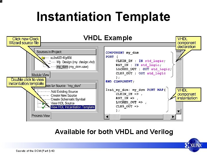
ISE 6. 3 i Clock Wizard Graphically configure a Digital Clock Manager (DCM) Vendor-specific VHDL or Verilog instatiation template Xilinx Architecture Wizard (XAW) settings file User constraints file (UCF) Greatly simplifies using a DCM! Secrets of the DCM (Part I) 35

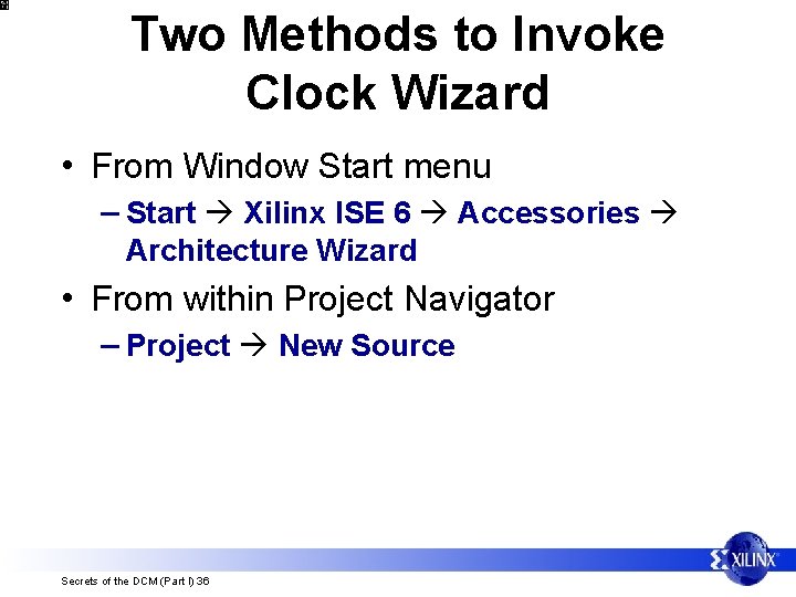
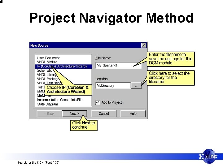
Two Methods to Invoke Clock Wizard • From Window Start menu – Start Xilinx ISE 6 Accessories Architecture Wizard • From within Project Navigator – Project New Source Secrets of the DCM (Part I) 36

Project Navigator Method Secrets of the DCM (Part I) 37

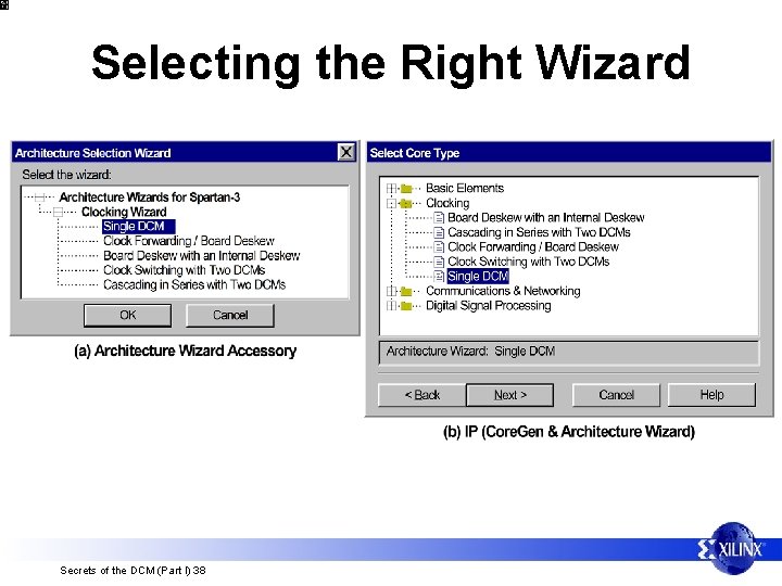
Selecting the Right Wizard Secrets of the DCM (Part I) 38

General Setup Secrets of the DCM (Part I) 39

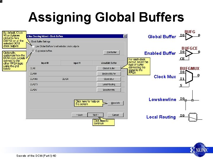
Assigning Global Buffers Global Buffer Enabled Buffer I 0 BUFG O BUFGCE I 0 O CE BUFGMUX I 0 O Clock Mux I 1 S Lowskewline I 0 Local Routing I 0 Secrets of the DCM (Part I) 40

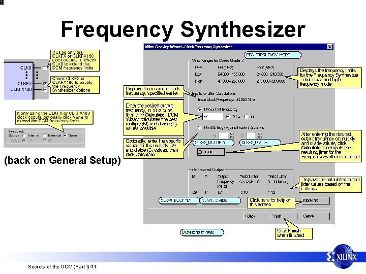
Frequency Synthesizer (back on General Setup) Secrets of the DCM (Part I) 41

Voila! Secrets of the DCM (Part I) 42

Instantiation Template VHDL Example Available for both VHDL and Verilog Secrets of the DCM (Part I) 43

Lesson Three Jitter

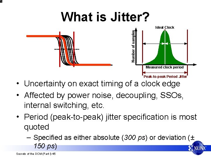
What is Jitter? Number of samples Ideal Clock Measured clock period Peak-to-peak Period Jitter • Uncertainty on exact timing of a clock edge • Affected by power noise, decoupling, SSOs, internal switching, etc. • Period (peak-to-peak) jitter specification is most quoted – Specified as either absolute (300 ps) or deviation (± 150 ps) Secrets of the DCM (Part I) 45

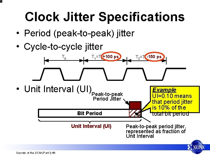
Clock Jitter Specifications • Period (peak-to-peak) jitter • Cycle-to-cycle jitter T 0 T 1=T 0+100 ps • Unit Interval (UI)Peak-to-peak Period Jitter Bit Period Unit Interval (UI) Secrets of the DCM (Part I) 46 T 2=T 1 -150 ps Example UI=0. 10 means that period jitter is 10% of the total bit period Peak-to-peak period jitter, represented as fraction of Unit Interval

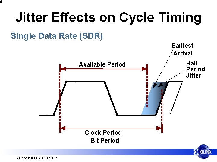
Jitter Effects on Cycle Timing Single Data Rate (SDR) Earliest Arrival Available Period Clock Period Bit Period Secrets of the DCM (Part I) 47 Half Period Jitter

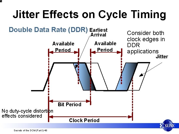
Jitter Effects on Cycle Timing Double Data Rate (DDR) Earliest Arrival Available Period Consider both clock edges in DDR applications Jitter Bit Period No duty-cycle distortion effects considered Secrets of the DCM (Part I) 48 Clock Period

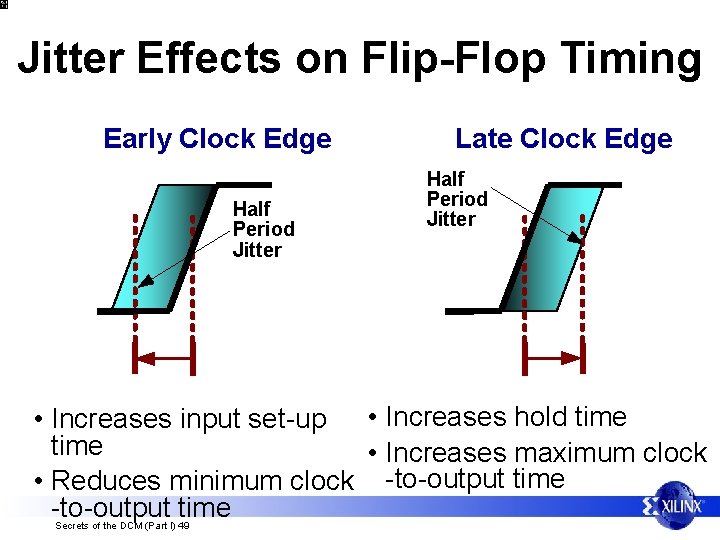
Jitter Effects on Flip-Flop Timing Early Clock Edge Half Period Jitter Late Clock Edge Half Period Jitter • Increases input set-up • Increases hold time • Increases maximum clock • Reduces minimum clock -to-output time Secrets of the DCM (Part I) 49

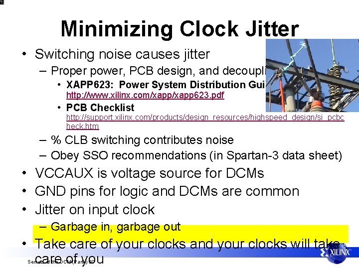
Minimizing Clock Jitter • Switching noise causes jitter – Proper power, PCB design, and decoupling • XAPP 623: Power System Distribution Guidelines http: //www. xilinx. com/xapp 623. pdf • PCB Checklist http: //support. xilinx. com/products/design_resources/highspeed_design/si_pcbc heck. htm – % CLB switching contributes noise – Obey SSO recommendations (in Spartan-3 data sheet) • VCCAUX is voltage source for DCMs • GND pins for logic and DCMs are common • Jitter on input clock – Garbage in, garbage out • Take care of your clocks and your clocks will take care of you Secrets of the DCM (Part I) 50

GOVERNMENT HEALTH WARNING: FAILING TO APPLY XAPP 623 COULD BE HAZARDOUS TO YOUR DCM DESIGN AND YOUR MENTAL HEALTH Secrets of the DCM (Part I) 51

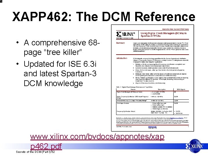
XAPP 462: The DCM Reference • A comprehensive 68 page “tree killer” • Updated for ISE 6. 3 i and latest Spartan-3 DCM knowledge www. xilinx. com/bvdocs/appnotes/xap p 462. pdf Secrets of the DCM (Part I) 52

Second Verse, Same as the First* • If you enjoyed this session, please also attend … Secrets of the DCM Part II * Only a little bit louder and a whole lot worse Secrets of the DCM (Part I) 53

Questions? gpd_apps@xilinx. com Secrets of the DCM (Part I) 54

Please Fill Out and Return the Feedback Forms! • Forms are in the back of your FAE conference book • Please return at back of the room Secrets of the DCM: Part 1 Steve Knapp ü ü ü Secrets of the DCM (Part I) 55 ! u o Y k n a h T

Jump Point • Overview • Lesson 1: Avoid Being Skewed • Lesson 2: Clock Wizard School • Lesson 3: Clock Jitter • Session Evaluation Forms Return to last slide viewe Secrets of the DCM (Part I) 56