
Search for Optimum and Scalable COSMOS Savas Kaya
Search for Optimum and Scalable COSMOS Savas Kaya and Ahmad Al-Ahmadi School of EE&CS Russ College of Eng & Tech e-mail: kaya@ohio. edu © S Kaya IWCE-10, Purdue, Indiana
Outline n Motivation Limitations of Conventional Static CMOS ¨ Technology Base ¨ n n © S Kaya COSMOS Architecture COSMOS Device Operation Scaling & Optimization Conclusions IWCE-10, Purdue, Indiana
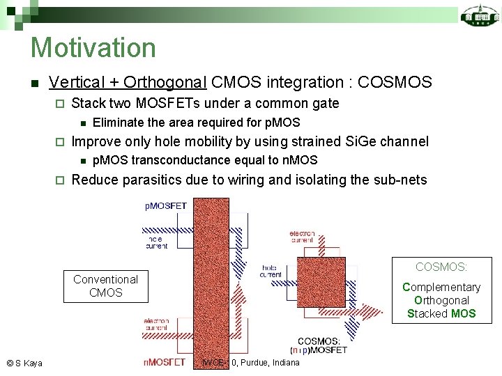
Motivation n Vertical + Orthogonal CMOS integration : COSMOS ¨ Stack two MOSFETs under a common gate n ¨ Improve only hole mobility by using strained Si. Ge channel n ¨ Eliminate the area required for p. MOS transconductance equal to n. MOS Reduce parasitics due to wiring and isolating the sub-nets COSMOS: Conventional CMOS © S Kaya Complementary Orthogonal Stacked MOS IWCE-10, Purdue, Indiana
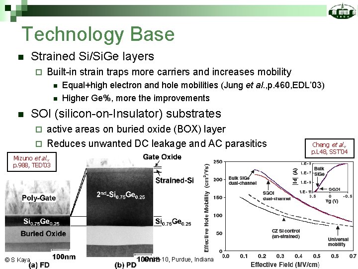
Technology Base n Strained Si/Si. Ge layers ¨ Built-in strain traps more carriers and increases mobility n n n Equal+high electron and hole mobilities (Jung et al. , p. 460, EDL’ 03) Higher Ge%, more the improvements SOI (silicon-on-Insulator) substrates active areas on buried oxide (BOX) layer ¨ Reduces unwanted DC leakage and AC parasitics ¨ Mizuno et al. , p. 988, TED’ 03 © S Kaya IWCE-10, Purdue, Indiana Cheng et al. , p. L 48, SST’ 04
Outline n n Motivation COSMOS Architecture ¨ n n n © S Kaya Layer structure COSMOS Devices Scaling & Optimization Conclusions IWCE-10, Purdue, Indiana
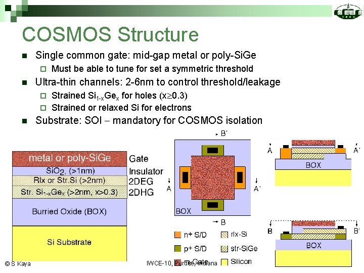
COSMOS Structure n Single common gate: mid-gap metal or poly-Si. Ge ¨ n Must be able to tune for set a symmetric threshold Ultra-thin channels: 2 -6 nm to control threshold/leakage Strained Si 1 -x. Gex for holes (x 0. 3) ¨ Strained or relaxed Si for electrons ¨ n © S Kaya Substrate: SOI mandatory for COSMOS isolation IWCE-10, Purdue, Indiana
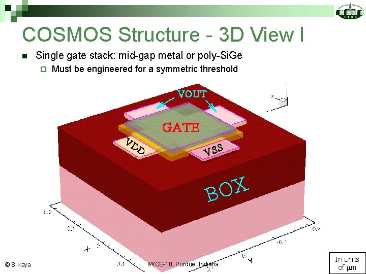
COSMOS Structure - 3 D View I n Single gate stack: mid-gap metal or poly-Si. Ge ¨ © S Kaya Must be engineered for a symmetric threshold IWCE-10, Purdue, Indiana In units of m
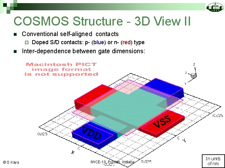
COSMOS Structure - 3 D View II n Conventional self-aligned contacts ¨ n © S Kaya Doped S/D contacts: p- (blue) or n- (red) type Inter-dependence between gate dimensions: IWCE-10, Purdue, Indiana In units of nm
Outline n n n Motivation COSMOS Architecture COSMOS Devices Operation ¨ I-V Characteristics ¨ Logic Gates ¨ n n © S Kaya Scaling & Optimization Conclusions IWCE-10, Purdue, Indiana
COSMOS Gate Control n A single gate to control both channels ¨ High-mobility strained Si 1 -x. Gex (x 0. 3) buried hole channel n n ¨ Electrons are in a surface channel n ¨ © S Kaya High Ge% eliminates parallel conduction and improves mobility Lowers the threshold voltage VT May be relaxed or strained Requires fines tuning for symmetric operation IWCE-10, Purdue, Indiana
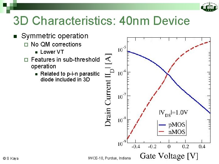
3 D Characteristics: 40 nm Device n Symmetric operation ¨ No QM corrections n ¨ Features in sub-threshold operation n © S Kaya Lower VT Related to p-i-n parasitic diode included in 3 D IWCE-10, Purdue, Indiana
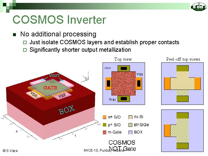
COSMOS Inverter n No additional processing Just isolate COSMOS layers and establish proper contacts ¨ Significantly shorter output metallization ¨ Top view © S Kaya IWCE-10, Purdue, Indiana Peel-off top views
3 D TCAD Verification n Inverter operation verified in 3 D 40 nm COSMOS NOT gate driving CL=1 f. F load © S Kaya IWCE-10, Purdue, Indiana
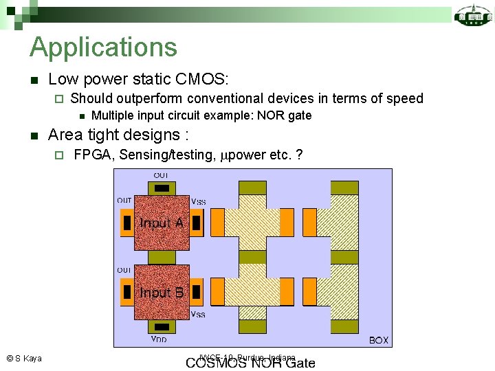
Applications n Low power static CMOS: ¨ Should outperform conventional devices in terms of speed n n Area tight designs : ¨ © S Kaya Multiple input circuit example: NOR gate FPGA, Sensing/testing, power etc. ? IWCE-10, Purdue, Indiana
Outline n n Motivation COSMOS Architecture COSMOS Devices Scaling & Optimization Vertical Scaling ¨ Lateral Scaling ¨ Voltage Scaling ¨ n © S Kaya Conclusions IWCE-10, Purdue, Indiana
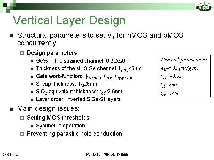
Vertical Layer Design n Structural parameters to set VT for n. MOS and p. MOS concurrently ¨ Design parameters: n n n n Ge% in the strained channel: 0. 3 x 0. 7 Thickness of the str. Si. Ge channel: t. Si. Ge 5 nm Gate work-function: n-poly. Si MS p-poly. Si Si cap thickness: t. Si 5 nm Si. O 2 equivalent thickness: tox 2. 5 nm Layer order: inverted Si. Ge/Si layers Main design issues: ¨ Setting MOS thresholds n ¨ © S Kaya Symmetric operation Preventing parasitic hole conduction IWCE-10, Purdue, Indiana Nominal parameters: MS= Si (midgap) t. Si. Ge=3 nm t. Si=2 nm tox=1 nm
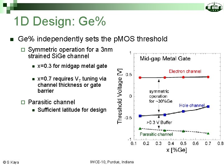
1 D Design: Ge% n Ge% independently sets the p. MOS threshold ¨ ¨ Symmetric operation for a 3 nm strained Si. Ge channel n x=0. 3 for midgap metal gate n x=0. 7 requires VT tuning via channel thickness or gate barrier Parasitic channel n © S Kaya Sufficient latitude for design IWCE-10, Purdue, Indiana
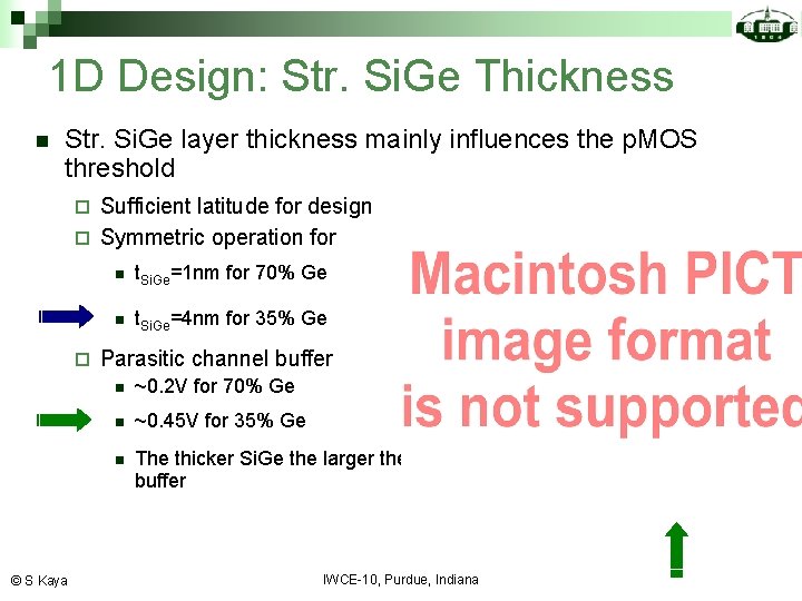
1 D Design: Str. Si. Ge Thickness n Str. Si. Ge layer thickness mainly influences the p. MOS threshold Sufficient latitude for design ¨ Symmetric operation for ¨ ¨ © S Kaya n t. Si. Ge=1 nm for 70% Ge n t. Si. Ge=4 nm for 35% Ge Parasitic channel buffer n ~0. 2 V for 70% Ge n ~0. 45 V for 35% Ge n The thicker Si. Ge the larger the buffer IWCE-10, Purdue, Indiana
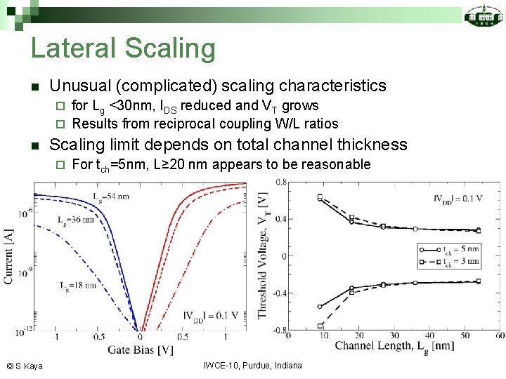
Lateral Scaling n Unusual (complicated) scaling characteristics for Lg <30 nm, IDS reduced and VT grows ¨ Results from reciprocal coupling W/L ratios ¨ n Scaling limit depends on total channel thickness ¨ © S Kaya For tch=5 nm, L≥ 20 nm appears to be reasonable IWCE-10, Purdue, Indiana
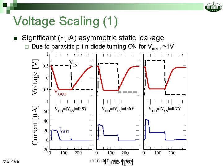
Voltage Scaling (1) n Significant (~ A) asymmetric static leakage ¨ © S Kaya Due to parasitic p-i-n diode turning ON for Vdrive >1 V IWCE-10, Purdue, Indiana
Voltage Scaling (2) n Suitable for low-power applications ¨ n Limited by static leakage and noise margin Figures of merit for 36 nm COSMOS @ CL=1 f. F , |VDD|= 0. 5 V td ~150 ps ¨ No loss of NM ¨ Istatic ~ 10 n. A ¨ © S Kaya IWCE-10, Purdue, Indiana
Summary & Conclusions n Described a novel CMOS architecture COSMOS Single gate symmetric CMOS ¨ Suitable for low-power & area tight applications ¨ n n Used 3 D simulations to verify operation Identified performance figures and applications ± 0. 5 V bipolar digital operation ¨ ~100 ns delays => GHz digital operation ¨ Limited due to static leakage ¨ n Different scaling behaviour VT grows at smaller gate lengths ¨ 20 nm gate length is achievable ¨ Concerns for end-of-roadmap (10 nm) requirements. ¨ © S Kaya IWCE-10, Purdue, Indiana
- Slides: 22