Schematics Layout First contact with Cadence icfb PreSteps

Schematics & Layout First contact with Cadence icfb

Pre-Steps for windows user: • 1. Get an account on the Cadence server. • 2. Login into the server with ssh. – ssh 192. 168. 1. 2 • 3. Start the VNC server for yourself. – vncserver –depth 24 –geometry 1024 x 768 – Set a your vncserver password. – Remember your password and port number • 4. Run VNC viewer – Server: 192. 168. 1. 2: 5901 (w/ your port)

Pre-Steps for windows user: • You need to re-do step 2 & 3 only after – you killed the vncserver – Or, a reboot of the server. • If you are in a network outside our lab, please contact us to get the server ip and port.
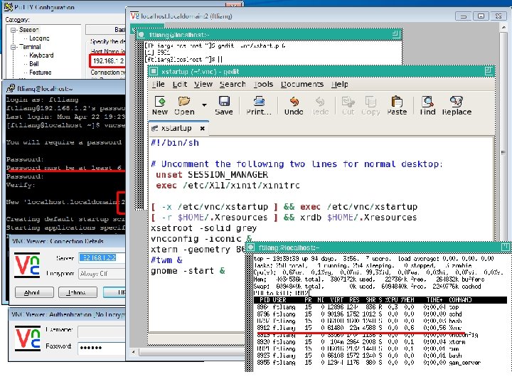

Pre-Steps for Linux & Mac user: • 1. Get an account on the Cadence server. • 2. Login into the server with ssh in any GUI. – ssh -X 192. 168. 1. 2 • You are ready to configure and run Cadence.

First contact • Make a directory where you want to begin and save your design. – mkdir mydesign • Change to the directory. – cd mydesign • Run cadence – – – csh source (something? ) virtuoso & (virtuoso -64 if you want to run 64 bit version) Read and close the “What’s new” window. Ready to work?

First contact: Ready to work? • For design safety: – You may want to mount a net drive as your design folder • Configure the PDK. – The PDK has been install on the server – You need configure your environment to invoke it.

Configure / invoke the PDK • Copy and rename cdsinit to your home folder – mv cdsinit • Copy cshrc_wrk. Dir and cds. lib to your design folder • cd to your design folder and run – csh – source cshrc_wrk. Dir – virtuoso & • You may need to update cshrc_wrk. Dir if you change a PDK.

This log window is useful. You will know when to read it carefully. Tools->Library Manager… is another important window. We face to it almost everyday. You can manage (create / add/ remove) your library in this window. Try to know more about it. Now, this is a default library list.

Tools & Software for windows user • Putty. exe -- ssh tools. • vnc-4_1_3 -x 86_win 32_viewer. exe -- vncviewer • X-windows directly on your windows desktop. – In Pu. TTY: Configuration->Connection->SSH-> X 11 ->Check Enable X 11 forwarding – Install Xming-6 -9 -0 -31 -setup. exe, Xming-mesa-6 -9 -0 -31 setup. exe, Xming-fonts-7 -5 -0 -34 -setup. exe – Start Xming – Start icfb from your ssh command line. • Win. SCP – A file transfer between your PC and system server

To our business – schematic and layout

Design Flow

Create your library • In Library manager: – File->New->Library – Name->OK • Technology File for New … ->Attach to an existing techfile->OK • Attach Design Library to Technology File smic 13 mmrf_1233 ->OK
 • In Library manager: – Select “mystudy” – File->New->Cell View")
Create your cell (1) • In Library manager: – Select “mystudy” – File->New->Cell View – Name -> OK • In Virtuoso? Schematic Editing: mystudy… – Creat->Instance…(i) – Add Instance: Browse – Library: smic 13 mmrf_1233, Cell: n 12, View: symbol ->Close
 • • • Adjust parameters as needed. Hide-> Left click")
Create your cell (2) • • • Adjust parameters as needed. Hide-> Left click to place the component ESC key to finish the placement. Then, add a p 12. Add->Pin… p – A: input – Y: output – vcc, gnd: input. Output
 • Add->Wire (narrow) w – Click and connect the components.")
Create your cell (3) • Add->Wire (narrow) w – Click and connect the components. • Save(the left check icon) • The warnings are highlighted. • Modify and save again. • (No 4 wires junction, please)

Create a symbol for a cell view • In Schematic Editing window, – Design->Create Cellview->From Cellview – OK • Symbol Generation Options – Adjust the pin location – OK • In symbol Editing: – Change the shape with Add->Shape – Save

ACHTUNG!!!!WARNING!!! • Please note that usually according to normal design flow you would move onto to schematic simulation to verify that your design is correct( i. e. . Transistor sizing etc). • However, in an effort to get the student more familiar with the tools we will continue straight to layout.
 • In Library Manger window, – File->New->Library->Cell View… – Tools:")
Create your layout (1) • In Library Manger window, – File->New->Library->Cell View… – Tools: layout – OK • LSW window show the layer and colors • In Layout Editing windows: – Creat->Instance i – Browse and fine layout of n 12 and p 12
 • Press “shift+f” to switch to the detail view •")
Create your layout (2) • Press “shift+f” to switch to the detail view • Press “ctrl+f” to switch back • Click a component to select it. • Then press “q” to edit properties.
 • In Edit Instance Properties windows, – Parameter->Bodytie Type: Integrated")
Create your layout (3) • In Edit Instance Properties windows, – Parameter->Bodytie Type: Integrated ->Left Tap – OK • In LSW – Select GT drw • In Layout Editing: – Create Path p to connect poly. • Then, connect Y w/ MET 1 drw.
 • • Add pin labels for each pin labels must")
Create your layout (4) • • Add pin labels for each pin labels must in metal tex layers for smic 130 LSW->M 1 TXT drw In Layout Editing: – Create Label l (lower-case L) – Place on metal • Then, – Y, vcc, gnd
 • In Layout Editing: – Calibre->Run DRC • Calibre Interactive")
Design Rules Checks (DRC) • In Layout Editing: – Calibre->Run DRC • Calibre Interactive -DRC – Cancel the “Load Runset File” – Rules->Calibre-DRC Rules File->… • /eda/smic 13 mmrf_1233…. v 2. 6/Calibr/DRC/Smic. DR 19… 1215 33. drc – Rules->Calibre-DRC Run Directory->… • /home/ftliang/mydesign/drc – Run DRC – Only Metal Density check can be failed during the components design.
 • In Layout Editing: – Calibre->Run LVS • Calibre Interactive")
Layout Versus Schematic (LVS) • In Layout Editing: – Calibre->Run LVS • Calibre Interactive –LVS – Cancel – Rules->Calibre-LVS Rules File->… • /eda/smic 13 mmrf…. v 2. 6/Calibre/LVS/Smic. SPM 7…V 2. 6_ 2 P. lvs_XRC – Rules->Calibre-DRC Run Directory->… • /home/ftliang/mydesign/lvs – Inputs->Netlist->Check Export from schematic …

Thanks & Please re-try some yourself.

Schematic simulation DC simulation of a single transistor

Clarifications: n. MOS vs p. MOS n. MOS with p-substrate, p. MOS w/ n-well or n-substrate

Clarifications: n. MOS vs. p. MOS Current arrow also on the source, and current direction decides the type of MOS Be aware of the difference between VDS and VSD

Outlines • What is a IV curve of a n. MOS or p. MOS? • Simulation test bench

What is a IV curve?
")
Simulation test bench 1 • • • Start virtuoso & New cell view (schematic) Add n. MOS. Add gnd, vdc x 2 from analog. Lib Connect them

Simulation test bench 2 • Change parameters of V 0, V 1 with key q • V 0 – DC voltage: Vds • V 1 – DC voltage: Vgs • Check and Save
 • In")
Simulation Settings 1 • In Virtuoso Schematic window – Tools->Analog Environment (ADE) • In ADE window – Setup->Model Libraries & Temperature (at least) – Variables->Copy From Cellview • Edit->Vgs=0, Vds=3. 3 – Analyses->Choose

DC Simulation Settings • Choosing Analyses – dc – Component Parameter – Select Component->V 0 ->vdc->OK – Sweep Range->Start-Stop->0~1. 2 – OK • ADE – Outputs->To Be Plotted->Pick up the drain of n. MOD

Setting Vgs via Parametric Analysis • ADE->Tools->Parametric Analysis… • Sweep->Parametric Set – Variable Name: Vgs – Value List: – 0. 5 1 1. 5 2 2. 5 3 3. 3 – Check Select – Analysis->Start – Nothing output? – You should “Netlist and run” first.

You should know • • • How to plot schematic How to plot simulation graph output How to save simulation setting How to adjust the graphs. How to measure something on graphs. How to calculate values in ADE and calculator.
 • Sweep->Vds")
Now swith Vgs and Vds • dc->V 1 (Vgs) • Sweep->Vds

Try p. MOS yourselves

Thanks & Please re-try some yourself.

Post-layout simulation Transient simulations of a invertor Pre- and Post-layout

Outlines • CMOS fabrication • Invertor – Schematic – Layout • Transient simulations – Pre-layout simulation – PEX, parameter extraction – Post-layout simulation -- F. Liang @USTC, 2013

CMOS fabrication Post-layout simulation -- F. Liang @USTC, 2013

Invertor • You should have your schematic and layout from Lab 1. – If you didn’t, you are fine to drop this course. • No matter your layout is good or not, it should pass the DRC and LVS. Post-layout simulation -- F. Liang @USTC, 2013

Transient simulations • Test bench – The configuration of vpulse – Why I used three invertors? • ADE – Variables->Copy From. Cellview – Analyses->Choose->tran->stop time ->conservative (What is the difference? ) – Output->To Be Plotted – Netlist and Run Post-layout simulation -- F. Liang @USTC, 2013

PEX, parameter extraction • Layout->Calibre->Run PEX – Ruels: /eda/smic 13 mmrf…. v 2. 6/Calibre/LVS/Smic. S PM 7…V 2. 6_2 P. lvs_XRC – Inputs: Netlist->Export from schematic viewer – Outputs: Netlist->Format: CALIBREVIEW, Use Names From: SCHEMATIC – Run PEX (You may get errors, let’s talk. ) – Calibre View Setup window pop up. • Reset Properties: m=1 ng=1 mult=1 • OK • Map calibre device Post-layout simulation -- F. Liang @USTC, 2013

Post-layout simulation • In your test bench cell – File->New->Cell View->Type: config. • Configuration – View: Schematic – Use Template… – spectre – right-click on “inverter” ->Set Cell View->calibre – Save and Close • Re-open config View – ADE Post-layout simulation -- F. Liang @USTC, 2013

Thanks & Please re-try some yourself.

Ocean scripts & misc. Run group of simulations in command line.

Outlines • Misc. – Structure of your design folders – cds. lib – Copy or backup your real design • Ocean script – What is ? – Where to begin with? – Customisation Ocean scripts -- F. Liang @USTC, 2013

Structure of your design folders Ocean scripts -- F. Liang @USTC, 2013

cds. lib • -- 行注�符 • INCLUDE /pdk/chrt 35/cds. lib • DEFINE mystudy /home/ftliang/mydesign/mystudy • In /pdk/chrt 35/cds. lib – $CDSHOME/share/cdssetup/df. II/cds. lib – DEFINE chrt 35 dg_Si. Ge. /chrt 35 dg_Si. Ge Ocean scripts -- F. Liang @USTC, 2013

Copy or backup your real design • Backup: archive all your design folder. – For whole project backup, you may also backup the related pdk library. • Restore: – Modify the cds. lib DEFINE line • In virtuoso, when you make a copy, it is usually not a full backup. – Especially, it is a top level schematic or layout. Ocean scripts -- F. Liang @USTC, 2013

Ocean scripts • ADE->Session->Save Ocean Script… • Edit the script as necessary. • In command line – ocean – load “xxx. ocn” Ocean scripts -- F. Liang @USTC, 2013

Thanks & Please re-try some yourself.
- Slides: 54