
Scanning Electron Microscopy What is an SEM What








- Slides: 26
Scanning Electron Microscopy
What is an SEM?
What is an SEM? • A Scanning Electron Microscope is an instrument that investigates the surfaces of solid samples by using a beam of electrons in a vacuum.
What is an SEM? • A Scanning Electron Microscope is an instrument that investigates the surfaces of solid samples by using a beam of electrons in a vacuum. • The image is generated by the secondary emissions from the sample.
Advantages of using an SEM instead of a light microscope
Advantages of using an SEM instead of a light microscope • Imaging – high resolution (because of short wavelength) - >1. 4 nm
Advantages of using an SEM instead of a light microscope • Imaging – high resolution (because of short wavelength) - >1. 4 nm – Secondary electron imaging for topology
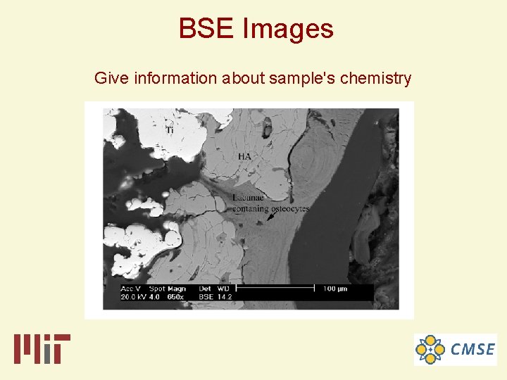
Advantages of using an SEM instead of a light microscope • Imaging – high resolution (because of short wavelength) - >1. 4 nm – Secondary electron imaging for topology – Backscatter electron imaging for chemistry
Advantages of using an SEM instead of a light microscope • Imaging – high resolution (because of short wavelength) - >1. 4 nm – Secondary electron imaging for topology – Backscatter electron imaging for chemistry – High depth of field
Advantages of using an SEM instead of a light microscope • Imaging – high resolution (because of short wavelength) - >1. 4 nm – Secondary electron imaging for topology – Backscatter electron imaging for chemistry – High depth of field • Elemental Analysis – EDXS (Energy-dispersive X-ray analysis)
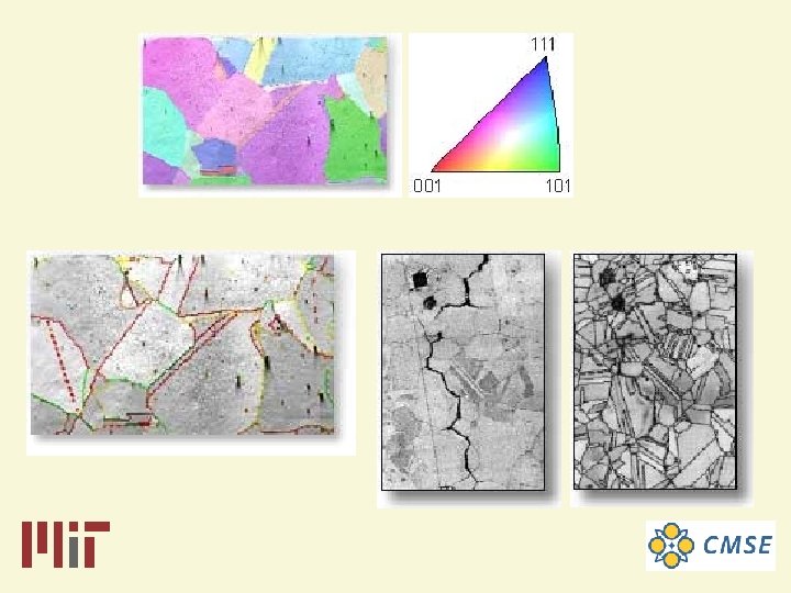
Advantages of using an SEM instead of a light microscope • Imaging – high resolution (because of short wavelength) - >1. 4 nm – Secondary electron imaging for topology – Backscatter electron imaging for chemistry – High depth of field • Elemental Analysis – EDXS (Energy-dispersive X-ray analysis) • Structural Analysis – EBSD (Electron Back-scatter Diffraction analysis)
Advantages of using an SEM instead of a light microscope • Imaging – high resolution (because of short wavelength) - >1. 4 nm – Secondary electron imaging for topology – Backscatter electron imaging for chemistry – High depth of field • Elemental Analysis – EDXS (Energy-dispersive X-ray analysis) • Structural Analysis – EBSD (Electron Back-scatter Diffraction analysis) • Ease of sample preparation since most SEMs only require the sample to be conductive.
Sample Constraints
Sample Constraints • Must fit in chamber (!)
Sample Constraints • Must fit in chamber • Must be compatible with vacuum (even for ESEM samples)
Sample Constraints • Must fit in chamber • Must be compatible with vacuum (even for ESEM samples) • Must have conductive surface (not necessary for ESEM samples)
JEOL 5910 General-Purpose SEM
FEI XL 30 FEG-ESEM
JEOL 6320 High-resolution SEM
Secondary Electron Images Give information about sample's topography
BSE Images Give information about sample's chemistry
EDS Spectra Give information about sample's composition
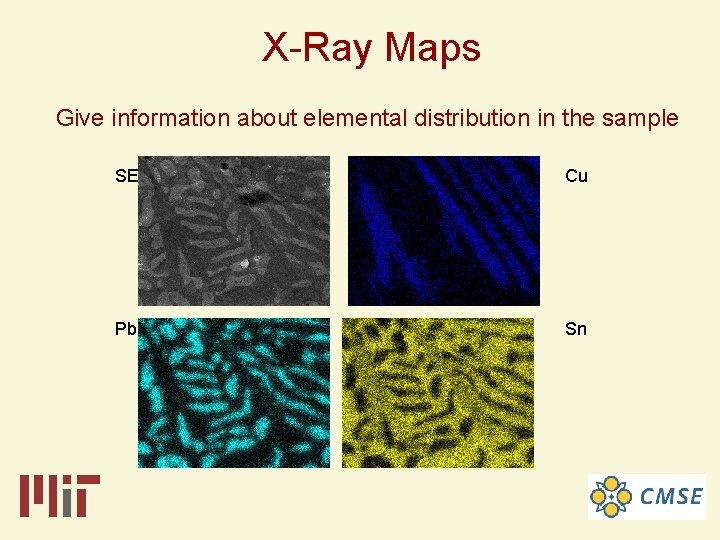
X-Ray Maps Give information about elemental distribution in the sample SE Cu Pb Sn
Electron beam strikes a crystalline material tilted at 70° Backscatter patterns composed of intersecting bands Indexable patterns
Center for Materials Science and Engineering Electron Microscopy SEF Location: 13 -1012 Normal Working Hours: 8: 30 am – 4: 45 pm on M-F 24 hr accessible for evening/weekend users (not for undergraduates) Staff: Dr. Anthony (Tony) Garratt-Reed (TEM, STEM) Dr. Yong Zhang (TEM, STEM) Mr. Patrick Boisvert (SEM, Microtome)