Scanning Electron Microscopy SEM MENA 3100 Outline What

- Slides: 44

Scanning Electron Microscopy (SEM) MENA 3100

Outline • • What can we use a SEM for? How do we get an image? Electron beam-sample interactions Signals that can be used to characterize the microstructure – Secondary electrons – Backscattered electrons – X-rays • Components of the SEM • Some comments on resolution • Summary MENA 3100

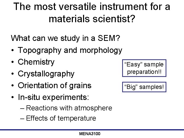
The most versatile instrument for a materials scientist? What can we study in a SEM? • Topography and morphology • Chemistry “Easy” sample preparation!! • Crystallography • Orientation of grains “Big” samples! • In-situ experiments: – Reactions with atmosphere – Effects of temperature MENA 3100

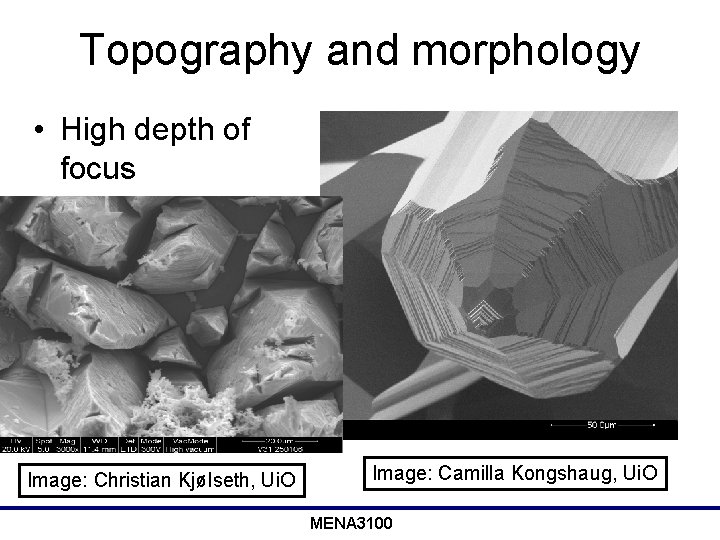
Topography and morphology • High depth of focus Image: Christian Kjølseth, Ui. O Image: Camilla Kongshaug, Ui. O MENA 3100

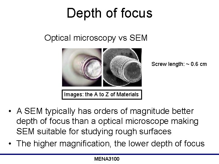
Depth of focus Optical microscopy vs SEM Screw length: ~ 0. 6 cm Images: the A to Z of Materials • A SEM typically has orders of magnitude better depth of focus than a optical microscope making SEM suitable for studying rough surfaces • The higher magnification, the lower depth of focus MENA 3100

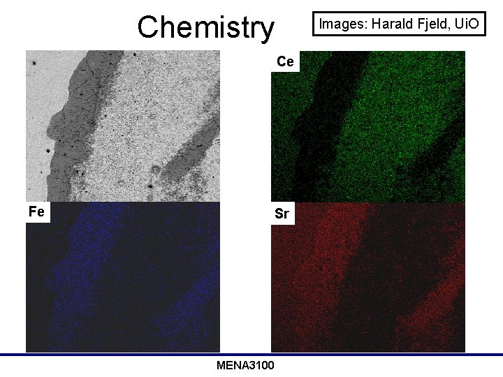
Chemistry Images: Harald Fjeld, Ui. O Ce Fe Sr MENA 3100

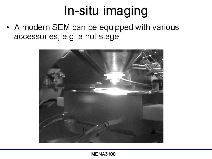
In-situ imaging • A modern SEM can be equipped with various accessories, e. g. a hot stage MENA 3100

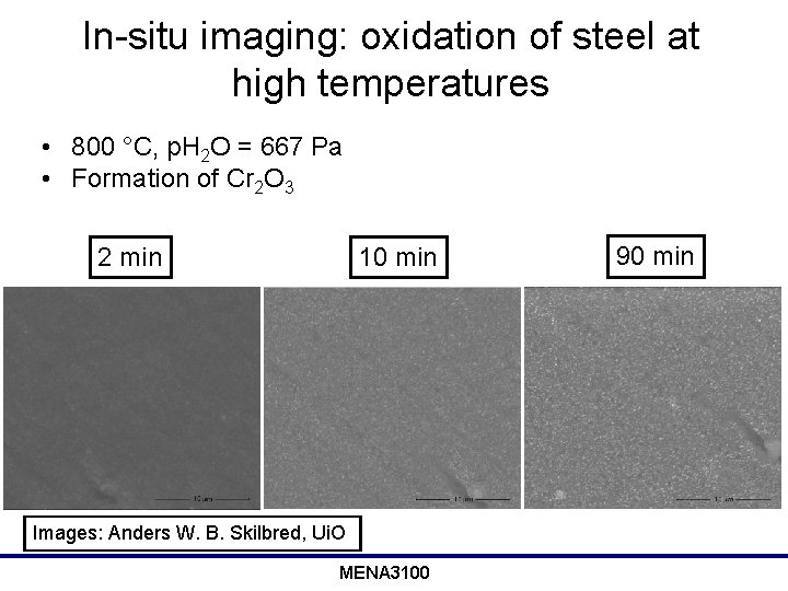
In-situ imaging: oxidation of steel at high temperatures • 800 °C, p. H 2 O = 667 Pa • Formation of Cr 2 O 3 2 min 10 min Images: Anders W. B. Skilbred, Ui. O MENA 3100 90 min

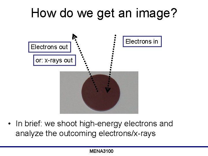
How do we get an image? Electrons in Electrons out or: x-rays out • In brief: we shoot high-energy electrons and analyze the outcoming electrons/x-rays MENA 3100

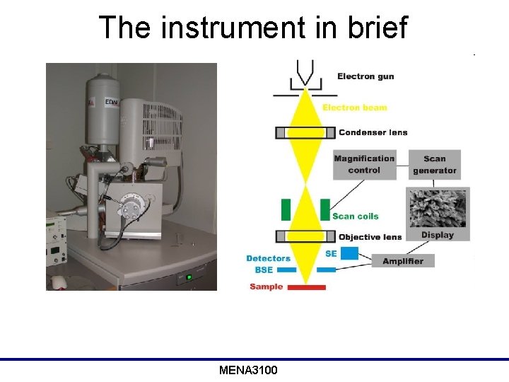
The instrument in brief MENA 3100

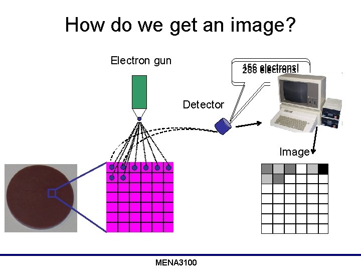
How do we get an image? Electron gun 156 288 electrons! Detector Image MENA 3100

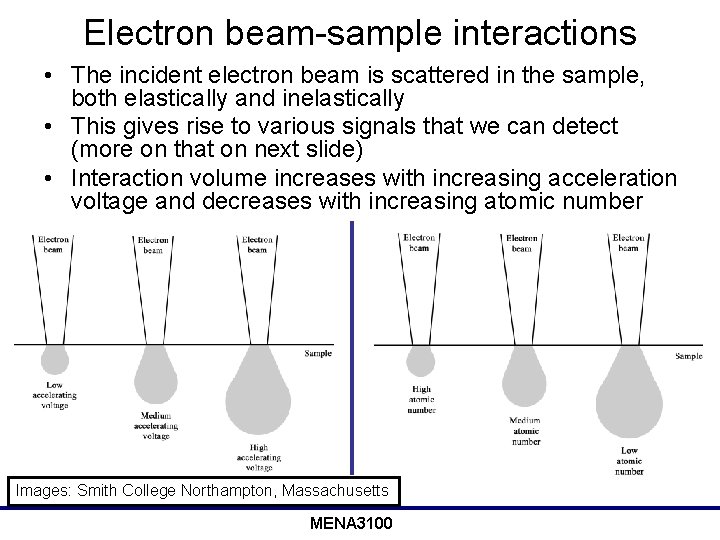
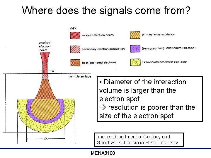
Electron beam-sample interactions • The incident electron beam is scattered in the sample, both elastically and inelastically • This gives rise to various signals that we can detect (more on that on next slide) • Interaction volume increases with increasing acceleration voltage and decreases with increasing atomic number Images: Smith College Northampton, Massachusetts MENA 3100

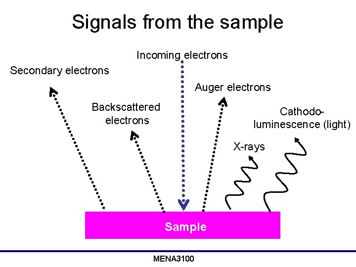
Signals from the sample Incoming electrons Secondary electrons Auger electrons Backscattered electrons Cathodoluminescence (light) X-rays Sample MENA 3100

Image: see the text book, page 281. MENA 3100

Where does the signals come from? • Diameter of the interaction volume is larger than the electron spot resolution is poorer than the size of the electron spot Image: Department of Geology and Geophysics, Louisiana State University MENA 3100

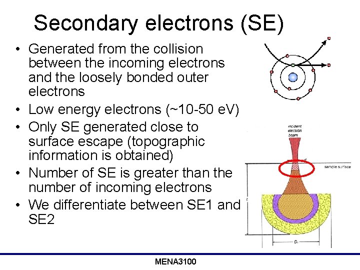
Secondary electrons (SE) • Generated from the collision between the incoming electrons and the loosely bonded outer electrons • Low energy electrons (~10 -50 e. V) • Only SE generated close to surface escape (topographic information is obtained) • Number of SE is greater than the number of incoming electrons • We differentiate between SE 1 and SE 2 MENA 3100

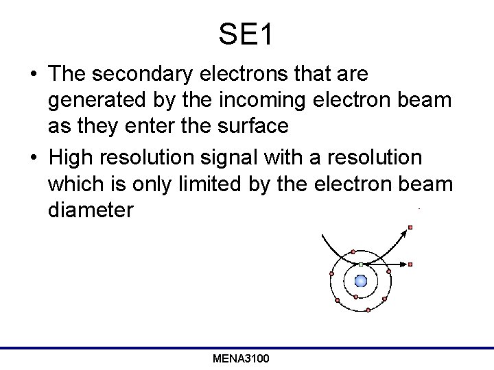
SE 1 • The secondary electrons that are generated by the incoming electron beam as they enter the surface • High resolution signal with a resolution which is only limited by the electron beam diameter MENA 3100

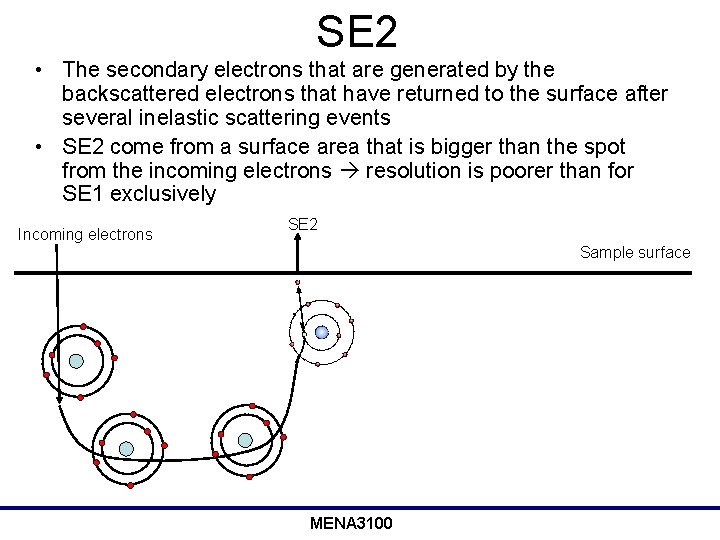
SE 2 • The secondary electrons that are generated by the backscattered electrons that have returned to the surface after several inelastic scattering events • SE 2 come from a surface area that is bigger than the spot from the incoming electrons resolution is poorer than for SE 1 exclusively Incoming electrons SE 2 Sample surface MENA 3100

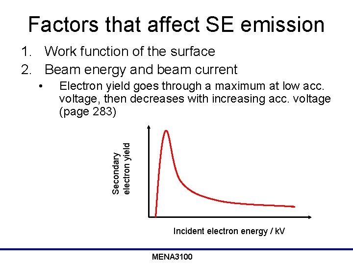
Factors that affect SE emission 1. Work function of the surface 2. Beam energy and beam current Electron yield goes through a maximum at low acc. voltage, then decreases with increasing acc. voltage (page 283) Secondary electron yield • Incident electron energy / k. V MENA 3100

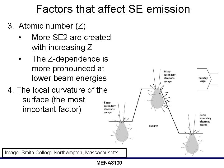
Factors that affect SE emission 3. Atomic number (Z) • More SE 2 are created with increasing Z • The Z-dependence is more pronounced at lower beam energies 4. The local curvature of the surface (the most important factor) Image: Smith College Northampton, Massachusetts MENA 3100

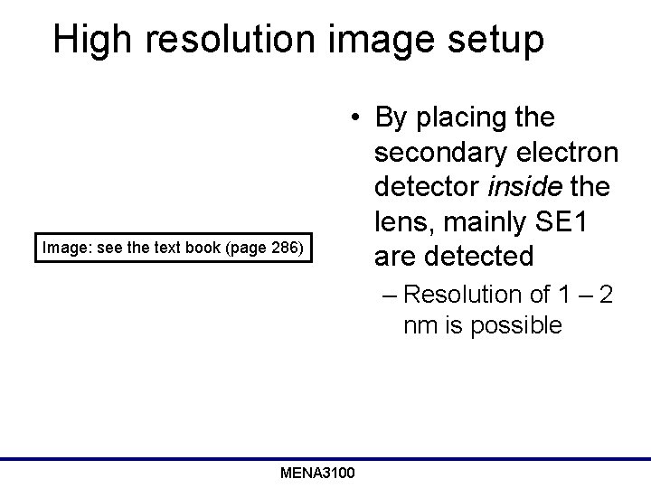
High resolution image setup Image: see the text book (page 286) • By placing the secondary electron detector inside the lens, mainly SE 1 are detected – Resolution of 1 – 2 nm is possible MENA 3100

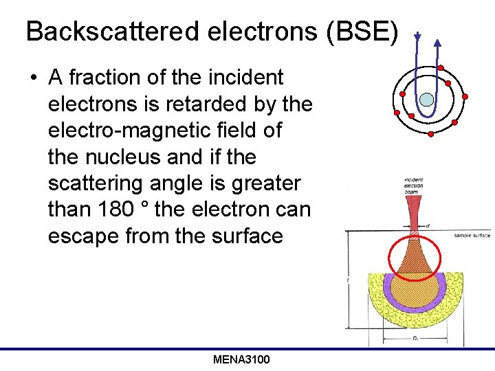
Backscattered electrons (BSE) • A fraction of the incident electrons is retarded by the electro-magnetic field of the nucleus and if the scattering angle is greater than 180 ° the electron can escape from the surface MENA 3100

Backscattered electrons (BSE) • High energy electrons (elastic scattering) • Fewer BSE than SE • We differentiate between BSE 1 and BSE 2 Image: See the text book, page 281. MENA 3100

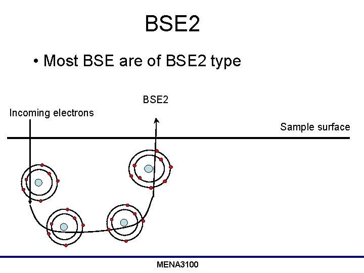
BSE 2 • Most BSE are of BSE 2 type BSE 2 Incoming electrons Sample surface MENA 3100

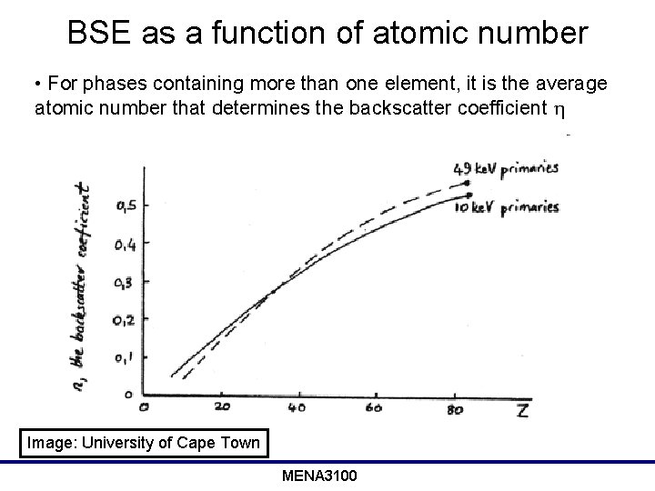
BSE as a function of atomic number • For phases containing more than one element, it is the average atomic number that determines the backscatter coefficient h Image: University of Cape Town MENA 3100

Factors that affect BSE emission • Direction of the irritated surface – more electrons will hit the BSE detector when the surface is aligned towards the BSE detector • Average atomic number • When you want to study differences in atomic numbers the sample should be as levelled as possible (sample preparation is an issue!) MENA 3100

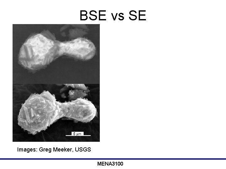
BSE vs SE Images: Greg Meeker, USGS MENA 3100

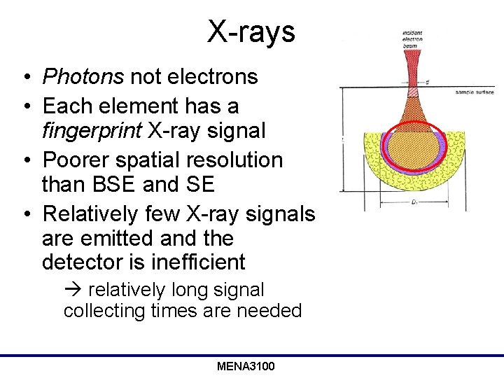
X-rays • Photons not electrons • Each element has a fingerprint X-ray signal • Poorer spatial resolution than BSE and SE • Relatively few X-ray signals are emitted and the detector is inefficient relatively long signal collecting times are needed MENA 3100

X-rays • Most common spectrometer: EDS (energydispersive spectrometer) • Signal overlap can be a problem • We can analyze our sample in different modes – spot analysis – line scan – chemical concentration map (elemental mapping) MENA 3100

Considerations when using EDS • Dead time – some twenty-thirty percent is ok • Statistics – Signal-to-noise ratio • Drift in electron beam with time • Build-up of a carbonaceous contamination film after extended periods of electron probe irradiation MENA 3100

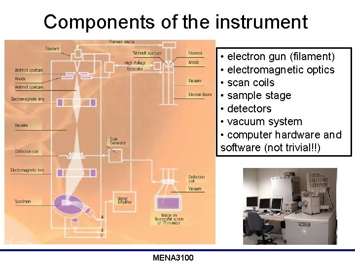
Components of the instrument • electron gun (filament) • electromagnetic optics • scan coils • sample stage • detectors • vacuum system • computer hardware and software (not trivial!!) MENA 3100

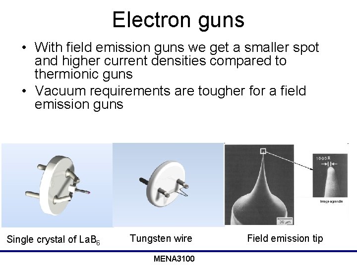
Electron guns • We want many electrons per time unit per area (high current density) and as small electron spot as possible • Traditional guns: thermionic electron gun (electrons are emitted when a solid is heated) – W-wire, La. B 6 -crystal • Modern: field emission guns (FEG) (cold guns, a strong electric field is used to extract electrons) – Single crystal of W, etched to a thin tip MENA 3100

Electron guns • With field emission guns we get a smaller spot and higher current densities compared to thermionic guns • Vacuum requirements are tougher for a field emission guns Single crystal of La. B 6 Tungsten wire MENA 3100 Field emission tip

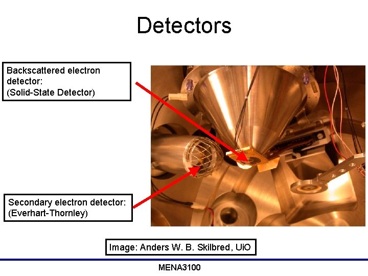
Detectors Backscattered electron detector: (Solid-State Detector) Secondary electron detector: (Everhart-Thornley) Image: Anders W. B. Skilbred, Ui. O MENA 3100

Our traditional detectors • Secondary electrons: Everhart-Thornley Detector • Backscattered electrons: Solid State Detector • X-rays: Energy dispersive spectrometer (EDS) MENA 3100

Why do we need vacuum? • Chemical (corrosion!!) and thermal stability is necessary for a well-functioning filament (gun pressure) – A field emission gun requires ~ 10 -10 Torr – La. B 6: ~ 10 -6 Torr • The signal electrons must travel from the sample to the detector (chamber pressure) – Vacuum requirements is dependant of the type of detector MENA 3100

Environmental SEM: ESEM • Traditional SEM chamber pressure: ~ 10 -6 Torr • ESEM: 0. 08 – 30 Torr • Various gases can be used • Requires different SE detector MENA 3100

Why ESEM? • To image challenging samples such as: – – insulating samples vacuum-sensitive samples (e. g. biological samples) irradiation-sensitive samples (e. g. thin organic films) “wet” samples (oily, dirty, greasy) • To study and image chemical and physical processes in-situ such as: – mechanical stress-testing – oxidation of metals – hydration/dehydration (e. g. watching paint dry) MENA 3100

Our instrument: Quanta 200, FEI • Field emission gun, but no in-lens detector • ESEM • Can be equipped with various accessories to perform in-situ experiments (more on this on next slide) MENA 3100

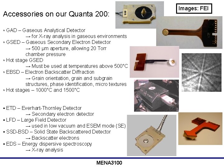
Accessories on our Quanta 200: ◦ GAD – Gaseous Analytical Detector → for X-ray analysis in gaseous environments ◦ GSED – Gaseous Secondary Electron Detector → 500 μm aperture, allowing 20 Torr chamber pressure ◦ Hot stage GSED → Must be used at temperatures above 500°C ◦ EBSD – Electron Backscatter Diffraction → Grain orientation, grain and subgrain structures, phase identification, micro textures ◦ Hot stages – 1000°C and 1500°C ▪ ETD – Everhart-Thornley Detector → Secondary electron detector ▪ LFD – Large Field Detector → used in low vacuum and ESEM mode (SE) ▪ SSD-BSD – Solid State Backscattered Detector → Backscatter electrons ▪ EDS – Energy dispersive spectroscopy → X-ray analysis MENA 3100 Images: FEI

Some comments on resolution • Best resolution that can be obtained: size of the electron spot on the sample surface – The introduction of FEG has dramatically improved the resolution of SEM’s • The volume from which the signal electrons are formed defines the resolution – SE image has higher resolution than a BSE image • Scanning speed: – a weak signal requires slow speed to improve signalto-noise ratio – when doing a slow scan drift in the electron beam can affect the accuracy of the analysis MENA 3100

What have we not covered in this presentation • Sample preparation • Details on the electromagnetic optics • Alternative imaging modes: – Cathodoluminescence – Electron beam induces current – Orientation imaging microscopy (available at Ui. O) • Focused ion beam microscopy MENA 3100

Summary • The scanning electron microscope is a versatile instrument that can be used for many purposes and can be equipped with various accessories • An electron probe is scanned across the surface of the sample and detectors interpret the signal as a function of time • A resolution of 1 – 2 nm can be obtained when operated in a high resolution setup • The introduction of ESEM and the field emission gun have simplified the imaging of challenging samples MENA 3100

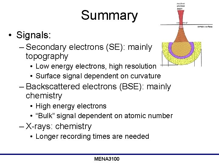
Summary • Signals: – Secondary electrons (SE): mainly topography • Low energy electrons, high resolution • Surface signal dependent on curvature – Backscattered electrons (BSE): mainly chemistry • High energy electrons • “Bulk” signal dependent on atomic number – X-rays: chemistry • Longer recording times are needed MENA 3100