San Sebastian November 27 2017 The route from
San Sebastian, November 27, 2017 The route from fundamental science to technological innovation (and the wonders of doing research) A few examples of routes from science to innovations in the Technologies of Information and Communication
First example: the route from fundamental research on electrical conduction in magnetic metals to the “big data” stored today on hard disks (and the birth of spin electronics) Second example: from quantum physics to low power computers and telephones
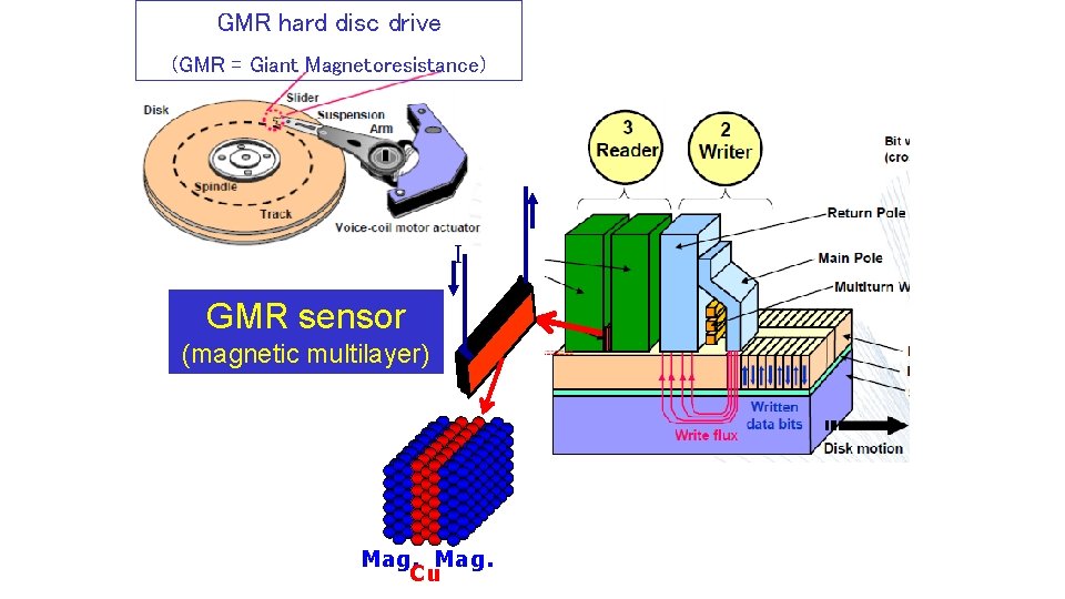
GMR hard disc drive (GMR = Giant Magnetoresistance) I GMR sensor (magnetic multilayer) Mag. Cu
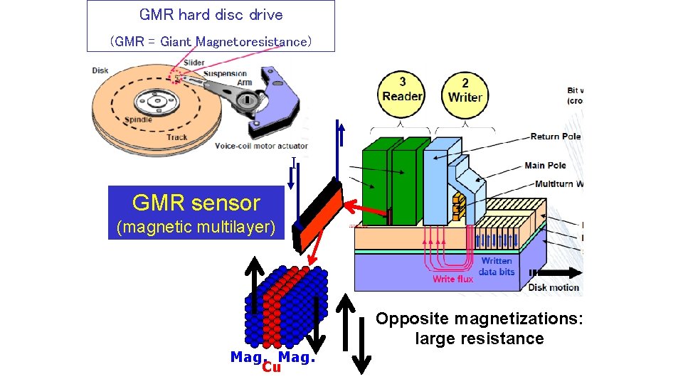
GMR hard disc drive (GMR = Giant Magnetoresistance) I GMR sensor (magnetic multilayer) Mag. Cu Opposite magnetizations: large resistance

GMR hard disc drive (GMR = Giant Magnetoresistance) I GMR sensor (magnetic multilayer) Mag. Cu Parallel magnetizations: small resistance
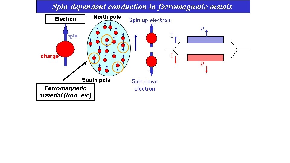
Spin dependent conduction in ferromagnetic metals North pole Electron Spin up electron I spin I charge South pole Ferromagnetic material (Iron, etc) Spin down electron
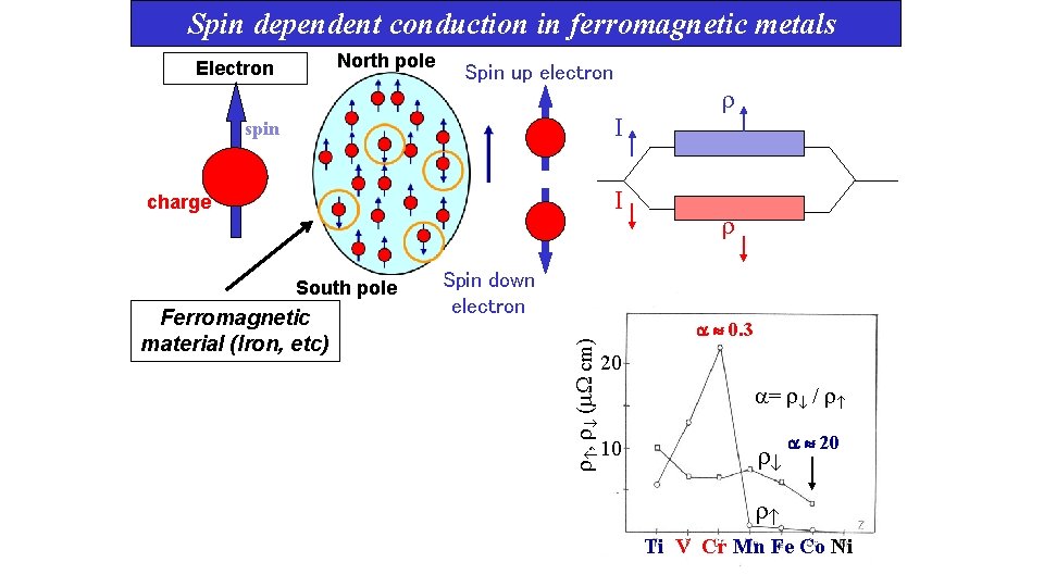
Spin dependent conduction in ferromagnetic metals North pole Electron Spin up electron I spin I charge Ferromagnetic material (Iron, etc) Spin down electron , ( cm) South pole 0. 3 20 = / 10 20 Ti V Cr Mn Fe Co Ni
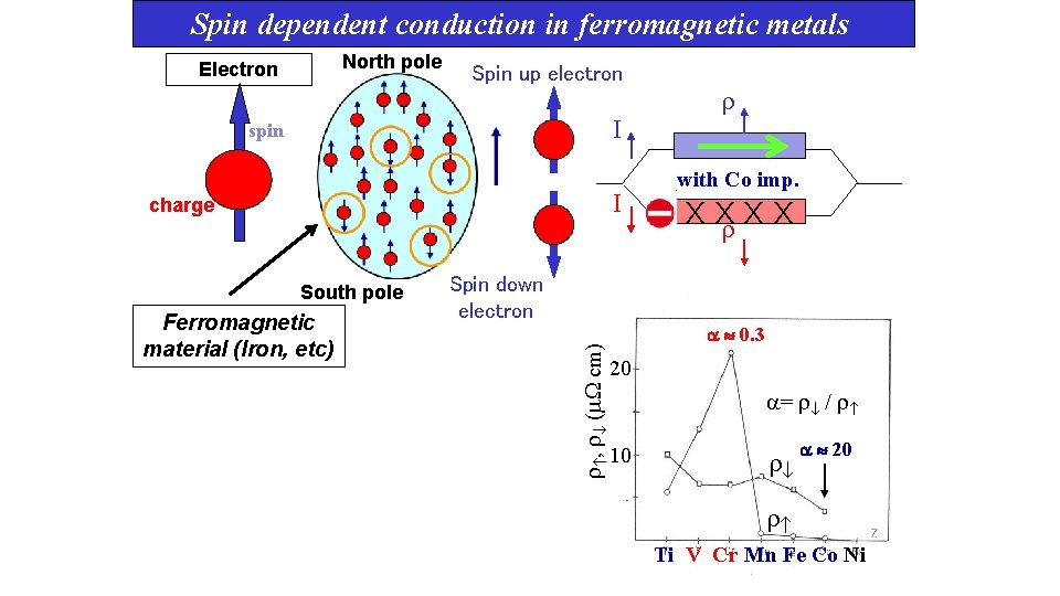
Spin dependent conduction in ferromagnetic metals North pole Electron Spin up electron I spin I charge Ferromagnetic material (Iron, etc) Spin down electron , ( cm) South pole with Co imp. X X 0. 3 20 = / 10 20 Ti V Cr Mn Fe Co Ni
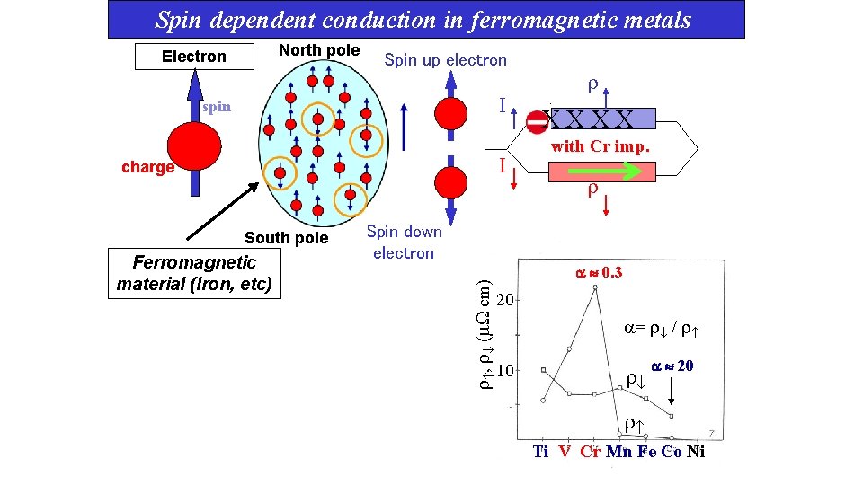
Spin dependent conduction in ferromagnetic metals North pole Electron Spin up electron I spin I charge Ferromagnetic material (Iron, etc) Spin down electron , ( cm) South pole X X with Cr imp. 0. 3 20 = / 10 20 Ti V Cr Mn Fe Co Ni
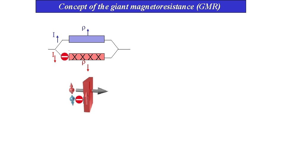
Concept of the giant magnetoresistance (GMR) I I X X
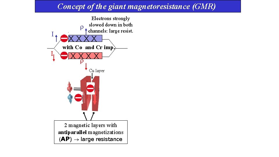
Concept of the giant magnetoresistance (GMR) I I Electrons strongly slowed down in both channels: large resist. X X with Co and Cr imp. X X Cu layer 2 magnetic layers with antiparallel magnetizations (AP) large resistance
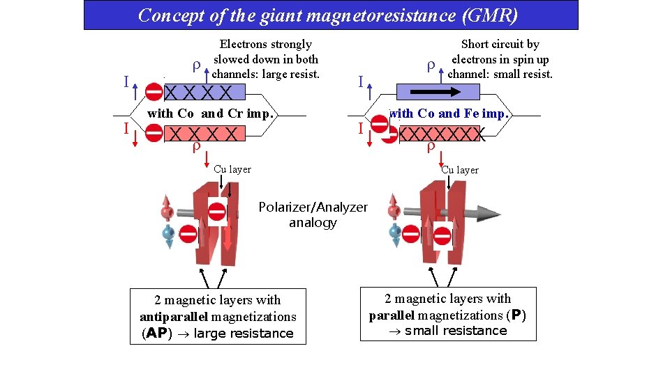
Concept of the giant magnetoresistance (GMR) I I Electrons strongly slowed down in both channels: large resist. X X with Co and Cr imp. X X I I Cu layer Short circuit by electrons in spin up channel: small resist. with Co and Fe imp. XXXXXXX Cu layer Polarizer/Analyzer analogy 2 magnetic layers with antiparallel magnetizations (AP) large resistance 2 magnetic layers with parallel magnetizations (P) small resistance
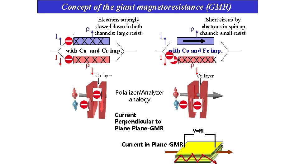
Concept of the giant magnetoresistance (GMR) I I Electrons strongly slowed down in both channels: large resist. X X with Co and Cr imp. X X I I Short circuit by electrons in spin up channel: small resist. with Co and Fe imp. XXXXXXX Cu layer Polarizer/Analyzer analogy Current Perpendicular to Plane-GMR Current in Plane-GMR V=RI
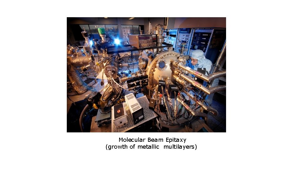
Molecular Beam Epitaxy (growth of metallic multilayers)
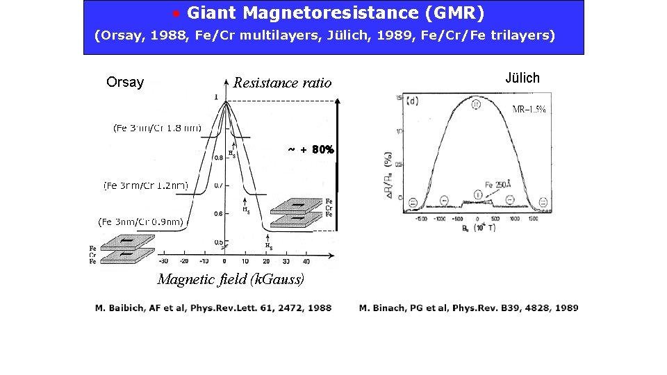
• Giant Magnetoresistance (GMR) (Orsay, 1988, Fe/Cr multilayers, Jülich, 1989, Fe/Cr/Fe trilayers) Orsay Resistance ratio ~ + 80% Magnetic field (k. Gauss) Jülich
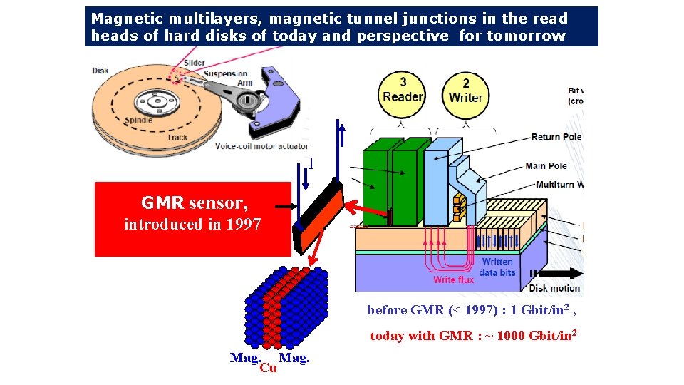
Magnetic multilayers, magnetic tunnel junctions in the read heads of hard disks of today and perspective for tomorrow I GMR sensor, introduced in 1997 before GMR (< 1997) : 1 Gbit/in 2 , today with GMR : ~ 1000 Gbit/in 2 Mag. Cu
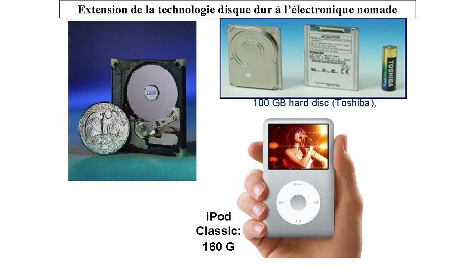
Extension de la technologie disque dur à l’électronique nomade 100 GB hard disc (Toshiba), i. Pod Classic: 160 G
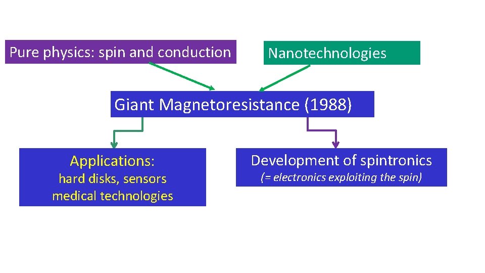
Pure physics: spin and conduction Nanotechnologies Giant Magnetoresistance (1988) Applications: hard disks, sensors medical technologies Development of spintronics (= electronics exploiting the spin)
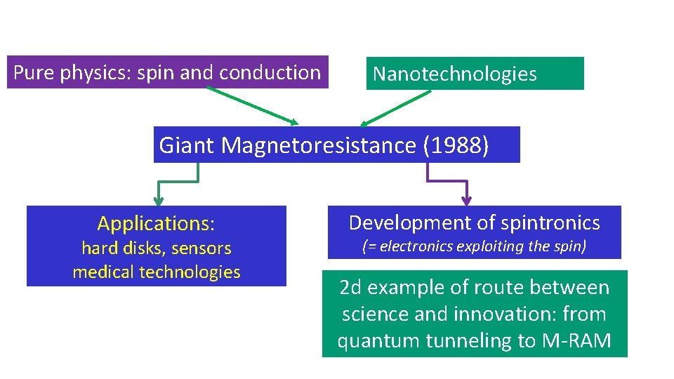
Pure physics: spin and conduction Nanotechnologies Giant Magnetoresistance (1988) Applications: hard disks, sensors medical technologies Development of spintronics (= electronics exploiting the spin) 2 d example of route between science and innovation: from quantum tunneling to M-RAM
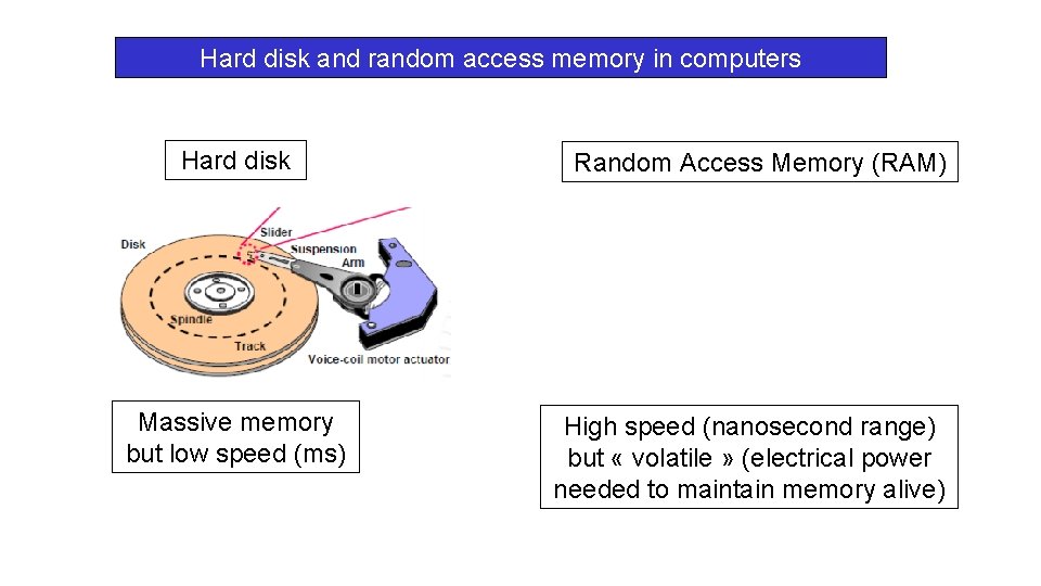
Hard disk and random access memory in computers Hard disk Massive memory but low speed (ms) Random Access Memory (RAM) High speed (nanosecond range) but « volatile » (electrical power needed to maintain memory alive)
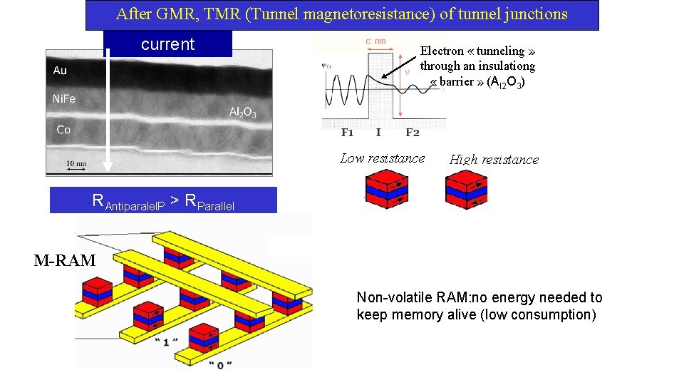
After GMR, TMR (Tunnel magnetoresistance) of tunnel junctions current Electron « tunneling » through an insulationg « barrier » (Al 2 O 3) Low resistance High resistance RAntiparalel. P > RParallel M-RAM Non-volatile RAM: no energy needed to keep memory alive (low consumption)
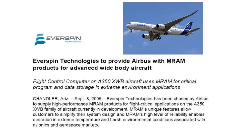
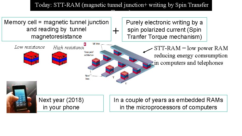
Today: STT-RAM (magnetic tunnel junction+ writing by Spin Transfer Torque) Memory cell = magnetic tunnel junction and reading by tunnel magnetoresistance Low resistance High resistance Next year (2018) in your phone + Purely electronic writing by a spin polarized current (Spin Tranfer Torque mechanism) STT-RAM = low power RAM reducing energy comsumption in computers and telephones In a couple of years as embedded RAMs in the microprocessors of computers
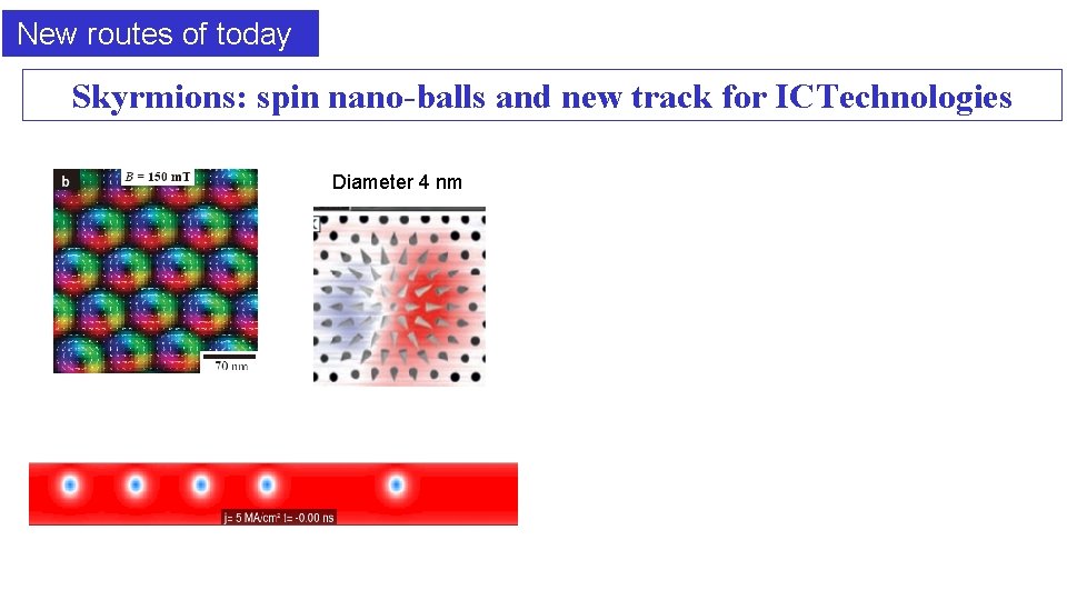
New routes of today Skyrmions: spin nano-balls and new track for ICTechnologies Diameter 4 nm
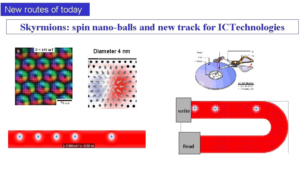
New routes of today Skyrmions: spin nano-balls and new track for ICTechnologies Diameter 4 nm write Read
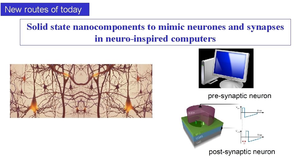
New routes of today Solid state nanocomponents to mimic neurones and synapses in neuro-inspired computers

I thank you for your attention
- Slides: 27