Rutherford Appleton Laboratory Particle Physics Department Design and
Rutherford Appleton Laboratory Particle Physics Department Design and Characterization of a Novel, Radiation. Resistant Active Pixel Sensor in a Standard 0. 25 m CMOS Technology P. P. Allport, G. Casse, A. Evans, M. Tyndel, R. Turchetta, J. J. Velthuis, G. Villani IEEE NSS Rome, October 2004
Rutherford Appleton Laboratory Particle Physics Department Outline • • CMOS APS detectors: principle & characteristics Novel CMOS detector structure HEPAPS 3 Conclusions G. Villani IEEE NSS Rome, October 2004
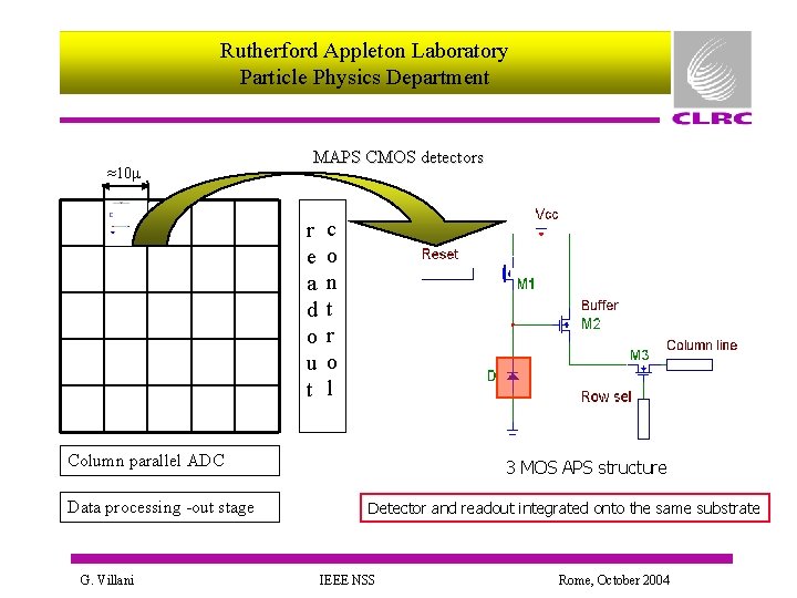
Rutherford Appleton Laboratory Particle Physics Department ≈10 MAPS CMOS detectors r e a d o u t c o n t r o l Column parallel ADC Data processing -out stage G. Villani 3 MOS APS structure Detector and readout integrated onto the same substrate IEEE NSS Rome, October 2004

Rutherford Appleton Laboratory Particle Physics Department CMOS detectors for HEP Nwell - + - Pepi - + - Pwell - + + + - P++ Generated charge diffuses through epitaxial layer and substrate until recombines or gets collected by cathode G. Villani Internal electric field 3 D view Vbias = 2 V applied to N+ Well 30 ns Transient Electron Current IEEE NSS Rome, October 2004
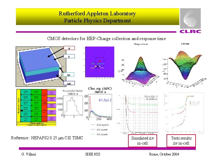
Rutherford Appleton Laboratory Particle Physics Department CMOS detectors for HEP-Charge collection and response time N P epi subs Reference : HEPAPS 2 0. 25 μm CIS TSMC G. Villani Simulated ∆v in-cell IEEE NSS Tests results ∆v in-cell Rome, October 2004

Rutherford Appleton Laboratory Particle Physics Department CMOS detectors for HEP-Radiation Hardness T = 300 K T = 253 K No RAD 1014 J. Velthuis University of Liverpool Example of simulation radiation degradation @ to bulk damage Ф = 1014 24 Ge. V p Example of S/N calculation under Hard Reset assumption V bias = 2 V HEPAPS 2 0. 25 μm CIS TSMC Test results S/N ratio vs number of pixels Charge collected mainly by diffusion: Radiation Bulk damage seriously impacts onto charge collection efficiency G. Villani IEEE NSS Rome, October 2004
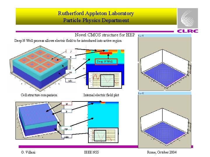
Rutherford Appleton Laboratory Particle Physics Department Novel CMOS structure for HEP Deep N Well process allows electric field to be introduced into active region Deep N Well Cell structure comparison Internal electric field plot N P epi subs G. Villani IEEE NSS Rome, October 2004
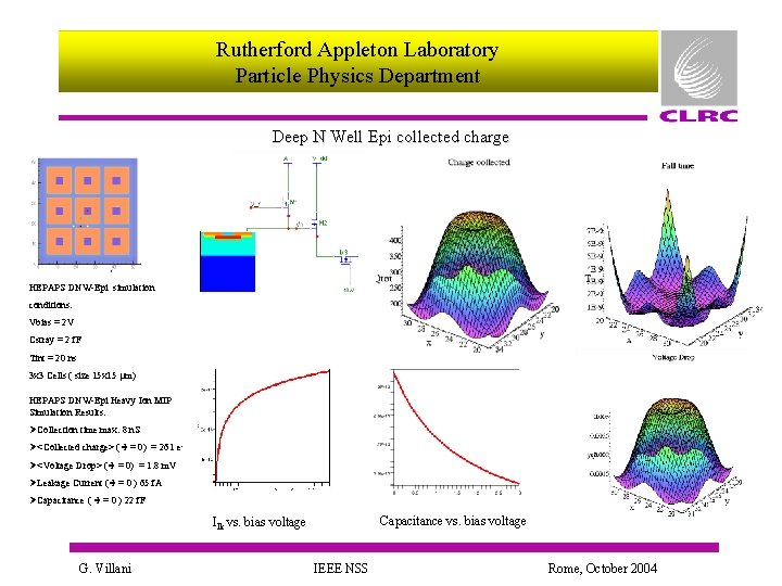
Rutherford Appleton Laboratory Particle Physics Department Deep N Well Epi collected charge HEPAPS DNW-Epi simulation conditions: Vbias = 2 V Cstray = 2 f. F Tint = 20 ns 3 x 3 Cells ( size 15 x 15 m) HEPAPS DNW-Epi Heavy Ion MIP Simulation Results: ØCollection time max: 8 n. S Ø<Collected charge> (Ф = 0) = 261 eØ<Voltage Drop> (Ф = 0) = 1. 8 m. V ØLeakage Current (Ф = 0 ) 65 f. A ØCapacitance ( Ф = 0 ) 22 f. F Capacitance vs. bias voltage Ilk vs. bias voltage G. Villani IEEE NSS Rome, October 2004
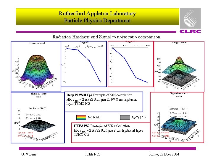
Rutherford Appleton Laboratory Particle Physics Department Radiation Hardness and Signal to noise ratio comparison Deep N Well Epi Example of S/N calculation HR Vbias = 2 APS 2 0. 25 μm DNW 8 m Epitaxial layer TSMC MS No RAD 1014 HEPAPS 2 Example of S/N calculation HR Vbias = 2 APS 2 0. 25 μm 8 m Epitaxial layer TSMC CIS G. Villani IEEE NSS Rome, October 2004
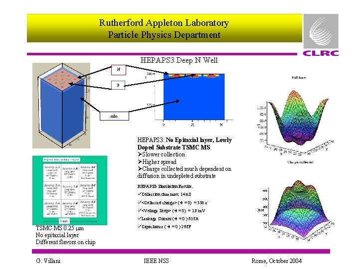
Rutherford Appleton Laboratory Particle Physics Department HEPAPS 3 Deep N Well N P subs HEPAPS 3: HEPAPS 3 No Epitaxial layer, Lowly Doped Substrate TSMC MS ØSlower collection ØHigher spread ØCharge collected much dependent on diffusion in undepleted substrate HEPAPS 3 Simulation Results: üCollection time max: 14 n. S ü<Collected charge> (Ф = 0) = 338 eü<Voltage Drop> (Ф = 0) = 1. 9 m. V üLeakage Current (Ф = 0 ) 65 f. A TSMC MS 0. 25 m No epitaxial layer Different flavors on chip G. Villani üCapacitance ( Ф = 0 ) 26 f. F IEEE NSS Rome, October 2004
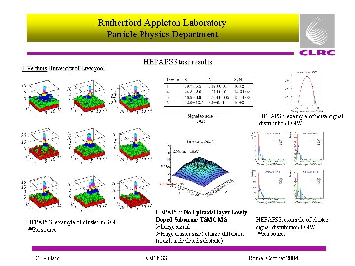
Rutherford Appleton Laboratory Particle Physics Department J. Velthuis University of Liverpool HEPAPS 3 test results HEPAPS 3: example of noise signal distribution DNW HEPAPS 3: example of cluster in S/N 106 Ru source G. Villani HEPAPS 3: No Epitaxial layer Lowly Doped Substrate TSMC MS ØLarge signal ØHuge cluster size( charge diffusion trough undepleted substrate) IEEE NSS HEPAPS 3: example of cluster signal distribution DNW 106 Ru source Rome, October 2004
Rutherford Appleton Laboratory Particle Physics Department Conclusions üTopology optimization of MAPS still ongoing, but future HEP experiments call for uncompromisingly high radiation resistant structures üDeep N Well with Epitaxial layer introduces drift component in collection charge process üHEPAPS 3 preliminary tests results and simulations suggest Deep N Well process with epitaxial layer might show good performances at high level of radiation üSynergy between new design topologies and Deep N Well process required to fully exploit the potential benefits G. Villani IEEE NSS Rome, October 2004
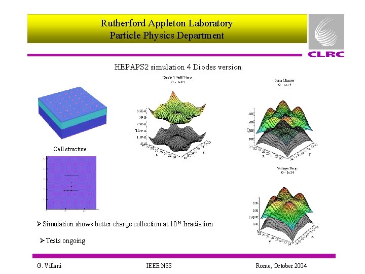
Rutherford Appleton Laboratory Particle Physics Department HEPAPS 2 simulation 4 Diodes version Cell structure ØSimulation shows better charge collection at 1014 Irradiation ØTests ongoing G. Villani IEEE NSS Rome, October 2004
- Slides: 13