
Rutherford Appleton Laboratory Particle Physics Department A MAPSbased
Rutherford Appleton Laboratory Particle Physics Department A MAPS-based readout for Tera. Pixel electromagnetic calorimeter at the ILC Y. Mikami, O. Miller, V. Rajovic, N. K. Watson, J. A. Wilson University of Birmingham J. A. Ballin, P. D. Dauncey, A. -M. Magnan, M. Noy Imperial College London J. P. Crooks, M. Stanitzki, K. D. Stefanov, R. Turchetta, M. Tyndel, E. G. Villani Rutherford Appleton Laboratory TWEPP-07 Topical Workshop on Electronics for Particle Physics Prague 2007 1 G. Villani CALICE MAPS Prague September 2007

Rutherford Appleton Laboratory Particle Physics Department Outline • ILC CALICE • CALICE MAPS Concept, R&D activity • Conclusions 2 G. Villani CALICE MAPS Prague September 2007
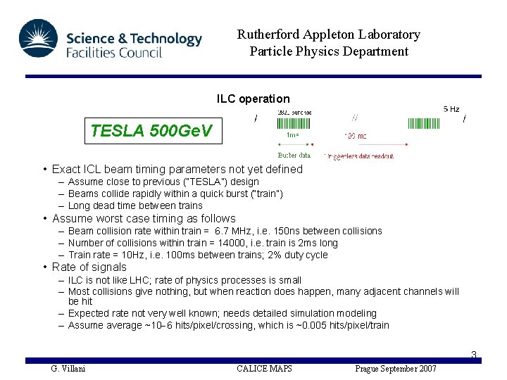
Rutherford Appleton Laboratory Particle Physics Department ILC operation TESLA 500 Ge. V • Exact ICL beam timing parameters not yet defined – Assume close to previous (“TESLA”) design – Beams collide rapidly within a quick burst (“train”) – Long dead time between trains • Assume worst case timing as follows – Beam collision rate within train = 6. 7 MHz, i. e. 150 ns between collisions – Number of collisions within train = 14000, i. e. train is 2 ms long – Train rate = 10 Hz, i. e. 100 ms between trains; 2% duty cycle • Rate of signals – ILC is not like LHC; rate of physics processes is small – Most collisions give nothing, but when reaction does happen, many adjacent channels will be hit – Expected rate not very well known; needs detailed simulation modeling – Assume average ~10 6 hits/pixel/crossing, which is ~0. 005 hits/pixel/train 3 G. Villani CALICE MAPS Prague September 2007

Rutherford Appleton Laboratory Particle Physics Department CALICE description • CALICE has a baseline ECAL design • Sampling calorimeter, alternating thick conversion layers (tungsten) and thin measurement layers (silicon) • Around 2 m radius, 4 m long, 30 layers tungsten and silicon, ≈2000 m 2 Si • Mechanical structure • Half of tungsten sheets embedded in carbon fibre structure • Other half of tungsten sandwiched between two PCBs each holding one layer of silicon detector wafers • Whole sandwich inserted into slots in carbon fibre structure 4 G. Villani CALICE MAPS Prague September 2007
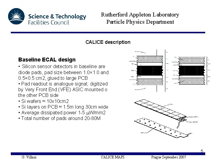
Rutherford Appleton Laboratory Particle Physics Department CALICE description Baseline ECAL design • Silicon sensor detectors in baseline are diode pads, pad size between 1. 0× 1. 0 and 0. 5× 0. 5 cm 2, glued to large PCB • Pad readout is analogue signal; digitized by Very Front End (VFE) ASIC mounted o the other PCB side • Si wafers ≈ 10 x 10 cm 2 • Si layers on PCB ≈ 1. 5 m long 30 cm wide • Average dissipated power 1 -5 W/mm 2 • Total number of pads around 20 -80 M 5 G. Villani CALICE MAPS Prague September 2007
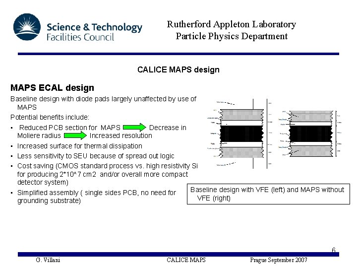
Rutherford Appleton Laboratory Particle Physics Department CALICE MAPS design MAPS ECAL design Baseline design with diode pads largely unaffected by use of MAPS Potential benefits include: • Reduced PCB section for MAPS Decrease in Moliere radius Increased resolution • Increased surface for thermal dissipation • Less sensitivity to SEU because of spread out logic • Cost saving (CMOS standard process vs. high resistivity Si for producing 2*10^7 cm 2 and/or overall more compact detector system) Baseline design with VFE (left) and MAPS without • Simplified assembly ( single sides PCB, no need for VFE (right) grounding substrate) 6 G. Villani CALICE MAPS Prague September 2007
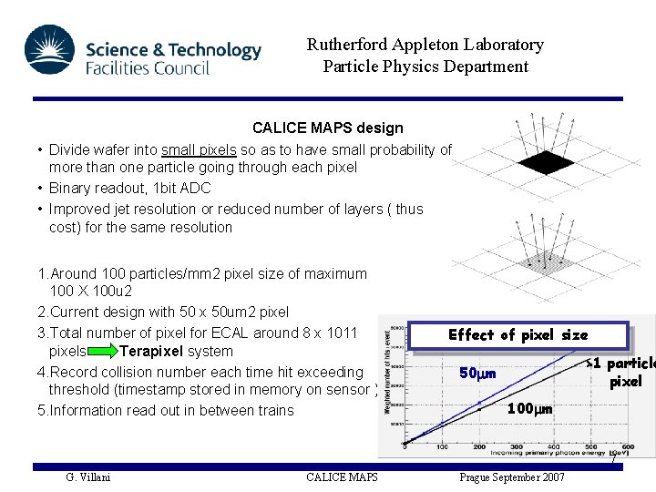
Rutherford Appleton Laboratory Particle Physics Department CALICE MAPS design • Divide wafer into small pixels so as to have small probability of more than one particle going through each pixel • Binary readout, 1 bit ADC • Improved jet resolution or reduced number of layers ( thus cost) for the same resolution 1. Around 100 particles/mm 2 pixel size of maximum 100 X 100 u 2 2. Current design with 50 x 50 um 2 pixel 3. Total number of pixel for ECAL around 8 x 1011 pixels Terapixel system 4. Record collision number each time hit exceeding threshold (timestamp stored in memory on sensor ) 5. Information read out in between trains Effect of pixel size >1 particle pixel 50 mm 100 mm 7 G. Villani CALICE MAPS Prague September 2007
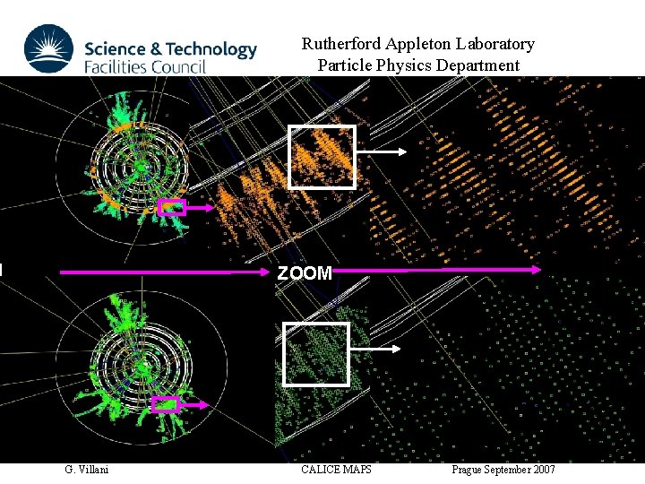
Rutherford Appleton Laboratory Particle Physics Department CALICE MAPS design 50 50 μm 2 MAPS pixels ZOOM Si. D 16 mm 2 area cells 8 G. Villani CALICE MAPS Prague September 2007
Rutherford Appleton Laboratory Particle Physics Department CALICE MAPS design • First prototype designed in CIS 0. 18 m process submitted early 2007 • Different pixel architectures included in the first prototype • Target is to reduce noise to the level of physics background (S/N>15) • Faulty pixels masking and variable threshold to reduce false hits and crosstalk • Optimization of pixel layout and topology essential • Minimization of power consumption essential 9 G. Villani CALICE MAPS Prague September 2007
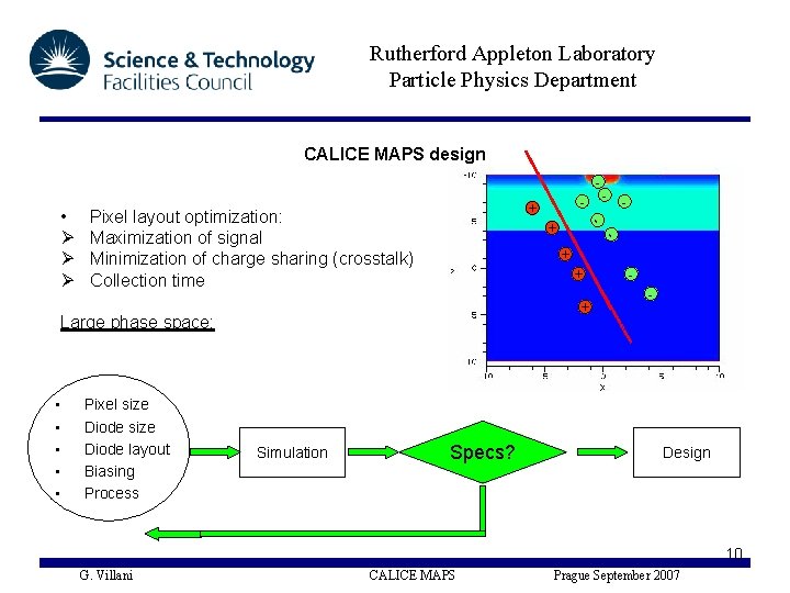
Rutherford Appleton Laboratory Particle Physics Department CALICE MAPS design - Pixel layout optimization: Maximization of signal Minimization of charge sharing (crosstalk) Collection time + - Pixel size Diode layout Biasing Process + + Simulation - + Large phase space: • • • - - • Ø Ø Ø - + Specs? - Design 10 G. Villani CALICE MAPS Prague September 2007
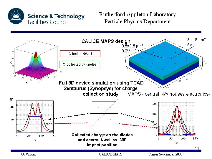
Rutherford Appleton Laboratory Particle Physics Department 1. 8 x 1. 8 m 2 1. 5 V CALICE MAPS design Q lost in NWell 3. 5 x 3. 5 m 2 3. 3 V Q collected by diodes Full 3 D device simulation using TCAD Sentaurus (Synopsys) for charge collection study MAPS - central NW houses electronics- e- Collected charge on the diodes and central Nwell vs. MIP impact position G. Villani CALICE MAPS 11 Prague September 2007
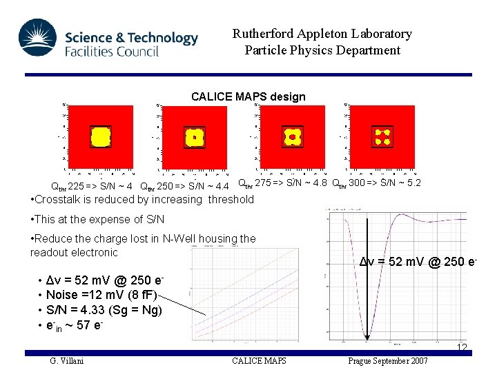
Rutherford Appleton Laboratory Particle Physics Department CALICE MAPS design Qthr 225 => S/N ~ 4 Qthr 250 => S/N ~ 4. 4 Qthr 275 => S/N ~ 4. 8 Qthr 300 => S/N ~ 5. 2 • Crosstalk is reduced by increasing threshold • This at the expense of S/N • Reduce the charge lost in N-Well housing the readout electronic Δv = 52 m. V @ 250 e- • Δv = 52 m. V @ 250 e • Noise =12 m. V (8 f. F) • S/N = 4. 33 (Sg = Ng) • e-in ~ 57 e 12 G. Villani CALICE MAPS Prague September 2007
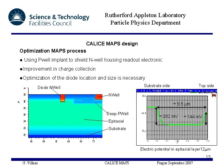
Rutherford Appleton Laboratory Particle Physics Department CALICE MAPS design Optimization MAPS process ● Using Pwell implant to shield N-well housing readout electronic ●Improvement in charge collection ●Optimization of the diode location and size is necessary Substrate side Diode NWell Top side NWell ≈ 9. 5 μm Deep-PWell Epitaxial ≈ 202 m. V ≈ 144 m. V Substrate Electric potential in epitaxial layer 12 m 13 G. Villani CALICE MAPS Prague September 2007
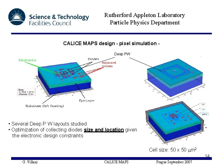
Rutherford Appleton Laboratory Particle Physics Department CALICE MAPS design - pixel simulation Deep PW 1. 8 x 1. 8 m 2 0 V • Several Deep P W layouts studied • Optimization of collecting diodes size and location given the electronic design constraints Cell size: 50 x 50 m 2 14 G. Villani CALICE MAPS Prague September 2007
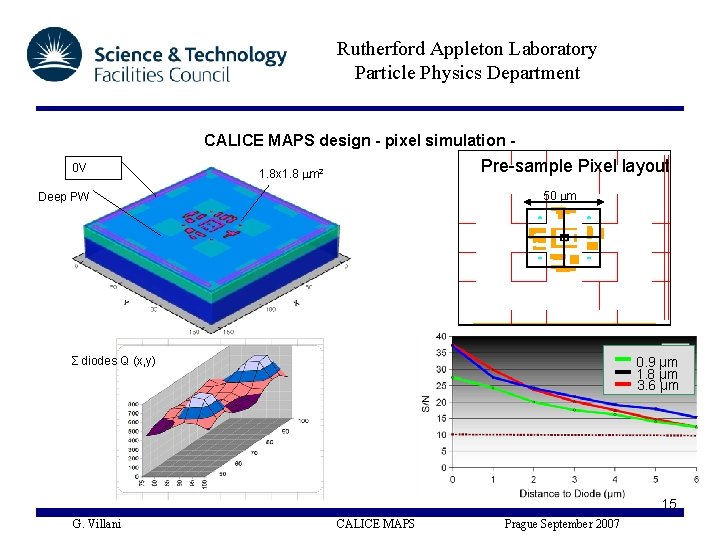
Rutherford Appleton Laboratory Particle Physics Department CALICE MAPS design - pixel simulation 0 V Pre-sample Pixel layout 1. 8 x 1. 8 m 2 50 m Deep PW Σ diodes Q (x, y) 0. 9 μm 1. 8 μm 3. 6 μm 15 G. Villani CALICE MAPS Prague September 2007
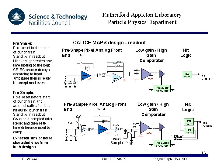
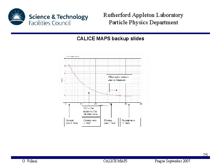
Rutherford Appleton Laboratory Particle Physics Department Pre-Shape: Pixel reset before start of bunch train Stand by in readout Hit event generates one time hit-flag to the logic CR-RC shaper decays according to input amplitude then is ready to accept next event Pre-Sample: Pixel reset before start of bunch train and automatically after local hit during bunch train Stand by in readout CA output sampled after Reset and then realtime difference input to comp Expected similar noise characteristics from both designs CALICE MAPS design - readout Pre-Shape Pixel Analog Front Rst End Low gain / High Gain Comparator Rfb Cpr e Vth+ Vth- Cin Rin Pream p Hit Logic 150 ns Shap er Hit Output Trim&Mask SRAM SR Pre-Sample Pixel Analog Front Pre. Rst End Low gain / High Gain Comparator Vrst Rst Cfb Buffe r s. f Cin Shaper 150 ns Vth+ Vth- Buffe r s. f Reset Sample Hit Logic Self Reset Cstore Hit Output 450 ns Trim&Mask SRAM SR 16 G. Villani CALICE MAPS Prague September 2007
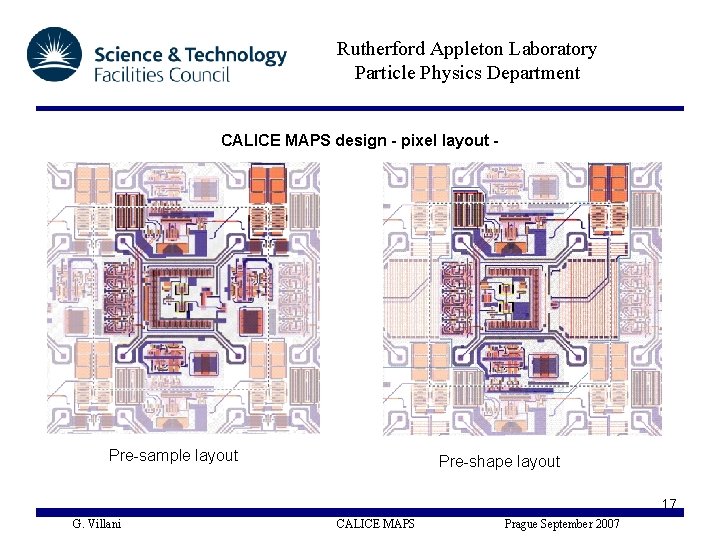
Rutherford Appleton Laboratory Particle Physics Department CALICE MAPS design - pixel layout - Pics of layouts Pre-sample layout Pre-shape layout 17 G. Villani CALICE MAPS Prague September 2007
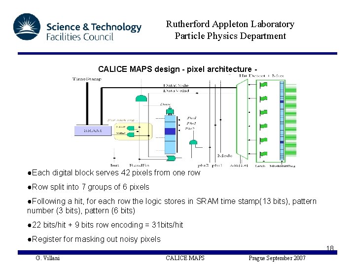
Rutherford Appleton Laboratory Particle Physics Department CALICE MAPS design - pixel architecture - ●Each digital block serves 42 pixels from one row ●Row split into 7 groups of 6 pixels ●Following a hit, for each row the logic stores in SRAM time stamp(13 bits), pattern number (3 bits), pattern (6 bits) ● 22 bits/hit + 9 bits row encoding = 31 bits/hit ●Register for masking out noisy pixels 18 G. Villani CALICE MAPS Prague September 2007
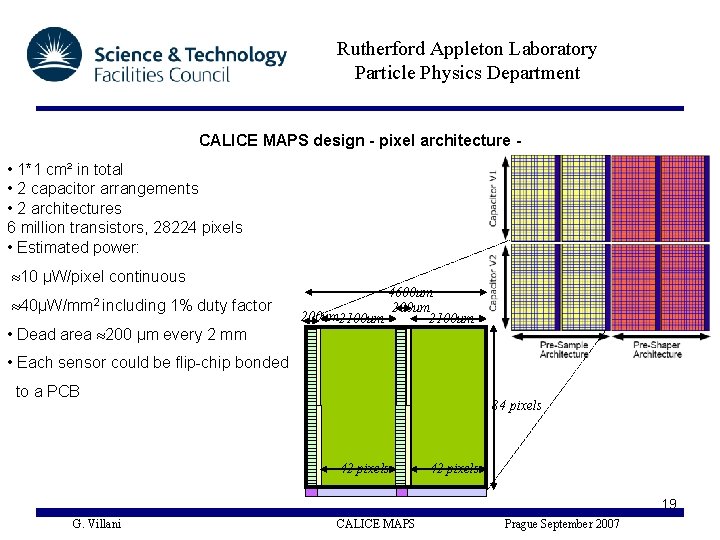
Rutherford Appleton Laboratory Particle Physics Department CALICE MAPS design - pixel architecture - • 1*1 cm² in total • 2 capacitor arrangements • 2 architectures 6 million transistors, 28224 pixels • Estimated power: 10 μW/pixel continuous 40μW/mm 2 including 1% duty factor • Dead area 200 μm every 2 mm 4600 um 200 um 2100 um • Each sensor could be flip-chip bonded to a PCB 84 pixels 42 pixels 19 G. Villani CALICE MAPS Prague September 2007
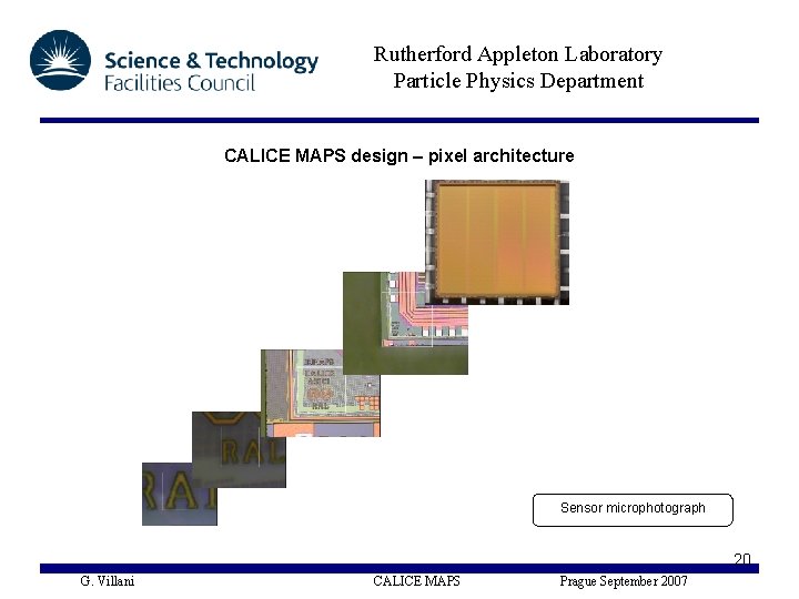
Rutherford Appleton Laboratory Particle Physics Department CALICE MAPS design – pixel architecture Sensor microphotograph 20 G. Villani CALICE MAPS Prague September 2007
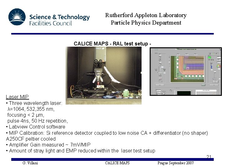
Rutherford Appleton Laboratory Particle Physics Department CALICE MAPS - RAL test setup - Laser MIP • Three wavelength laser: λ=1064, 532, 355 nm, focusing < 2 μm, pulse 4 ns, 50 Hz repetition, • Labview Control software • MIP Calibration: Si reference detector coupled to low noise CA + differentiator (no shaper) A 250 CF peltier cooled • Amplifier Gain measured ~ 7 m. V/MIP • Amount of stray light and EMP reduced within the laser test setup 21 G. Villani CALICE MAPS Prague September 2007
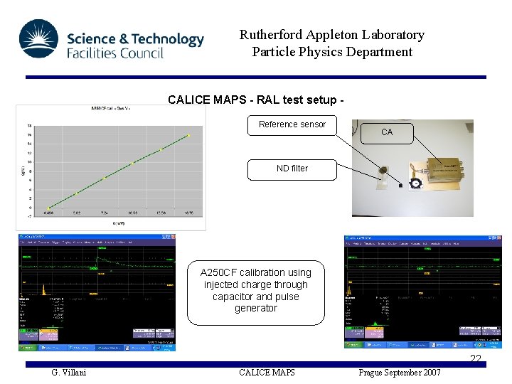
Rutherford Appleton Laboratory Particle Physics Department CALICE MAPS - RAL test setup Reference sensor CA ND filter A 250 CF calibration using injected charge through capacitor and pulse generator 22 G. Villani CALICE MAPS Prague September 2007
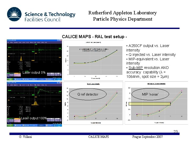
Rutherford Appleton Laboratory Particle Physics Department CALICE MAPS - RAL test setup • A 250 CF output vs. Laser intensity • Q injected vs. Laser intensity • MIP-equivalent vs. Laser intensity • Sub-MIP resolution AND accuracy capability (λ = 1064 nm, spot size = 2μm) Laser output 0% Q ref detector MIP ‘noise’ Laser output 100% 23 G. Villani CALICE MAPS Prague September 2007
Rutherford Appleton Laboratory Particle Physics Department Conclusions • • MAPS-based ECAL can potentially offer a number of advantages in terms of performances and overall cost Novel INMAPS process for MAPS might have significant advantages in terms of charge collection efficiency Pixel design and readout electronics optimized for charge collection and S/N First design aims at demonstrating feasibility of the approach and to achieve significantly high S/N Power dissipation still high and needs to be addressed Test setup ready Chip testing underway now 24 G. Villani CALICE MAPS Prague September 2007
Rutherford Appleton Laboratory Particle Physics Department CALICE MAPS backup slides 25 G. Villani CALICE MAPS Prague September 2007
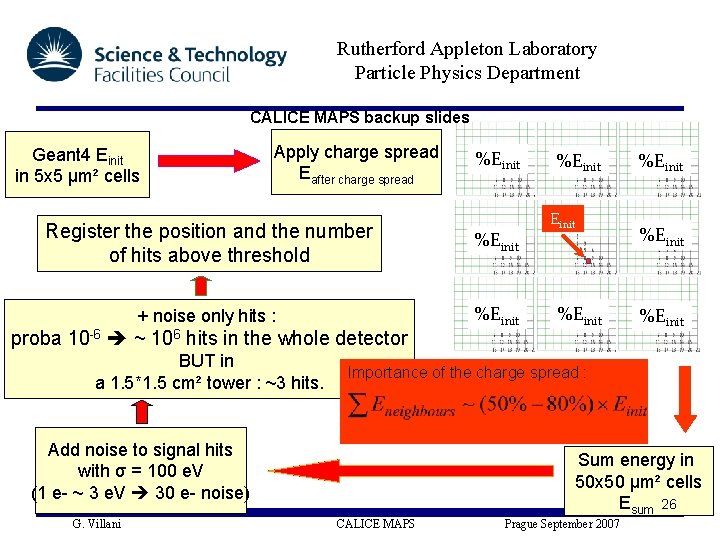
Rutherford Appleton Laboratory Particle Physics Department CALICE MAPS backup slides Geant 4 Einit in 5 x 5 μm² cells Apply charge spread Eafter charge spread %Einit Register the position and the number of hits above threshold %Einit + noise only hits : %Einit proba 10 -6 ~ 106 hits in the whole detector BUT in a 1. 5*1. 5 cm² tower : ~3 hits. Einit %Einit Importance of the charge spread : Add noise to signal hits with σ = 100 e. V (1 e- ~ 3 e. V 30 e- noise) G. Villani %Einit Sum energy in 50 x 50 μm² cells Esum 26 CALICE MAPS Prague September 2007
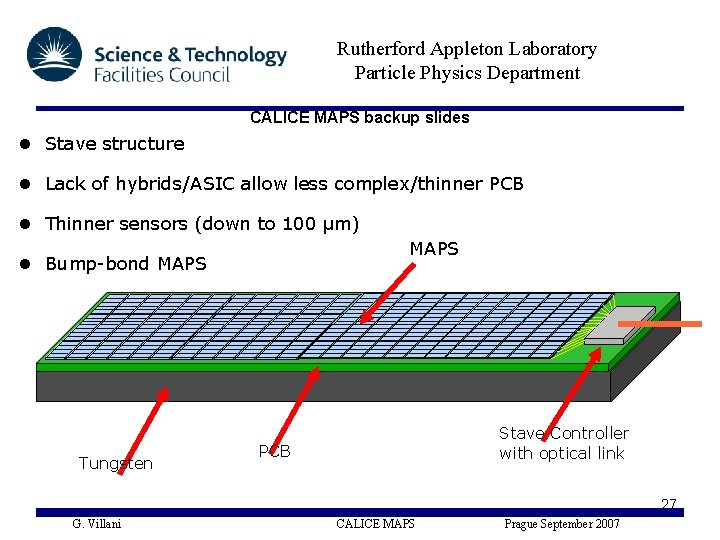
Rutherford Appleton Laboratory Particle Physics Department CALICE MAPS backup slides Stave structure Lack of hybrids/ASIC allow less complex/thinner PCB Thinner sensors (down to 100 µm) MAPS Bump-bond MAPS Tungsten Stave Controller with optical link PCB 27 G. Villani CALICE MAPS Prague September 2007
- Slides: 27