
RLS essentials Leonid Kraginskiy Strategic CAD Labs Intel
RLS essentials Leonid Kraginskiy Strategic CAD Labs Intel Corporation
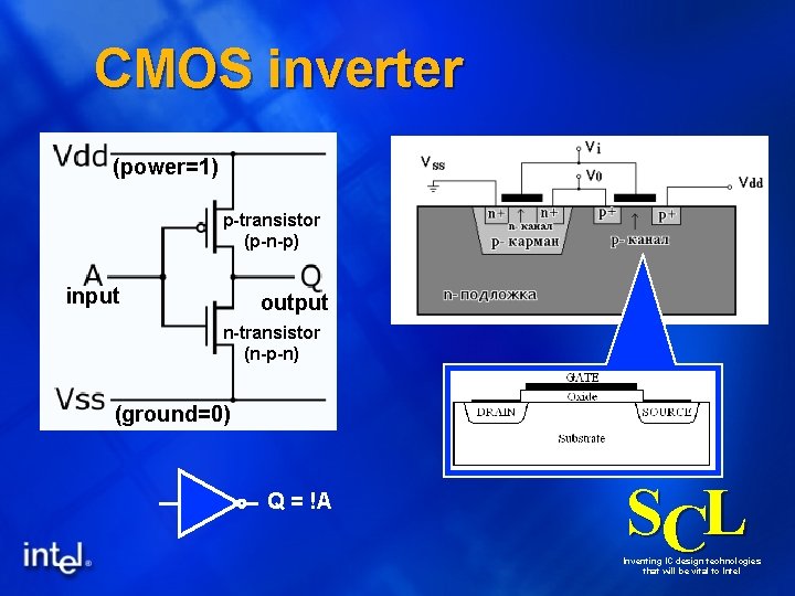
CMOS inverter (power=1) p-transistor (p-n-p) input output n-transistor (n-p-n) (ground=0) Q = !A SCL Inventing IC design technologies that will be vital to Intel
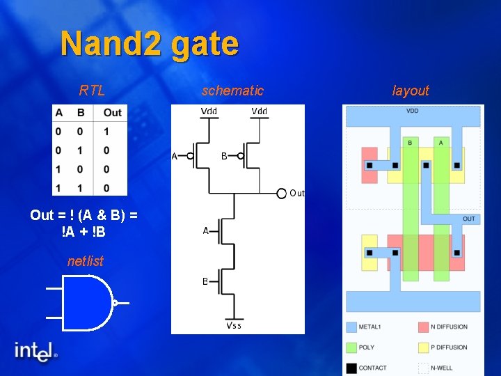
Nand 2 gate RTL schematic layout Out = ! (A & B) = !A + !B netlist SCL Inventing IC design technologies that will be vital to Intel
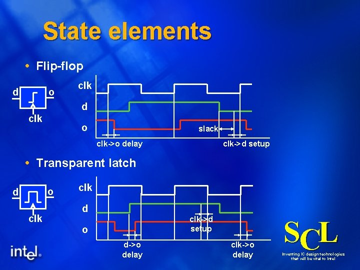
State elements Flip-flop d o clk d clk o slack clk->o delay clk->d setup Transparent latch o d clk->d setup o d->o delay clk->o delay SCL Inventing IC design technologies that will be vital to Intel
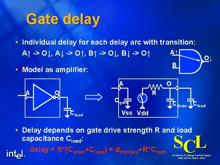
Gate delay Individual delay for each delay arc with transition: A↑ A↑ -> O↓, A↓ -> O↑, B↑ -> O↓, B↓ -> O↑ B Model as amplifier: A A O↓ O O R Cgate Cload Cdrain Cload Vss Vdd Delay depends on gate drive strength R and load capacitance Cload: delay = R*(Cdrain+Cload) = dintrinsic+R*Cload SCL Inventing IC design technologies that will be vital to Intel

Gate delay (2) Input pin (gate) capacitance is a given number for each pin Take into account signal slopes: V 1 V 2 Vdd output signal and its interpolation input signal t 0 t t 1+t 2 t Elaborated delay model (for each delay arc): SCL Inventing IC design technologies that will be vital to Intel
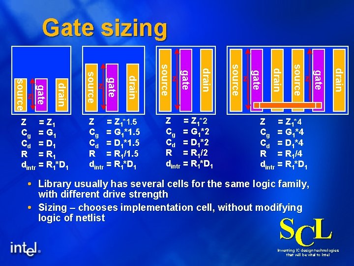
Gate sizing drain z gate source drain z gate Z = Z 1*2 Cg = G 1*2 Cd = D 1*2 R = R 1/2 dintr = R 1*D 1 source drain z gate Z = Z 1*1. 5 Cg = G 1*1. 5 Cd = D 1*1. 5 R = R 1/1. 5 dintr = R 1*D 1 source drain gate Z = Z 1 Cg = G 1 Cd = D 1 R = R 1 dintr = R 1*D 1 source drain gate source z z Z = Z 1*4 Cg = G 1*4 Cd = D 1*4 R = R 1/4 dintr = R 1*D 1 Library usually has several cells for the same logic family, with different drive strength Sizing – chooses implementation cell, without modifying logic of netlist SCL Inventing IC design technologies that will be vital to Intel
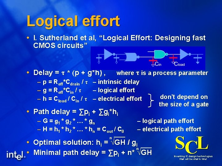
Logical effort I. Sutherland et al, “Logical Effort: Designing fast CMOS circuits” Delay = τ * (p + g*h) , where τ is a process parameter – p = Reff*Cdrain / τ – intrinsic delay – g = Reff*Cin / τ – logical effort don’t depend on – h = Cload / Cin / τ – electrical effort the size of a gate Path delay = ∑pi + ∑gi*hi – G = g 1 * g 2 * … * gn – H = h 1 * h 2 * … * hn = Cout / C 0 n – logical path effort – electrical path effort Optimal solution: hi = √GH / gi n Minimal path delay = ∑pi + n* √GH SCL Inventing IC design technologies that will be vital to Intel
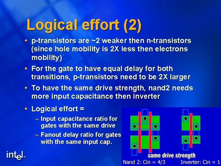
Logical effort (2) p-transistors are ~2 weaker then n-transistors (since hole mobility is 2 X less then electrons mobility) For the gate to have equal delay for both transitions, p-transistors need to be 2 X larger To have the same drive strength, nand 2 needs more input capacitance then inverter Logical effort = – Input capacitance ratio for gates with the same drive – Fanout delay ratio for gates with the same input cap. SCL Inventing IC design technologies that will be vital to Intel
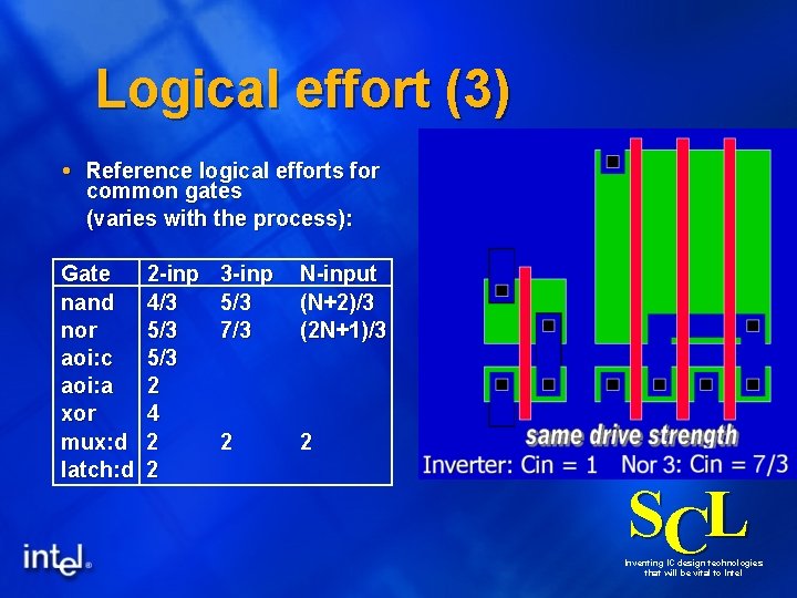
Logical effort (3) Reference logical efforts for common gates (varies with the process): Gate nand nor aoi: c aoi: a xor mux: d latch: d 2 -inp 4/3 5/3 2 4 2 2 3 -inp 5/3 7/3 N-input (N+2)/3 (2 N+1)/3 2 2 SCL Inventing IC design technologies that will be vital to Intel
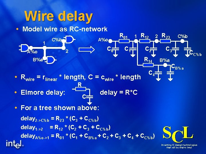
Wire delay Model wire as RC-network 1 C%b A%o C 0 2 R 01 1 R 12 C 1 C 2 R 14 B%a Rwire = rlinear * length, C = cwire * length C 4 2 R 23 C%b C 3 CC%b B%a CB%a R Elmore delay: C delay = R*C For a tree shown above: delay 2 ->C%b = R 23 * (C 3 + CC%b) delay 1 ->2 = R 12 * (C 2 + C 3 + CC%b) delay. A%o->1 = R 01 * (C 1 + CB%a + C 2 + C 3 + C 4 + CC%b) SCL Inventing IC design technologies that will be vital to Intel
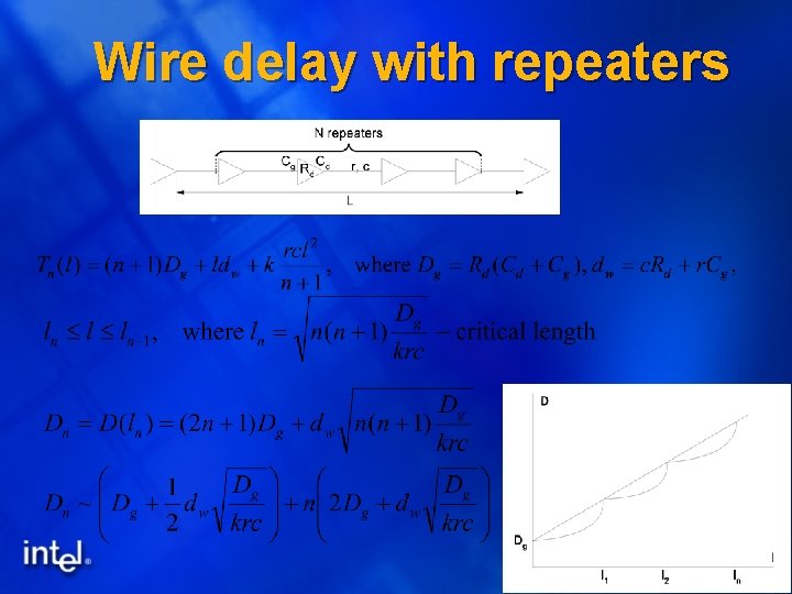
Wire delay with repeaters SCL Inventing IC design technologies that will be vital to Intel
Buffering Addresses 2 problems: – large (capacitive) fanout – long wires Electrical effort based – fast – does not consider wires Van Ginneken Algorithm – – – very slow for large fanout considers wires requires clustering for large fanout requires tree topology for each net solves each net independently (drawback) SCL Inventing IC design technologies that will be vital to Intel
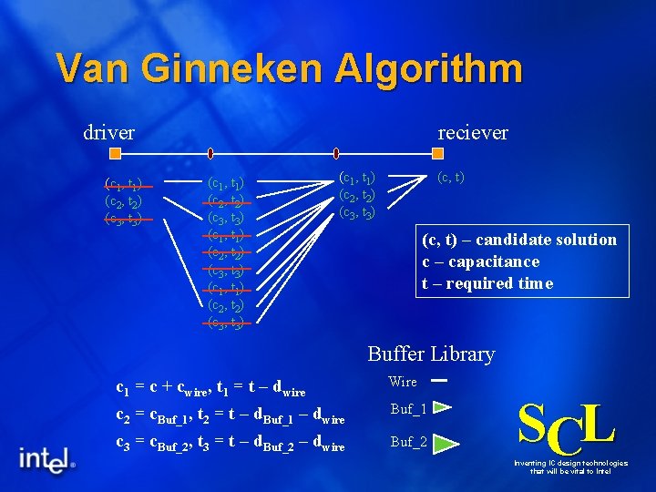
Van Ginneken Algorithm driver (c 1, t 1) (c 2, t 2) (c 3, t 3) reciever (c 1, t 1) (c 2, t 2) (c 3, t 3) (c, t) – candidate solution с – capacitance t – required time Buffer Library c 1 = c + cwire, t 1 = t – dwire c 2 = c. Buf_1, t 2 = t – d. Buf_1 – dwire c 3 = c. Buf_2, t 3 = t – d. Buf_2 – dwire Wire Buf_1 Buf_2 SCL Inventing IC design technologies that will be vital to Intel
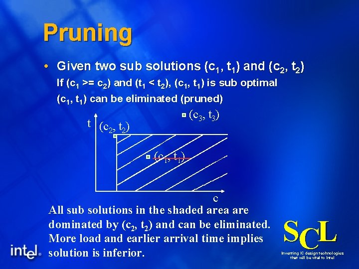
Pruning Given two sub solutions (c 1, t 1) and (c 2, t 2) If (c 1 >= c 2) and (t 1 < t 2), (c 1, t 1) is sub optimal (c 1, t 1) can be eliminated (pruned) (c 3, t 3) t (c 2, t 2) (c 1, t 1) c All sub solutions in the shaded area are dominated by (c 2, t 2) and can be eliminated. More load and earlier arrival time implies solution is inferior. SCL Inventing IC design technologies that will be vital to Intel

Dynamic Programming Algorithm – – – Start with base candidate solutions at receivers Propagate sub solutions up the routing tree Merge solutions from different branches Prune sub optimal solutions at intermediate nodes Pick optimal solution at driver and report the repeater solution in a downward traversal Merging: (c 1+c 3, min(t 1, t 3)) (c 1+c 4, min(t 1, t 4)) (c 2+c 3, min(t 2, t 3)) (c 2+c 4, min(t 2, t 4)) (c 1, t 1) (c 2, t 2) (c 3, t 3) (c 4, t 4) Dynamic programming – propagate only possibly optimal candidates SCL Inventing IC design technologies that will be vital to Intel
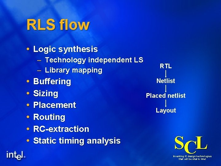
RLS flow Logic synthesis – Technology independent LS – Library mapping Buffering Sizing Placement Routing RC-extraction Static timing analysis RTL Netlist Placed netlist Layout SCL Inventing IC design technologies that will be vital to Intel
Placement Algorithm classes – Min-cut – Simulated annealing – Force-directed – Analytical – Genetic Net models – Star – Clique – Bush – Steiner tree SCL Inventing IC design technologies that will be vital to Intel
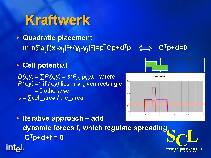
Kraftwerk Quadratic placement min∑aij[(xi-xj)²+(yi-yj)²]=p. TCp+d. Tp CTp+d=0 Cell potential D(x, y) = ∑Pi(x, y) – s*Pdie(x, y), where P(x, y) =1 if (x, y) lies in a given rectangle = 0 otherwise s = ∑cell_area / die_area Iterative approach – add dynamic forces f, which regulate spreading CTp+d+f = 0 SCL Inventing IC design technologies that will be vital to Intel
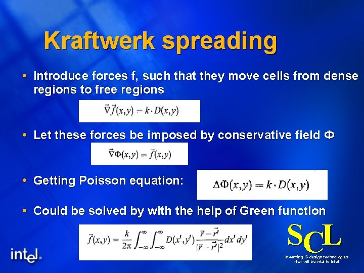
Kraftwerk spreading Introduce forces f, such that they move cells from dense regions to free regions Let these forces be imposed by conservative field Ф Getting Poisson equation: Could be solved by with the help of Green function SCL Inventing IC design technologies that will be vital to Intel
Analytical placement Solve constrained / unconstrained nonlinear optimization problem. Use smooth cost-function (approximation of TWL). Use grid structure to control spreading. Every bin g has a capacity cap(g) for cell area. Refine grid size with spreading. SCL Inventing IC design technologies that will be vital to Intel
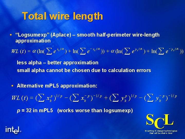
Total wire length “Logsumexp” (Aplace) – smooth half-perimeter wire-length approximation WL ( t ) = a (ln( å e xi / a ) + ln( å e - xi / a )) + a (ln( å e yi /a ) + ln( å e - yi /a less alpha – better approximation small alpha cannot be chosen due to calculation errors Alternative m. PL 5 approximation: - p -1 / p p 1/ p = + WL ( t ) ( å x k ) (å xk ) (å yk ) p = 32 in m. PL 5 (works worse than logsumexp) SCL Inventing IC design technologies that will be vital to Intel ))
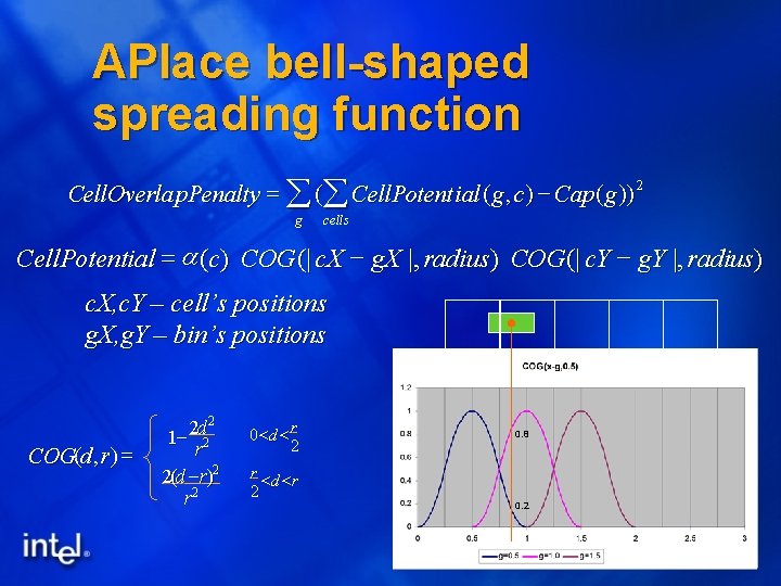
APlace bell-shaped spreading function Cell. Overla p. Penalty = å ( å Cell. Potent ial ( g , c ) - Cap ( g )) 2 g cells Cell. Potential = a (c) COG (| c. X - g. X |, radius) COG (| c. Y - g. Y |, radius) c. X, c. Y – cell’s positions g. X, g. Y – bin’s positions 0. 9 2 COG(d , r) = 1 - 2 d 2 r 2(d -r)2 r 2 0<d < r 2 r <d <r 2 0. 7 0. 8 0. 3 0. 2 SCL Inventing IC design technologies that will be vital to Intel
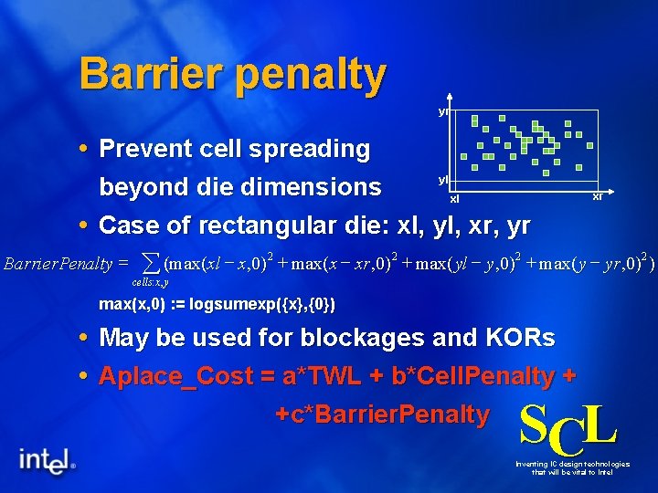
Barrier penalty yr Prevent cell spreading yl beyond die dimensions xl Case of rectangular die: xl, yl, xr, yr Barrier. Penalty = å (max(xl - x, 0) 2 xr + max( x - xr , 0) 2 + max( yl - y, 0) 2 + max( y - yr , 0) 2 ) cells: x , y max(x, 0) : = logsumexp({x}, {0}) May be used for blockages and KORs Aplace_Cost = a*TWL + b*Cell. Penalty + +c*Barrier. Penalty SCL Inventing IC design technologies that will be vital to Intel
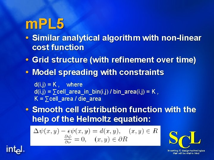
m. PL 5 Similar analytical algorithm with non-linear cost function Grid structure (with refinement over time) Model spreading with constraints d(i, j) = K , where d(i, j) = ∑cell_area_in_bin(i, j) / bin_area(i, j) = K , K = ∑cell_area / die_area Smooth cell distribution function with the help of the Helmoltz equation: SCL Inventing IC design technologies that will be vital to Intel
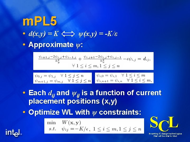
m. PL 5 d(x, y) = K ψ(x, y) = -K/ε Approximate ψ: Each dij and ψij is a function of current placement positions (x, y) Optimize WL with ψ constraints: SCL Inventing IC design technologies that will be vital to Intel
Links http: //www. sigda. org/ispd 2005/contest. htm http: //www. sigda. org/ispd 2006/contest. html http: //www. openedatools. org/projects/oagear http: //www. openedatools. org http: //openeda. si 2. org http: //www. ece. ucsb. edu/~kastner/labyrinth http: //www. staticfreesoft. com http: //www. vlsitechnology. org http: //www. stanford. edu/class/ee 371 http: //embedded. eecs. berkeley. edu/pubs/downloads/sis/in dex. htm http: //www. mcs. anl. gov/tao SCL Inventing IC design technologies that will be vital to Intel
- Slides: 27