RFIC Design and Testing for Wireless Communications A
- Slides: 13

RFIC Design and Testing for Wireless Communications A Praga. TI (TI India Technical University) Course July 18, 21, 22, 2008 Lecture 11: ATE and SOC Testing Vishwani D. Agrawal Foster Dai Auburn University, Dept. of ECE, Auburn, AL 36849, USA 1

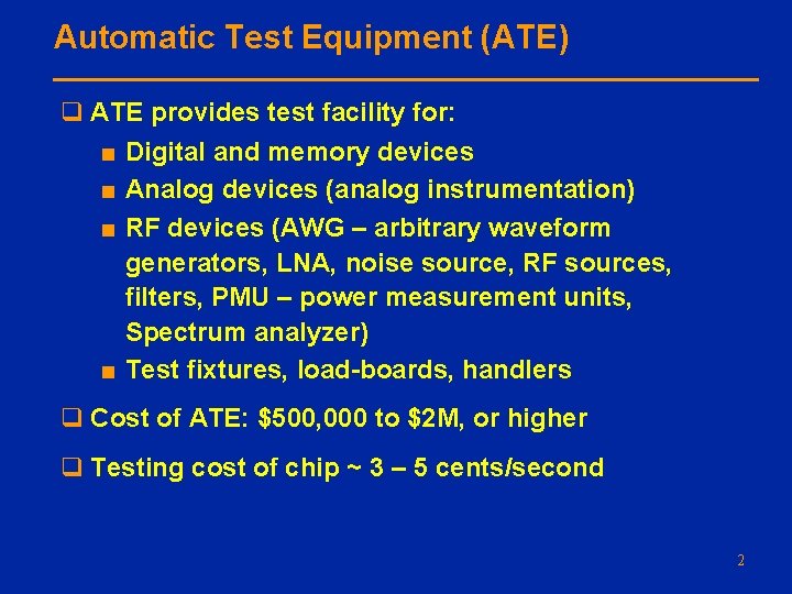
Automatic Test Equipment (ATE) q ATE provides test facility for: ■ Digital and memory devices ■ Analog devices (analog instrumentation) ■ RF devices (AWG – arbitrary waveform generators, LNA, noise source, RF sources, filters, PMU – power measurement units, Spectrum analyzer) ■ Test fixtures, load-boards, handlers q Cost of ATE: $500, 000 to $2 M, or higher q Testing cost of chip ~ 3 – 5 cents/second 2

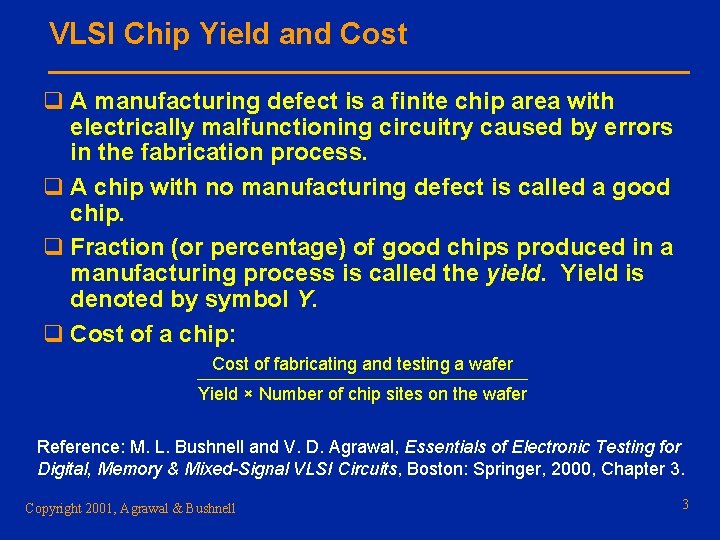
VLSI Chip Yield and Cost q A manufacturing defect is a finite chip area with electrically malfunctioning circuitry caused by errors in the fabrication process. q A chip with no manufacturing defect is called a good chip. q Fraction (or percentage) of good chips produced in a manufacturing process is called the yield. Yield is denoted by symbol Y. q Cost of a chip: Cost of fabricating and testing a wafer ───────────── Yield × Number of chip sites on the wafer Reference: M. L. Bushnell and V. D. Agrawal, Essentials of Electronic Testing for Digital, Memory & Mixed-Signal VLSI Circuits, Boston: Springer, 2000, Chapter 3. Copyright 2001, Agrawal & Bushnell 3

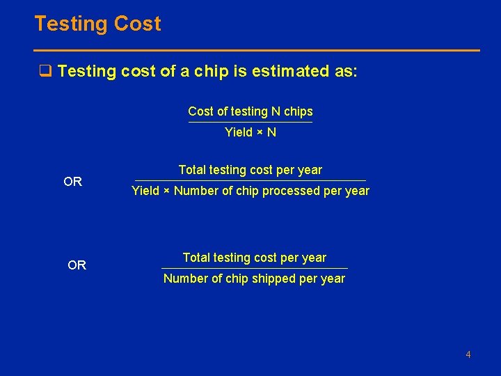
Testing Cost q Testing cost of a chip is estimated as: Cost of testing N chips ─────── Yield × N OR OR Total testing cost per year ───────────── Yield × Number of chip processed per year Total testing cost per year ─────────── Number of chip shipped per year 4

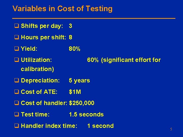
Variables in Cost of Testing q Shifts per day: 3 q Hours per shift: 8 q Yield: 80% q Utilization: calibration) 60% (significant effort for q Depreciation: 5 years q Cost of ATE: $1 M q Cost of handler: $250, 000 q Test time: 1. 5 seconds q Handler index time: 1 second 5

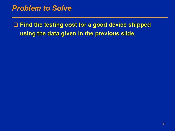
Problem to Solve q Find the testing cost for a good device shipped using the data given in the previous slide. 6

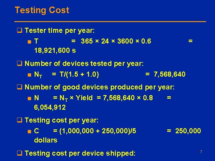
Testing Cost q Tester time per year: ■T = 365 × 24 × 3600 × 0. 6 18, 921, 600 s = q Number of devices tested per year: ■ NT = T/(1. 5 + 1. 0) = 7, 568, 640 q Number of good devices produced per year: ■N = NT × Yield = 7, 568, 640 × 0. 8 = 6, 054, 912 q Testing cost per year: ■C = (1, 000 + 250, 000)/5 dollars = 250, 000 q Testing cost per device shipped: 7

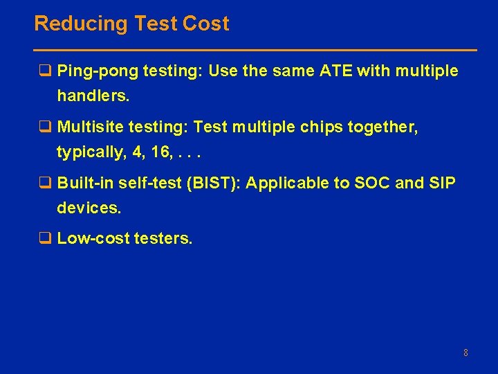
Reducing Test Cost q Ping-pong testing: Use the same ATE with multiple handlers. q Multisite testing: Test multiple chips together, typically, 4, 16, . . . q Built-in self-test (BIST): Applicable to SOC and SIP devices. q Low-cost testers. 8

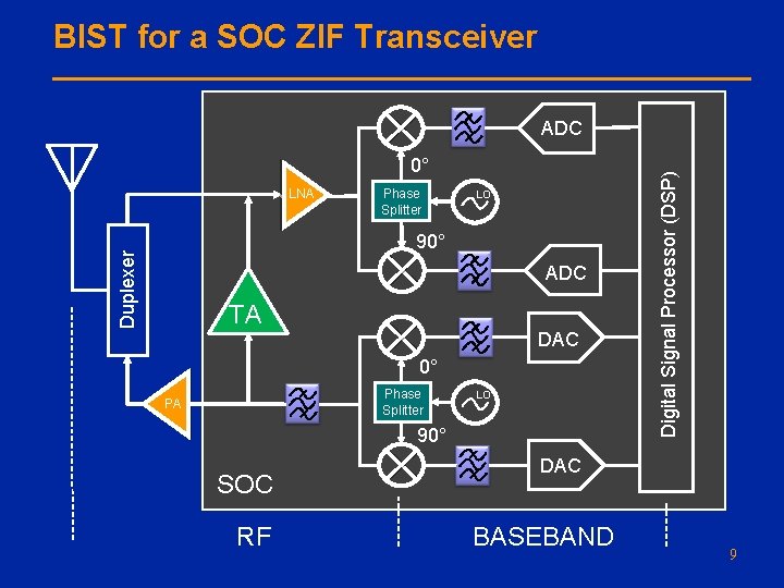
BIST for a SOC ZIF Transceiver 0° LNA Phase Splitter LO Duplexer 90° ADC TA DAC 0° Phase Splitter PA LO 90° SOC RF Digital Signal Processor (DSP) ADC DAC BASEBAND 9

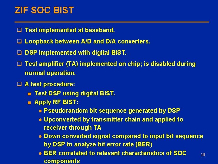
ZIF SOC BIST q Test implemented at baseband. q Loopback between A/D and D/A converters. q DSP implemented with digital BIST. q Test amplifier (TA) implemented on chip; is disabled during normal operation. q A test procedure: ■ Test DSP using digital BIST. ■ Apply RF BIST: ● Pseudorandom bit sequence generated by DSP ● Upconverted by transmitter chain and applied to receiver through TA ● Down converted signal compared to input bit sequence by DSP to analyze bit error rate (BER) ● BER correlated to relevant characteristics of SOC 10 components

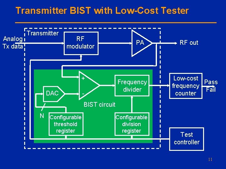
Transmitter BIST with Low-Cost Tester Analog Tx data Transmitter RF modulator + DAC - PA Frequency divider RF out Low-cost Pass frequency Fail counter BIST circuit N Configurable threshold register Configurable division register Test controller 11

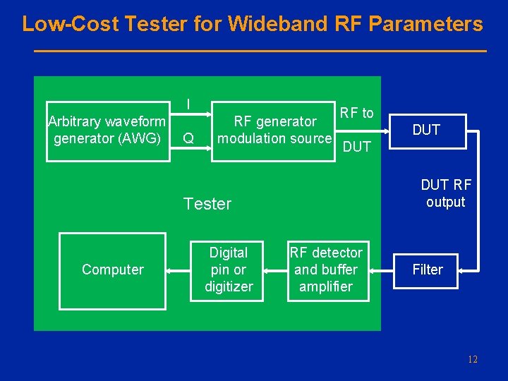
Low-Cost Tester for Wideband RF Parameters I Arbitrary waveform generator (AWG) Q RF generator modulation source RF to DUT DUT RF output Tester Computer Digital pin or digitizer RF detector and buffer amplifier Filter 12

References q SOC BIST ■ J. Dabrowski, “Bi. ST Model for IC RF-Transceiver Front. End, ” Proc. 18 th IEEE International Symp. on Defect and Fault Tolerance in VLSI Systems, 2003. ■ D. Lupea, et al. , “RF-BIST: Loopback Spectral Signature Analysis, ” Proc. Design, Automation and Test in Europe Conf. , 2003. q BIST for power amplifier ■ F. Obaldia, et al. , “On-Chip Test Mechanism for Transceiver Power Amplifier and Oscillator Frequency, ” US Patent No. 20040148121 A 1, 2004. q Low-cost testing ■ F. Goh, et al. , “Innovative Technique for Testing Wide Bandwidth Frequency Response, ” Wireless Broadband Forum, Cambridge, UK, 2004. 13