RFIC Design and Testing for Wireless Communications A
- Slides: 28

RFIC Design and Testing for Wireless Communications A Praga. TI (TI India Technical University) Course July 18, 21, 22, 2008 Lecture 2: Power and Gain Measurement Vishwani D. Agrawal Foster Dai Auburn University, Dept. of ECE, Auburn, AL 36849, USA 1

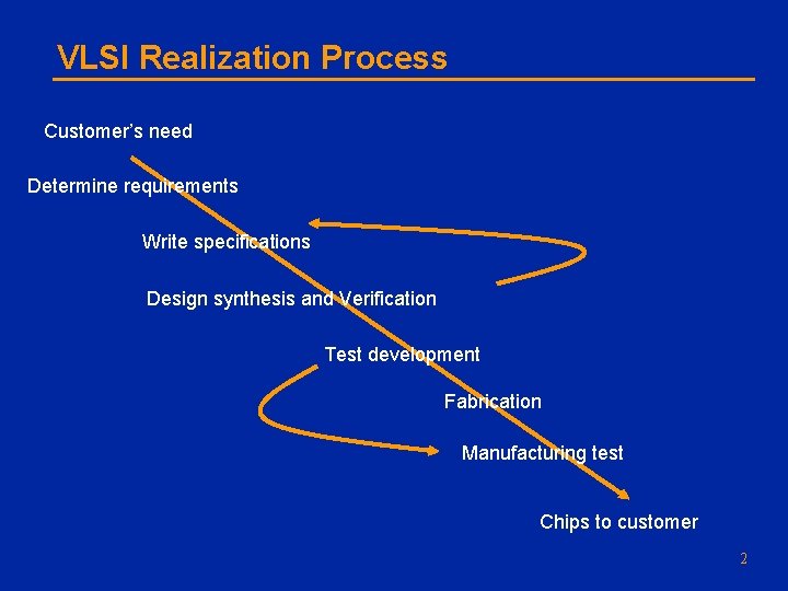
VLSI Realization Process Customer’s need Determine requirements Write specifications Design synthesis and Verification Test development Fabrication Manufacturing test Chips to customer 2

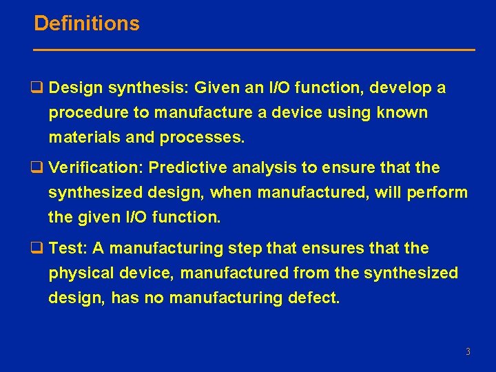
Definitions q Design synthesis: Given an I/O function, develop a procedure to manufacture a device using known materials and processes. q Verification: Predictive analysis to ensure that the synthesized design, when manufactured, will perform the given I/O function. q Test: A manufacturing step that ensures that the physical device, manufactured from the synthesized design, has no manufacturing defect. 3

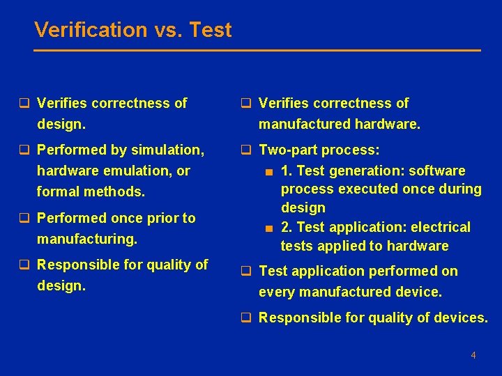
Verification vs. Test q Verifies correctness of design. q Verifies correctness of manufactured hardware. q Performed by simulation, hardware emulation, or formal methods. q Performed once prior to manufacturing. q Two-part process: ■ 1. Test generation: software process executed once during design ■ 2. Test application: electrical tests applied to hardware q Responsible for quality of design. q Test application performed on every manufactured device. q Responsible for quality of devices. 4

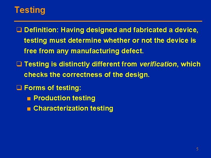
Testing q Definition: Having designed and fabricated a device, testing must determine whether or not the device is free from any manufacturing defect. q Testing is distinctly different from verification, which checks the correctness of the design. q Forms of testing: ■ Production testing ■ Characterization testing 5

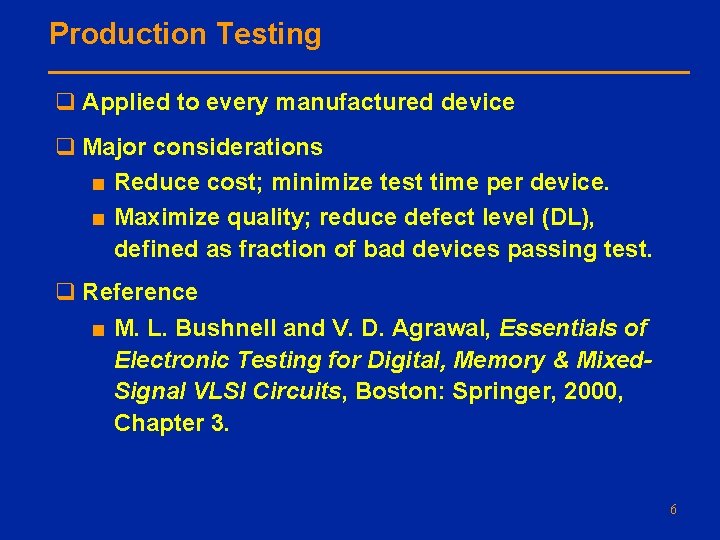
Production Testing q Applied to every manufactured device q Major considerations ■ Reduce cost; minimize test time per device. ■ Maximize quality; reduce defect level (DL), defined as fraction of bad devices passing test. q Reference ■ M. L. Bushnell and V. D. Agrawal, Essentials of Electronic Testing for Digital, Memory & Mixed. Signal VLSI Circuits, Boston: Springer, 2000, Chapter 3. 6

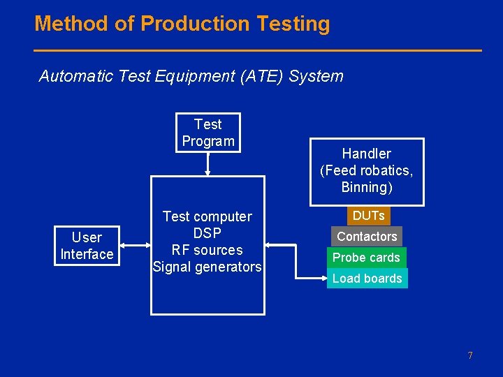
Method of Production Testing Automatic Test Equipment (ATE) System Test Program User Interface Test computer DSP RF sources Signal generators Handler (Feed robatics, Binning) DUTs Contactors Probe cards Load boards 7

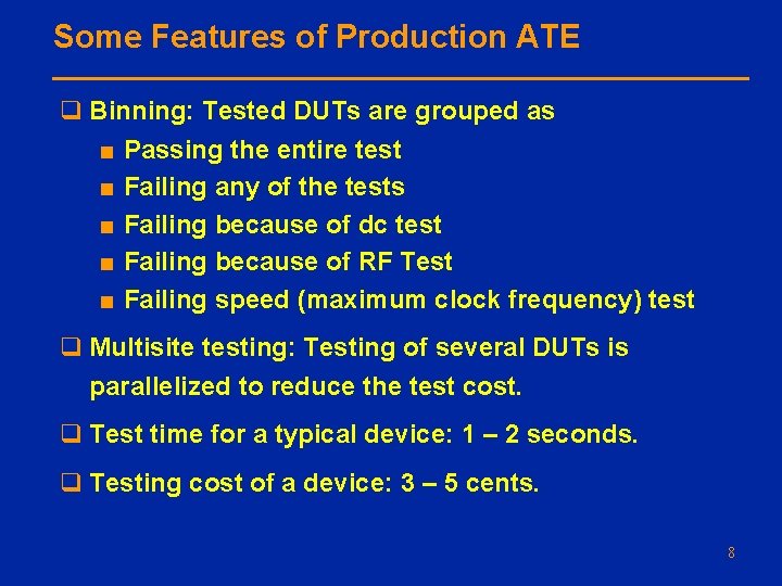
Some Features of Production ATE q Binning: Tested DUTs are grouped as ■ Passing the entire test ■ Failing any of the tests ■ Failing because of dc test ■ Failing because of RF Test ■ Failing speed (maximum clock frequency) test q Multisite testing: Testing of several DUTs is parallelized to reduce the test cost. q Test time for a typical device: 1 – 2 seconds. q Testing cost of a device: 3 – 5 cents. 8

Characterization Testing q Performed at the beginning of production phase. q Objective: To verify the design, manufacturability, and test program. q Method: ■ Few devices tested very thoroughly ■ Failures are often diagnosed ■ Tests are more elaborate than the production tests ■ Test time (and testing cost) not a consideration ■ Test program is verified and corrected in necessary ■ ATE system and additional laboratory setup may 9 be used

RF Tests q Basic tests ■ Scattering parameters (S-parameters) ■ Frequency and gain measurements ■ Power efficiency measurements q Distortion measurements q Noise measurements 10

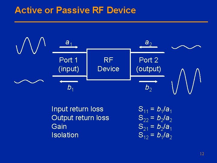
Scattering Parameters (S-Parameters) q An RF function is a two-port device with ■ Characteristic impedance (Z 0): ● Z 0 = 50Ω for wireless communications devices ● Z 0 = 75Ω for cable TV devices ■ Gain and frequency characteristics q S-Parameters of an RF device ■ S 11 : input return loss or input reflection coefficient ■ S 22 : output return loss or output reflection coefficient ■ S 21 : gain or forward transmission coefficient ■ S 12 : isolation or reverse transmission coefficient q S-Parameters are complex numbers and can be 11

Active or Passive RF Device a 1 Port 1 (input) a 2 RF Device b 1 Input return loss Output return loss Gain Isolation Port 2 (output) b 2 S 11 = b 1/a 1 S 22 = b 2/a 2 S 21 = b 2/a 1 S 12 = b 1/a 2 12

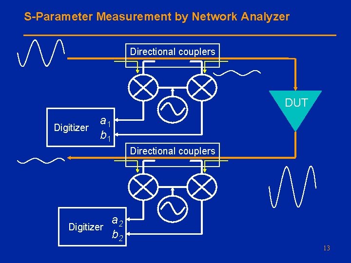
S-Parameter Measurement by Network Analyzer Directional couplers DUT a 1 Digitizer b 1 Directional couplers a 2 Digitizer b 2 13

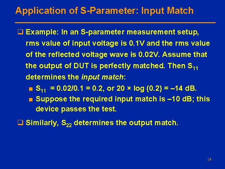
Application of S-Parameter: Input Match q Example: In an S-parameter measurement setup, rms value of input voltage is 0. 1 V and the rms value of the reflected voltage wave is 0. 02 V. Assume that the output of DUT is perfectly matched. Then S 11 determines the input match: ■ S 11 = 0. 02/0. 1 = 0. 2, or 20 × log (0. 2) = – 14 d. B. ■ Suppose the required input match is – 10 d. B; this device passes the test. q Similarly, S 22 determines the output match. 14

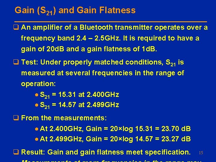
Gain (S 21) and Gain Flatness q An amplifier of a Bluetooth transmitter operates over a frequency band 2. 4 – 2. 5 GHz. It is required to have a gain of 20 d. B and a gain flatness of 1 d. B. q Test: Under properly matched conditions, S 21 is measured at several frequencies in the range of operation: ● S 21 = 15. 31 at 2. 400 GHz ● S 21 = 14. 57 at 2. 499 GHz q From the measurements: ● At 2. 400 GHz, Gain = 20×log 15. 31 = 23. 70 d. B ● At 2. 499 GHz, Gain = 20×log 14. 57 = 23. 27 d. B q Result: Gain and gain flatness meet specification. 15

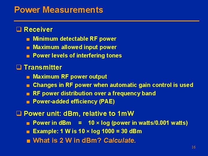
Power Measurements q Receiver ■ Minimum detectable RF power ■ Maximum allowed input power ■ Power levels of interfering tones q Transmitter ■ ■ Maximum RF power output Changes in RF power when automatic gain control is used RF power distribution over a frequency band Power-added efficiency (PAE) q Power unit: d. Bm, relative to 1 m. W ■ Power in d. Bm = 10 × log (power in watts/0. 001 watts) ■ Example: 1 W is 10 × log 1000 = 30 d. Bm ■ What is 2 W in d. Bm? Calculate. 16

Power Spectrum Measurements q Spur measurement q Harmonic measurement q Adjacent channel interference 17

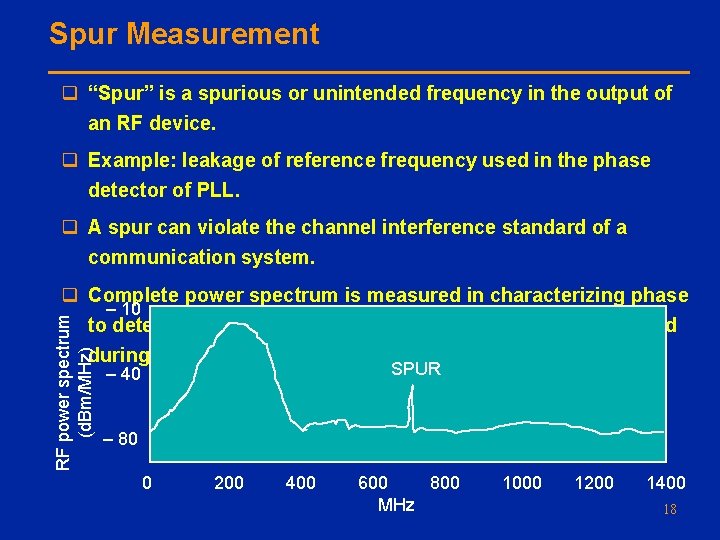
Spur Measurement q “Spur” is a spurious or unintended frequency in the output of an RF device. q Example: leakage of reference frequency used in the phase detector of PLL. q A spur can violate the channel interference standard of a communication system. RF power spectrum (d. Bm/MHz) q Complete power spectrum is measured in characterizing phase – 10 to determine which interfering frequencies should be checked during production testing. SPUR – 40 – 80 0 200 400 600 800 MHz 1000 1200 1400 18

Harmonic Measurements q Multiples of the carrier frequency are called harmonics. q Harmonics are generated due to ■ nonlinearity in semiconductor devices ■ clipping (saturation) in amplifiers. q Harmonics may interfere with other signals and must be measured to verify that a manufactured device meets the specification. 19

Adjacent Channel Power Ratio (ACPR) q Ratio of average power in the adjacent frequency channel to the average power in the transmitted frequency channel. q Also known as adjacent channel leakage ratio (ACLR). q A measure of transmitter performance. 20

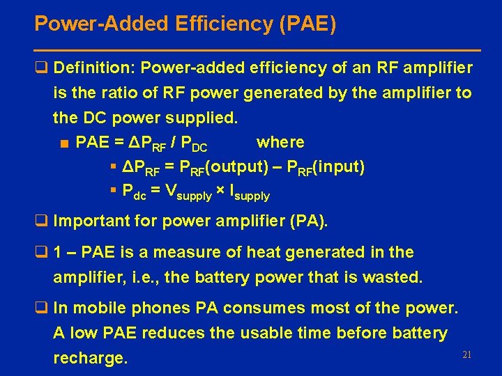
Power-Added Efficiency (PAE) q Definition: Power-added efficiency of an RF amplifier is the ratio of RF power generated by the amplifier to the DC power supplied. ■ PAE = ΔPRF / PDC where § ΔPRF = PRF(output) – PRF(input) § Pdc = Vsupply × Isupply q Important for power amplifier (PA). q 1 – PAE is a measure of heat generated in the amplifier, i. e. , the battery power that is wasted. q In mobile phones PA consumes most of the power. A low PAE reduces the usable time before battery 21 recharge.

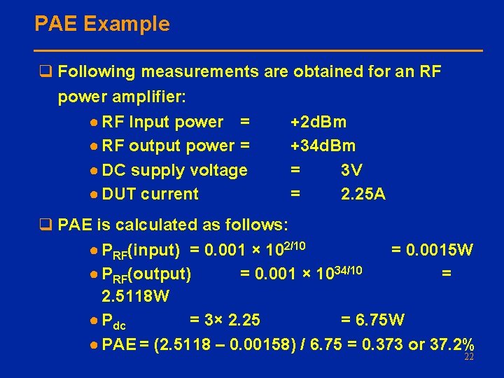
PAE Example q Following measurements are obtained for an RF power amplifier: ● RF Input power = +2 d. Bm ● RF output power = +34 d. Bm ● DC supply voltage = 3 V ● DUT current = 2. 25 A q PAE is calculated as follows: ● PRF(input) = 0. 001 × 102/10 = 0. 0015 W ● PRF(output) = 0. 001 × 1034/10 = 2. 5118 W ● Pdc = 3× 2. 25 = 6. 75 W ● PAE = (2. 5118 – 0. 00158) / 6. 75 = 0. 373 or 37. 2% 22

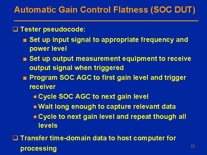
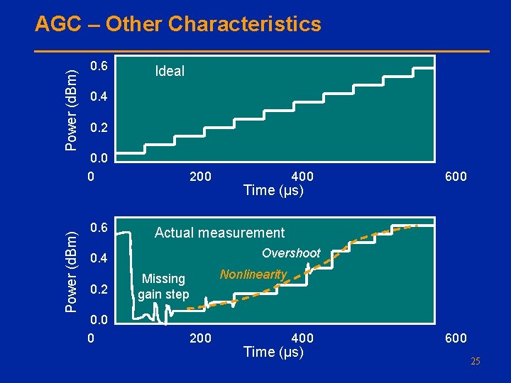
Automatic Gain Control Flatness (SOC DUT) q Tester pseudocode: ■ Set up input signal to appropriate frequency and power level ■ Set up output measurement equipment to receive output signal when triggered ■ Program SOC AGC to first gain level and trigger receiver ● Cycle SOC AGC to next gain level ● Wait long enough to capture relevant data ● Cycle to next gain level and repeat though all levels q Transfer time-domain data to host computer for processing 23

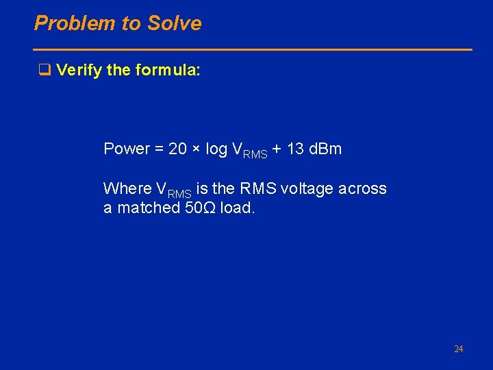
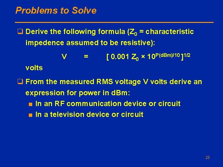
Problem to Solve q Verify the formula: Power = 20 × log VRMS + 13 d. Bm Where VRMS is the RMS voltage across a matched 50Ω load. 24

Power (d. Bm) AGC – Other Characteristics 0. 6 Ideal 0. 4 0. 2 0. 0 0 0. 6 200 0. 0 0 Time (μs) 600 Actual measurement Overshoot 0. 4 0. 2 400 Nonlinearity Missing gain step 200 400 Time (μs) 600 25

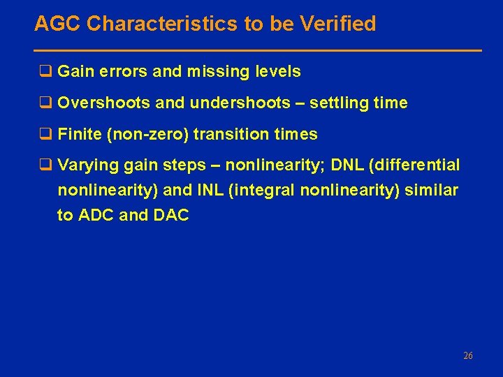
AGC Characteristics to be Verified q Gain errors and missing levels q Overshoots and undershoots – settling time q Finite (non-zero) transition times q Varying gain steps – nonlinearity; DNL (differential nonlinearity) and INL (integral nonlinearity) similar to ADC and DAC 26

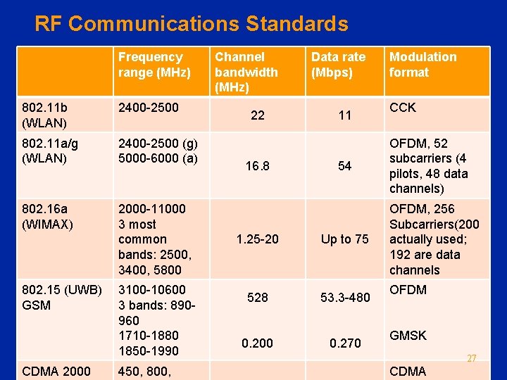
RF Communications Standards Frequency range (MHz) 802. 11 b (WLAN) 2400 -2500 802. 11 a/g (WLAN) 2400 -2500 (g) 5000 -6000 (a) 802. 16 a (WIMAX) 2000 -11000 3 most common bands: 2500, 3400, 5800 802. 15 (UWB) GSM CDMA 2000 3100 -10600 3 bands: 890960 1710 -1880 1850 -1990 450, 800, Channel bandwidth (MHz) 22 16. 8 Data rate (Mbps) 11 54 1. 25 -20 Up to 75 528 53. 3 -480 0. 200 0. 270 Modulation format CCK OFDM, 52 subcarriers (4 pilots, 48 data channels) OFDM, 256 Subcarriers(200 actually used; 192 are data channels OFDM GMSK 27 CDMA

Problems to Solve q Derive the following formula (Z 0 = characteristic impedence assumed to be resistive): V = [ 0. 001 Z 0 × 10 P(d. Bm)/10 ]1/2 volts q From the measured RMS voltage V volts derive an expression for power in d. Bm: ■ In an RF communication device or circuit ■ In a television device or circuit 28