RF Systems Oscillators Ring Oscillator Random Simulation LC
- Slides: 21

RF Systems Oscillators • Ring Oscillator • Random Simulation • LC Oscillator • Voltage Controlled Oscillator • High performance VCO • Targil 3: Differential VCO or Relaxation Oscillator The role of oscillators is to create a periodic logic or analog signal with a stable and predictable frequency. Oscillators are required to generate the carrying signals for radio frequency transmission, but also the main clocks of processors. .

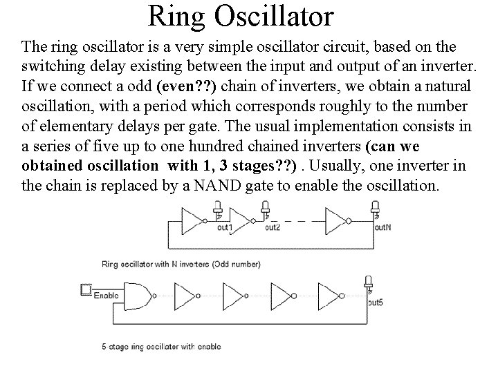
Ring Oscillator The ring oscillator is a very simple oscillator circuit, based on the switching delay existing between the input and output of an inverter. If we connect a odd (even? ? ) chain of inverters, we obtain a natural oscillation, with a period which corresponds roughly to the number of elementary delays per gate. The usual implementation consists in a series of five up to one hundred chained inverters (can we obtained oscillation with 1, 3 stages? ? ). Usually, one inverter in the chain is replaced by a NAND gate to enable the oscillation.

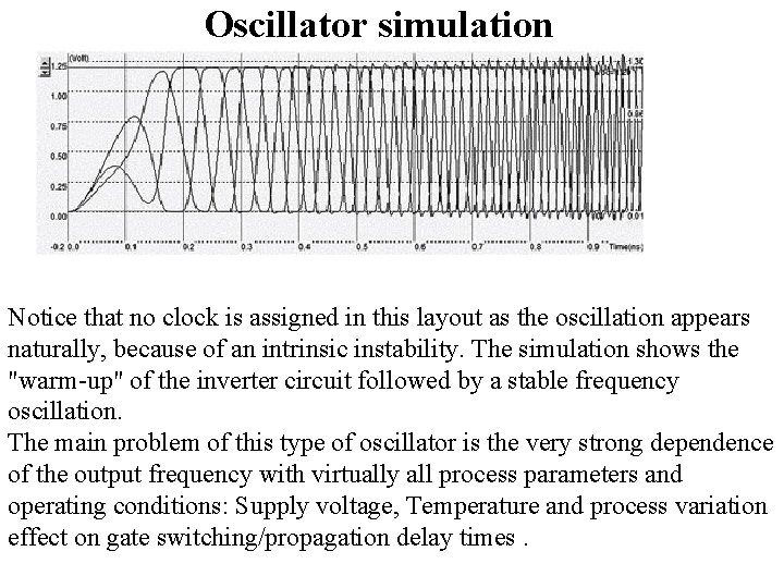
Oscillator simulation Notice that no clock is assigned in this layout as the oscillation appears naturally, because of an intrinsic instability. The simulation shows the "warm-up" of the inverter circuit followed by a stable frequency oscillation. The main problem of this type of oscillator is the very strong dependence of the output frequency with virtually all process parameters and operating conditions: Supply voltage, Temperature and process variation effect on gate switching/propagation delay times.

Oscillator simulation As an example, the power supply voltage VDD has a very significant importance on the oscillating frequency. This dependency can be analyzed using the parametric analysis in the Analysis menu. Several simulations are performed with VDD varying from 0. 8 V to 1. 4 V with a 50 m. V step (Test in simulation). We clearly observe a very important increase of the output frequency with VDD (Almost a factor of 2 between the lower and upper bounds). This means that any supply fluctuation has a significant impact on the oscillator frequency. The oscillation frequency of the ring oscillator is not stable, not controllable, and somehow not precisely predictable, as it is based on the switching characteristics of logic gates, which may fluctuate +/20%. As a conclusion, ring oscillators have poor performances, and may only be used in low performance clocking systems, or for a dynamic characterization of the technology.

Random Simulation A Monte Carlo analysis usually has to be performed to observe the technology variation influence on the oscillator frequency. The basic principles of this analysis is to sort in a random way a set of technological parameters, and conduct for each random set the complete analog simulation. Each point in the X axis corresponds to one simulation, with a specific set of parameters. There is no correlation between adjacent points, because of the random nature of each simulation conditions. We observe again the significant fluctuation of the oscillator frequency. In many simulators the threshold and mobility parameters are varying with a Normal distribution, with a typical variation of 10%. The normal distribution of the threshold voltage Vt corresponds to a density of probability following the following equation. The aspect of f versus Vt is also demonstrated.

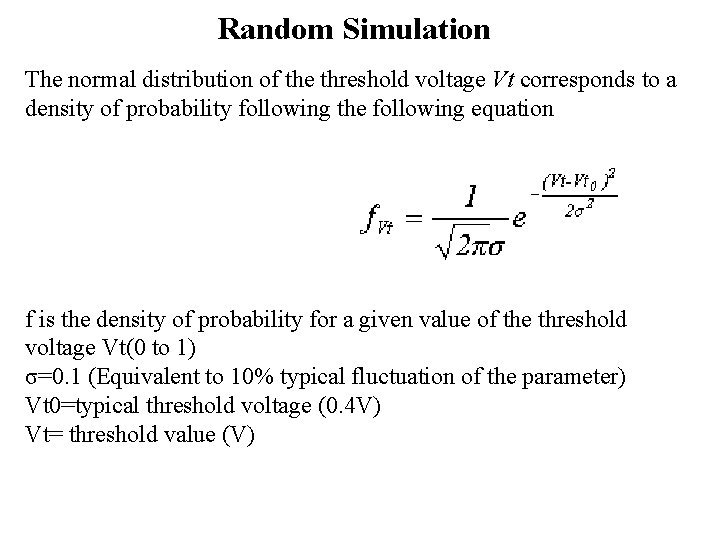
Random Simulation The normal distribution of the threshold voltage Vt corresponds to a density of probability following the following equation f is the density of probability for a given value of the threshold voltage Vt(0 to 1) σ=0. 1 (Equivalent to 10% typical fluctuation of the parameter) Vt 0=typical threshold voltage (0. 4 V) Vt= threshold value (V)

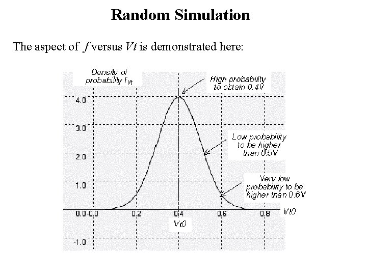
Random Simulation The aspect of f versus Vt is demonstrated here:

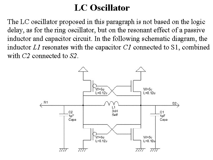
LC Oscillator The LC oscillator proposed in this paragraph is not based on the logic delay, as for the ring oscillator, but on the resonant effect of a passive inductor and capacitor circuit. In the following schematic diagram, the inductor L 1 resonates with the capacitor C 1 connected to S 1, combined with C 2 connected to S 2.

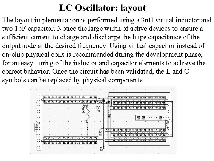
LC Oscillator: layout The layout implementation is performed using a 3 n. H virtual inductor and two 1 p. F capacitor. Notice the large width of active devices to ensure a sufficient current to charge and discharge the huge capacitance of the output node at the desired frequency. Using virtual capacitor instead of on-chip physical coils is recommended during the development phase, for an easy tuning of the inductor and capacitor elements to achieve the correct behavior. Once the circuit has been validated, the L and C symbols can be replaced by physical components.

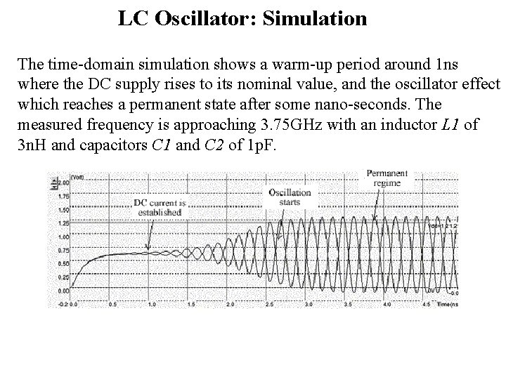
LC Oscillator: Simulation The time-domain simulation shows a warm-up period around 1 ns where the DC supply rises to its nominal value, and the oscillator effect which reaches a permanent state after some nano-seconds. The measured frequency is approaching 3. 75 GHz with an inductor L 1 of 3 n. H and capacitors C 1 and C 2 of 1 p. F.

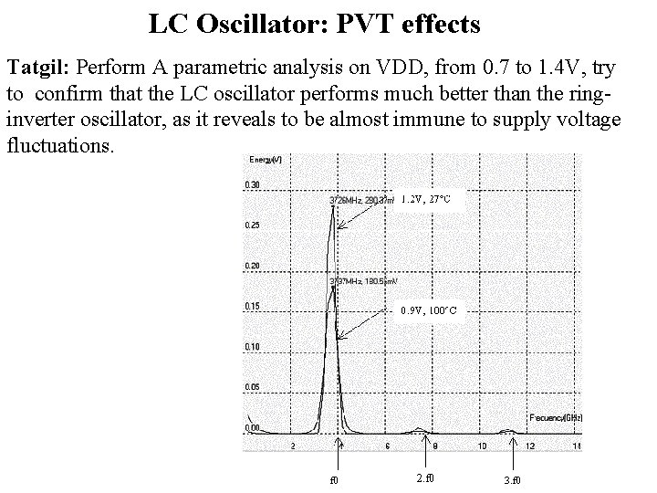
LC Oscillator: Simulation The Fourier transform of the output s 1 reveals a main sinusoidal contribution at f 0=3. 725 GHz as expected, and some harmonic contains at 2. f 0 and 3 f 0. The remarkable property of this circuit is its ability to remain in a stable frequency even if we change the supply voltage or the temperature, which features a significant improvement as compared to the ring oscillator. Furthermore, the variation of the MOS model parameters have almost no effect on the frequency. We investigate the effect of VDD on the resonating frequency by lowering manually VDD from 1. 2 V down to 0. 9 V. The result is a significant increase of the warm-up phase, while the final oscillation frequency remains unchanged.

LC Oscillator: PVT effects Tatgil: Perform A parametric analysis on VDD, from 0. 7 to 1. 4 V, try to confirm that the LC oscillator performs much better than the ringinverter oscillator, as it reveals to be almost immune to supply voltage fluctuations.

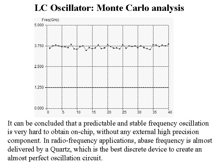
LC Oscillator: PVT effects Tatgil: Perform A parametric analysis on VDD, from 0. 7 to 1. 4 V, try to confirm that the LC oscillator performs much better than the ringinverter oscillator, as it reveals to be almost immune to supply voltage fluctuations. Unfortunately, the inductance of an on-chip coil is not perfectly constant, as the material resistance, conductor width and oxide thickness may vary several %. The capacitance of a poly/poly 2 structure, used for implementing the passive capacitor, may also vary due to the process fluctuation impact on the inter-layer oxide. The temperature also has an influence on the capacitance value. the Montecarlo simulation mode also impacts the value of all virtual elements in a similar way as for the threshold voltage and the mobility: before the simulation starts, the L and C values are assigned a value that fluctuates +/-10% with a normal distribution around the user-defined impedance. The result is a significant variation of the oscillator frequency with the process parameters.

LC Oscillator: Monte Carlo analysis It can be concluded that a predictable and stable frequency oscillation is very hard to obtain on-chip, without any external high precision component. In radio-frequency applications, abase frequency is almost delivered by a Quartz, which is the best discrete device to create an almost perfect oscillation circuit.

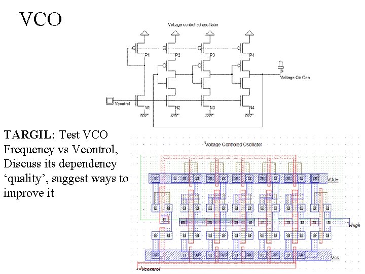
Voltage Controlled Oscillator The voltage controlled oscillator (VCO) generates a clock with a controllable frequency. The VCO is commonly used for clock generation in phase lock loop circuits, as described later in this chapter. The clock may vary typically +/-50% of its central frequency. A current-starved voltage controlled oscillator is shown here. The current-starved inverter chain uses a voltage control Vcontrol to modify the current that flows in the N 1, P 1 branch. The current through N 1 is mirrored by N 2, N 3 and N 4. The same current flows in P 1. The current through P 1 is mirrored by P 2, P 2, and P 4. Consequently, the change in Vcontrol induces a global change in the inverter currents, and directly acts on the delay. A higher odd number of stages is commonly implemented, depending on the target oscillating frequency and consumption constraints. The implementation of the current-starved VCO for a 5 -inverter chain is given here. The current mirror is situated on the left. Five inverters have been designed to create the basic ring oscillator. Then a buffer inverter is situated on the right side of the layout.

VCO TARGIL: Test VCO Frequency vs Vcontrol, Discuss its dependency ‘quality’, suggest ways to improve it

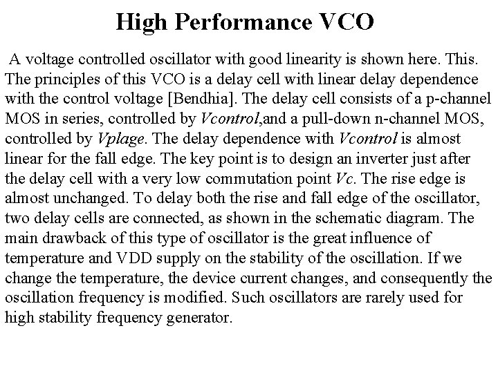
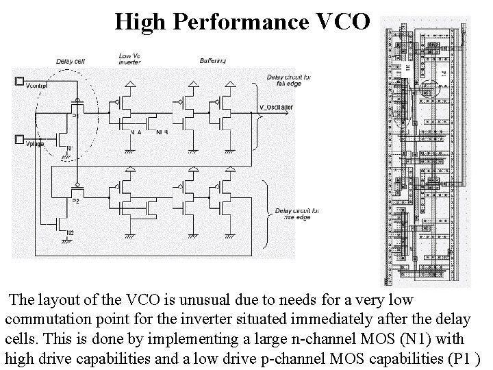
High Performance VCO A voltage controlled oscillator with good linearity is shown here. This. The principles of this VCO is a delay cell with linear delay dependence with the control voltage [Bendhia]. The delay cell consists of a p-channel MOS in series, controlled by Vcontrol, and a pull-down n-channel MOS, controlled by Vplage. The delay dependence with Vcontrol is almost linear for the fall edge. The key point is to design an inverter just after the delay cell with a very low commutation point Vc. The rise edge is almost unchanged. To delay both the rise and fall edge of the oscillator, two delay cells are connected, as shown in the schematic diagram. The main drawback of this type of oscillator is the great influence of temperature and VDD supply on the stability of the oscillation. If we change the temperature, the device current changes, and consequently the oscillation frequency is modified. Such oscillators are rarely used for high stability frequency generator.

High Performance VCO The layout of the VCO is unusual due to needs for a very low commutation point for the inverter situated immediately after the delay cells. This is done by implementing a large n-channel MOS (N 1) with high drive capabilities and a low drive p-channel MOS capabilities (P 1 )

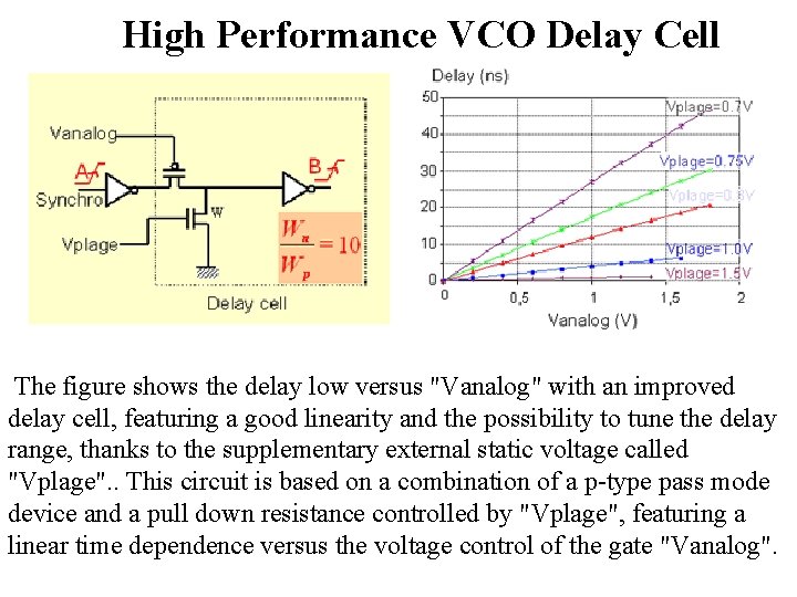
High Performance VCO Delay Cell The figure shows the delay low versus "Vanalog" with an improved delay cell, featuring a good linearity and the possibility to tune the delay range, thanks to the supplementary external static voltage called "Vplage". . This circuit is based on a combination of a p-type pass mode device and a pull down resistance controlled by "Vplage", featuring a linear time dependence versus the voltage control of the gate "Vanalog".

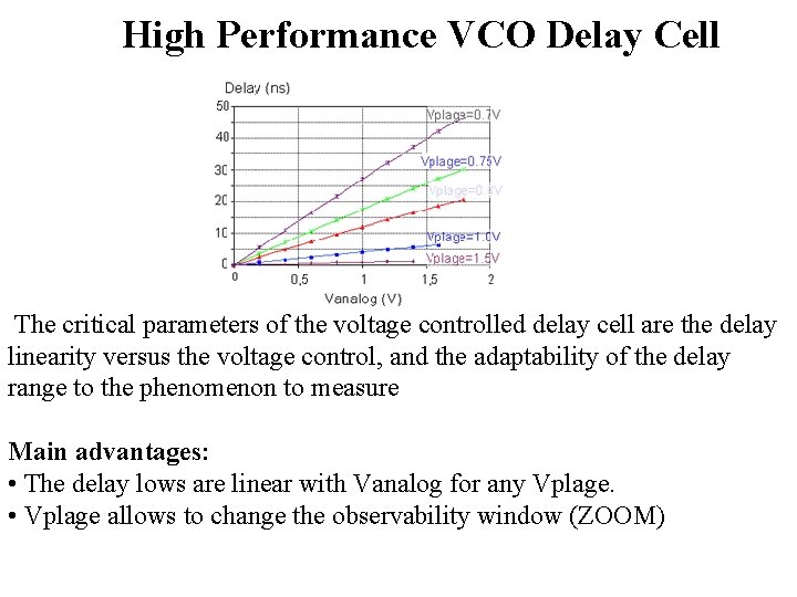
High Performance VCO Delay Cell The critical parameters of the voltage controlled delay cell are the delay linearity versus the voltage control, and the adaptability of the delay range to the phenomenon to measure Main advantages: • The delay lows are linear with Vanalog for any Vplage. • Vplage allows to change the observability window (ZOOM)

Targil 3 ØDesign Fully differential ICO for 100 MHz oscillation, minimize its dependency on PVT to lower than 20% by temperature current compensation and/or regulated voltage stabilization and/or vt compensation. Ø Design Relaxation oscillator with ‘real’ current sources, FF’s and Comparator, evaluate its center frequency sensitivity to PVT