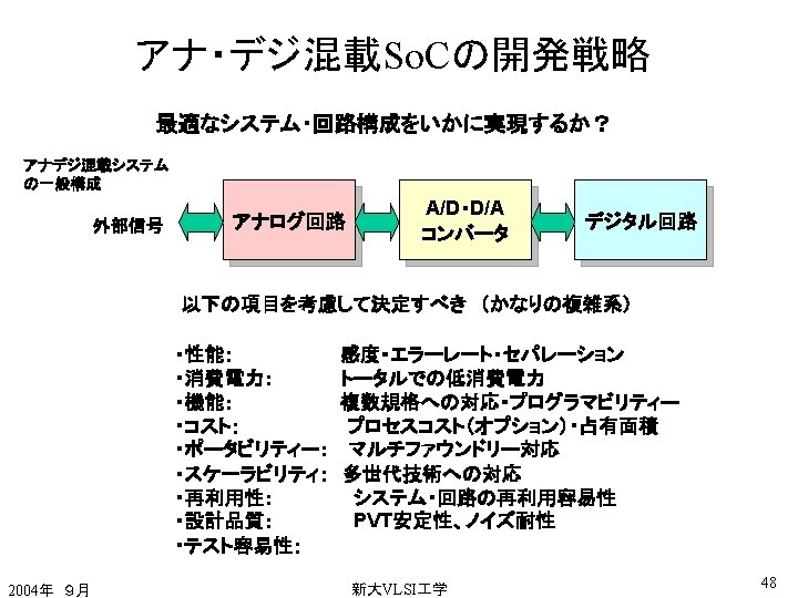
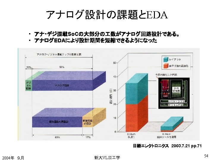
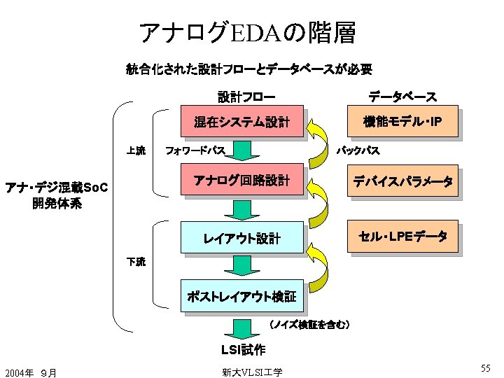
RF IEEE 1394 USB Blue tooth Wireless LAN

デジタルネットワーク社会 デジタルネットワーク化も現在の特徴である。ここでもアナログ・RF混載技術が使われる IEEE 1394, USB, Blue tooth, Wireless LAN DAB CS/BS Ethenet Digital TV ITS HII Station Home network ADSL, FTTH Network Digital TV W-CDMA 2004年 9月 Home Server DVC 新大VLSI 学 DVD 5

有線ネットワークシステムの構成:2 ケーブル用超高速シリアルI/F 光インターフェースを基本として プリエンファシスや簡単なアナログイコライザーを加えている。 Parallel Data In Ref. Clk D P/S Clock Multiplier Unit (CMU) Kd PD MUX CP S/P Serial Out Input Buffer Serial In Tone Sig. Gen. Parallel Data Out 2004年 9月 + + + Driver Clock Recovery Unit (CRU) VCO LPF Kp Tone_Out 新大VLSI 学 8

有線ネットワークシステムの構成: 3 Gb Ethernet の例: デジタル信号処理技術の導入 デジタル信号処理の導入により高度な処理が可能 ・デジタルイコライザー ・エコーキャンセラー ・クロストークキャンセラー ・高度なプリエンファシス ただし、超高速ADC, DAC, ロジック回路が必要 DAC DAC Pulse Shaping Line I/F TX 1 TX 2 TX 3 TX 4 ADC 250 Mbaud ADC (PAM-5) FFE Clock Recovery Slicer DFE Side-stream Scrambler & Trellis, Viterbi Symbol Encoder Side-stream Descrambler & Trellis, Viterbi decoder Echo Canceller 3 -NEXTCanceller 2004年 9月 新大VLSI 学 9
 690 Mbps PCI 1. 06 Gbps (Parallel) SCSI (Parallel) 1394")
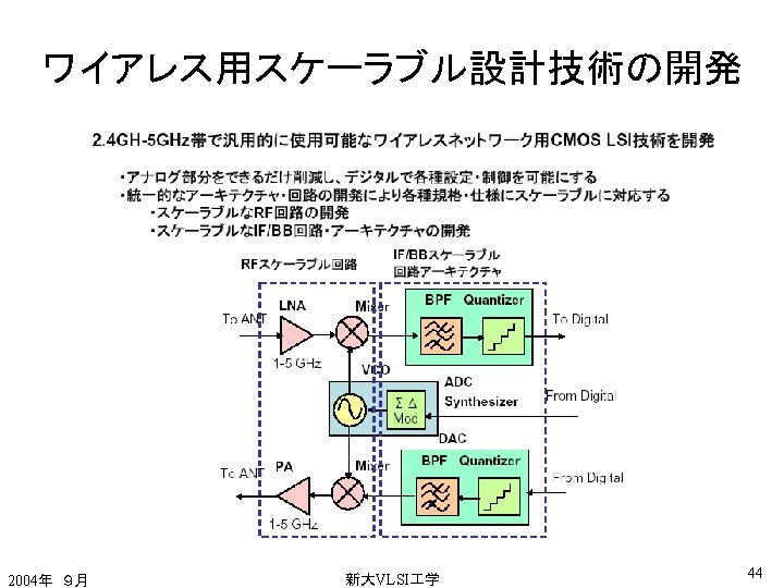
高速I/Fのロードマップ 身近な分野でも数Gbpsの信号伝送は当たりまえになっている Display (Parallel) 690 Mbps PCI 1. 06 Gbps (Parallel) SCSI (Parallel) 1394 (Serial) Year 2004年 9月 SVGA (800 x 600) 1. 36 Gbps XGA (1024 x 768) 2. 11 Gbps 2. 26 Gbps 3. 3 Gbps SXGA (1280 x 1024) UXGA (1600 x 1200) 4. 22 Gbps 8. 45 Gbps? 32 bit@33 MHz 32 bit@66 MHz 64 bit@132 MHz? 32 bit@132 MHz 320 Mbps 640 Mbps Ultra-SCSI Ultra-2 200 Mbps 400 Mbps 1394. a 1998 1999 1. 28 Gbps 2. 56 Gbps? 5. 12 Gbps? Ultra-4 ? Ultra-5 ? 1. 60 Gbps 800 Mbps 1394. b 3. 20 Gbps Ultra-3 2000 新大VLSI 学 2001 2002 11
, Processing : WS (MIPS) 処理速度・伝送速度の進展はムーアの法則をしのいでいる。 5000 2000 1000 WS 2")
処理速度・伝送速度の加速 Data rate (Mbaud), Processing : WS (MIPS) 処理速度・伝送速度の進展はムーアの法則をしのいでいる。 5000 2000 1000 WS 2 x/1. 5 year 500 1000 BT “Moore’s Law” 200 1394 100 BT “Super Moore’s law” 2 x/0. 6 year 50 20 10 USB Ethernet 10 BT 5. 0 ’ 88 ~’ 89 2004年 9月 ’ 90 ~ ’ 91 ’ 92 ~ ’ 93 ’ 94 ~ ’ 95 ’ 96 ~ ’ 97 新大VLSI 学 ’ 98 ~ ’ 99 ’ 00 ~ ’ 01 12
 ・デジタル記録(HDD, DVCなど) ・デジタルカメラやディスプレーなどの入出力 Variable Gain Amp. Analog Filter")
アナ・デジ混在信号処理 アナデジ混在型信号処理は殆どのシステムに用いられている。 ・デジタル放送・通信・ネットワーク(DTV, ADSL, Ethernet, USBなど) ・デジタル記録(HDD, DVCなど) ・デジタルカメラやディスプレーなどの入出力 Variable Gain Amp. Analog Filter A to D Converter Voltage Controlled Oscillator Data In (Erroneous) Digital FIR Filter Viterbi Error Correction Data Out Clock Recovery Pickup signal Analog circuit Digital circuit Data Out (No error) 2004年 9月 新大VLSI 学 13

Mixed signal So. C for DVD RAM system This enables high readability for weak signal from DVD RAM pickup. World fastest and highly integrated mixed signal CMOS So. C 0. 18 um- e. DRAM 24 M Tr 16 Mb DRAM 500 MHz Mixed Signal Goto, et al. , ISSCC 2001 2004年 9月 新大VLSI 学 14

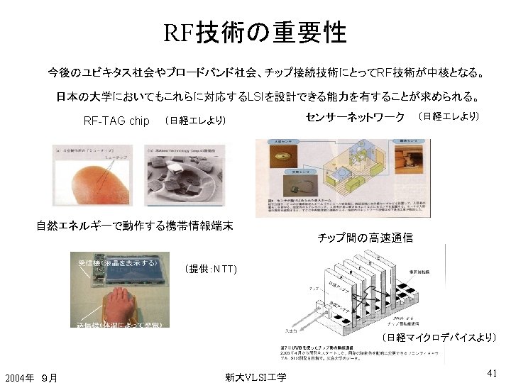
Recent developed mixed signal CMOS LSIs 5 G RF LAN 12 b 50 MHz ADC 2 ch 12 b 50 MHz DAC 2 ch Digital network 1394 b (1 GHz) AFE (Analog Front End) AFE for Digital Camera 12 b 20 MHz ADC+AGC AFE for ADLS 12 b 20 MHz ADC+DAC 2 GHz RF CMOS 2004年 9月 新大VLSI 学 15

CMOS technology for over GHz networking Digital consumer needs over GHz wire line networking. CMOS has attained 5 Gbps data transfer. World first 1394 b transceiver For 1 Gbps networking 0. 25 um 3 AL_CMOS Test chip for 5 Gbps wire line 0. 18 um 4 AL_CMOS 5 Gbps Eye pattern 2004年 9月 新大VLSI 学 16

Application area in mixed signal CMOS tech. Almost all the products need mixed signal CMOS LSI tech. ・Cellular phone: PDC, W-CDMA Wireless ・RR-Net: Bluetooth, IEEE 802. 11 ・Broad cast: STB, DTV, DAB Network Communication ・Optical: FTTH, OC-xx Wired Recording ・Metal: ADSL, VDSL, Power line modem ・Serial: IEEE 1394, USB, Ethernet ・Parallel: DVI, LVDS ・DVD, VDC, HDD Output Input Power supply 2004年 9月 ・LCD, PDP, EL, Audio drive ・Camera, Others ・ Switching supply, Every LSIs (On-chip) 新大VLSI 学 17

Difficulty of analog in LSI technology Dynamic range has been reduced with technology scaling. Performance (Log) New circuit technology or architecture are needed L Integration tox Leff Speed Dynamic range = W Xj 0. 7 x Scaling Rule Signal swing Noise + mismatch Scaling (Log) 2004年 9月 新大VLSI 学 19

CMOS as analog device CMOS has many issues as analog device, but also has a variety of circuit techniques CMOS Bipolar Comment Switch action ++ -- Low Input current ++ -- Only CMOS can realize switched capacitor circuits High gm - + CMOS is ¼ of Bip. Low Capacitance + - This results in Cp issue f. T + + Almost same Voltage mismatch -- ++ CMOS is 10 x of Bip. 1/f noise -- ++ CMOS is 10 x to 100 x of Bip. Low Sub. effect - + Offset cancel ++ -- Analog calibration ++ -- Digital calibration ++ -- Embed in CMOS ++ -- 2004年 9月 新大VLSI 学 CMOS has a variety of techniques to address the self issues 20

GHz operation by CMOS Cutoff frequency of MOS becomes higher than that of Bipolar. Over several GHz operations have attained in CMOS technology 0. 13 um 100 G 0. 18 um 0. 25 um Frequency (Hz) 50 G 20 G f. T : Bipolar (w/o Si. Ge) f. T /10 (CMOS ) 0. 35 um RF circuits 10 G 5 G f. T : CMOS Cellular Phone CDMA 5 GHz W-LAN f. T /60 (CMOS ) Digital circuits 2 G 1 G IEEE 1394 D R/C for HDD 500 M 200 M 1995 2004年 9月 2005 2000 新大VLSI 学 Year 21

Transistor issue: VT mismatch Larger gate area is needed for small VT mismatch. Scaling and proper channel structure can improve this issue. ΔVT (σ: m. V) 0. 4 um Nch Tox scaling Larger gate area 0. 13 um Nch Boron w. Halo* 0. 4 um Pch Channel engineering 0. 13 um Nch In w/o Halo* * Morifuji, et al. , IEDM 2000. 2004年 9月 新大VLSI 学 22
 Gm is proportional to Ids and inversely proportional to Veff")
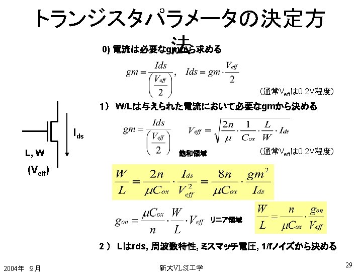
Characteristics of gm (Basic) Gm is proportional to Ids and inversely proportional to Veff is proportional to square root of Ids and inversely proportional to square root of (W/L) ratio. Square law region 2004年 9月 新大VLSI 学 25
 gds can be reduced by using larger L and small Ids. Nch")
gds (=/rds) gds can be reduced by using larger L and small Ids. Nch log [gds ] gds ∝Ids 0. 5 J L=0. 4 um J H -4 JJJ JJ J H J J J HHHH J H H H gds ∝Ids 0. 75 log [gds ] -4 -5 H H -6 B -5 B L=0. 4 um -6 0. 6 um J H 1. 0 um -7 2. 0 um 4. 0 um -6 Pch W=10 um -5 J gds ∝Ids 1. 0 um -7 2. 0 um 4. 0 um -4 -3 -2 -6 log [Ids] 2004年 9月 BBB BB J B BJ J B J B J J 0. 6 um gds ∝Ids 0. 75 J W=10 um -5 -4 -3 log [Ids] 新大VLSI 学 26
 Pr DVD Digital")
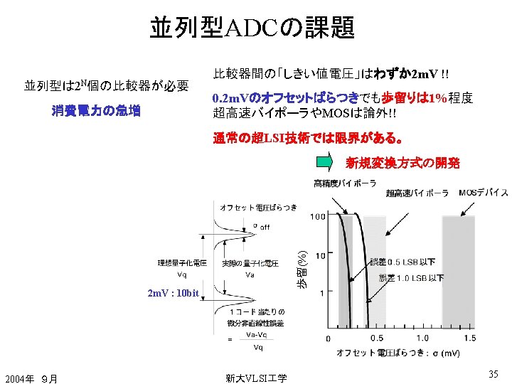
ADCの性能・用途・変換方式 ・高速かつ高精度は難しい ・変換方式はFlash, Pipeline, ΣΔ型に絞られる 1000 Flash HDD Conversion Frequency (MHz) Pr DVD Digital I/F 100 og re ss Digital TV Digital Camera VDSL 10 Pipeline 1 of te ch no lo gy ADSL Motor servo GSM handset DVD Audio Sigma Delta 0. 1 DVD Player Cellular phone Conventional Audio 0. 01 0 2 4 6 8 10 12 14 16 18 CD/MD 20 22 24 Resolution(bit) 2004年 9月 新大VLSI 学 31

ADC Architecture: Flash and pipeline Flash is used in ultra-high speed conversion with low resolution. Pipeline is used in high resolution with moderate conversion speed. Flash Deliverables; Folding Interpolation + + + + vin D 2 D 3 D 4 D 5 D 6 D 7 1 -bit DAP 1 -bit DAP S/H 2004年 9月 Digital approximater (DAP) + × 2 Amplifier Suitable for CMOS Switched capacitor operation Comparator Ultra-high speed (-- 2 GHz) Low resolution (<8 bit) Large power consumption LSB D 1 Comparator Encoder Vref Vin CLK Pipeline MSB High resolution(<14 bit) Moderate speed(<100 MHz) Low power consumption 新大VLSI 学 32

ADC Architecture: Sigma delta ADC and DAC are widely used for high resolution (14 b-24 b) and not high speed ( <1 MHz) applications. All are realized with CMOS tech. Sigma delta ADC Sigma delta DAC Integrator x(n) AVDD Comparator + z-1 + + 1 bit DAC Analog Digital Signal Processing High SNR and resolution Φ 1 C Φ 2 Digital Filter C Integrator vin DAC out Φ 1 M: over sampling ratio + Small and simple low accuracy analog ckt. 1 bit DAC 2004年 9月 Easy implementation in CMOS 新大VLSI 学 33

Progress in A/D converter ADC is a key for mixed signal technology. We have reduced the cost and power of ADC drastically; Power consumption: 1/2, 000 Price: 1/200, 000 1982 1993 Now Conventional product World 1 st Monolithic World lowest power So. C Core Board Level (Disc. +Bip) 20 W $ 8, 000 Bipolar (3 um) 2 W $ 800 Analog Devices Inc. Our developed. 2004年 9月 新大VLSI 学 CMOS (1. 2 um) CMOS (0. 15 um) 10 m. W 30 m. W $0. 04 $ 2. 00 Our developed. 34

Early stage mixed signal CMOS LSI for CE Success of CMOS ADC and DAC enabled low cost mixed signal CMOS LSI. This also enabled low cost and low power digital portable AV products. 1993 Model: Portable VCR with digital image stabilizing 6 b Video ADC Digital Video filter System block diagram 8 b low speed ADC; DAC 2004年 9月 8 b CPU 新大VLSI 学 37

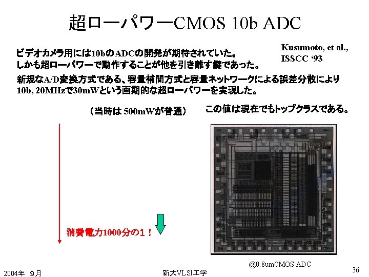
Progress in high-speed ADC High speed ADC has reduced its power and area down to be embedded. World fastest 6 b ADC 6 b, 1 GHz ADC 2 W, 1. 5 um Bipolar ISSCC 1991 6 b, 800 MHz ADC 400 m. W, 2 mm 2 0. 25 um. CMOS Pd/2 N[m. W] ISSCC 2000 World fastest CMOS ADC 10 Reported Pd of CMOS ADCs 2004年 9月 新大VLSI 学 s / 1 W 0 m 1 ISSCC 2002 World lowest Pd HS ADC 7 b, 400 MHz ADC 50 m. W, 0. 3 mm 2 0. 18 um. CMOS p Gs 0. 1 1 m 1 s sp G W/ 1 order down This Work 10 Conversion rate [x 100 Msps] 38

RF CMOS技術 2004年 9月 新大VLSI 学 39

Technology edge RF CMOS LSI Many RF CMOS LSIs have been developed for many standards Wireless LAN, 802. 11 a/b/g 0. 25 um, 2. 5 V, 23 mm 2, 5 GHz Discrete-time Bluetooth 0. 13 um, 1. 5 V, 2. 4 GHz M. Zargari (Atheros), et al. , ISSCC 2004, pp. 96 2004年 9月 新大VLSI 学 K. Muhammad (TI), et al. , ISSCC 2004, pp. 268 42

Multi-standard issue Reconfigurable RF circuit is strongly needed for solving multi-standard issue. Multi-standards and multi chips Future cellular phone needs 11 wireless standard!! IMT-2000 RF IMT-2000 BB GSM RF GSM BB Bluetooth RF Bluetooth BB MCU GPS RF GPS BB Power Unification Reconfigurable RF Yrjo Neuvo, ISSCC 2004, pp. 32 Current Future DSP Unified wireless system 2004年 9月 新大VLSI 学 43

RF MEMS switch Mechanical low-loss integrated switch enables; Select or change inductance and capacitance Select signals and circuits; As a result, enables reconfigurable RF circuits J. De. Natale, ISSCC 2004, pp. 310 2004年 9月 新大VLSI 学 45

Full DVD system integration in 0. 13 um tech. Advanced mixed signal So. C has been successfully developed. Okamoto, et al. , ISSCC 2003 0. 13 um, Cu 6 Layer, 24 MTr CPU 2 CPU1 System Controller Pixel Operation Processor Front-End Analog FE +Digital R/C VCO ADC PRML Read Channel AV Decode Processor IO Processor Servo DSP Gm-C Filter Back -End Analog Front End 2004年 9月 新大VLSI 学 47

Noise and EMI reduction To reduce the noise generated by digital; Increase embedded decoupling capacities in digital and analog and also increase substrate resistance, decrease package inductances. Noise radiation Digital ckt. Noise current is converted to noise voltage Analog ckt. L RC Low-pass filter R Package inductance 2004年 9月 C R and C forms RC low pass filter Embedded decoupling capacitance Substrate resistance 新大VLSI 学 Noise invasion 51

Noise simulation Noise should be simulated on the post-layout simulation stage Without added dec-cap. With added dec-cap. Peak current can be reduced to 65% 2004年 9月 新大VLSI 学 52

ADSL Analog Front End G. C. 12 Rx Data ADC 0~- 15 d. B External Signal Process or Tx Data Digital Interface Line Digital Tuning Interface 1.1MHz 138KHz LNA 12 DAC 0 ~ 31 d. B 8 VCO DAC 2004年 9月 XTAL 新大VLSI 学 局側 : Solid lines 宅側 : Dotted lines 56

LSI design using behavioral language Example: Analog Front End chip for ADSL system. LNA Output driver Buffer Filter D/A A/D VCXO cont. Control logic 2004年 9月 新大VLSI 学 57

Hierarchical and behavioral system design System should be described in behavioral language, hierarchically. Analog: Verilog-A Logic: Verilog-D Analog behavioral model 2004年 9月 新大VLSI 学 58

Virtual System test using Verilog AMS and Matlab We can test the designed mixed signal system virtually, by using Verilog AMS and Matlab DMT modulation Conste llation ENC IFFT DMT demodulation FIR Target LSI FIR FFT Verilog-AMS Conste llation DEC Matlab is used as a soft DSP > 66 d. B Q I f MTPR TEST (DMT Carrier hole) 2004年 9月 新大VLSI 学 QAM constellation 59

Vdd and CMOS scaling limits in analog Lowest analog operating voltage must be 1. 2 V -1. 8 V. Technology node (0. 1 um) Supply voltage (V) 最新のロードマップでは 65 nmノードの動作電圧は 1. 2 V程度になっており アナログもこの程度の電圧は使用可能と思われる。 4 Analog (Upper) アナログ(上限) 3 Analog (Lower) アナログ(下限) 2 1 Digital (Lower) デジタル(下限) 0 1 2004年 9月 ITRS ‘ 99 Digital (Upper)Technology node デジタル(上限) テクノロジーノード 2 ‘ 00 3 4 5 6 7 ‘ 05 8 新大VLSI 学 9 10 11 12 ‘ 10 13 14 15 61

Cost up issue by analog & I/O Cost of mixed A/D LSI will increase when using deep sub-micron device, due to the increase of cost of non-scalable analog and I/O parts. Large analog on So. C must be unacceptable in near future. I/O Analog Wafer cost increases 1. 3 x for one generation (0. 35 um : 1) Digital Chip area 2004年 9月 Chip cost 新大VLSI 学 63

Example: Analog+ digital calibration tech. Area and power are reduced drastically, by scaled CMOS and digital tech. Y. Cong and R. L. Geiger, Iowa state university, ISSCC 2003 14 b 100 MS/s DAC 1. 5 V, 17 m. W, 0. 1 mm 2, 0. 13 um 0. 5 LSB INL, SFDR=82 d. B at 0. 9 MHz, 62 d. B at 42. 5 MHz +/- 9 LSB +/- 0. 4 LSB Area: 1/50 Pd: 1/20 Calibration 2004年 9月 新大VLSI 学 64
. Next step")
Future step: Mixed signal egg. Analog helps digital (digital network and storage…). Next step is digital must help analog. Mixed signal egg ( Analog yolk and white with digital shell) Digital shell Sustain the analog egg. Calibration and adjustment. Analog yolk and white Ultra-low power signal processing Ultra-high speed signal processing But, very delicate and fancy 2004年 9月 新大VLSI 学 65
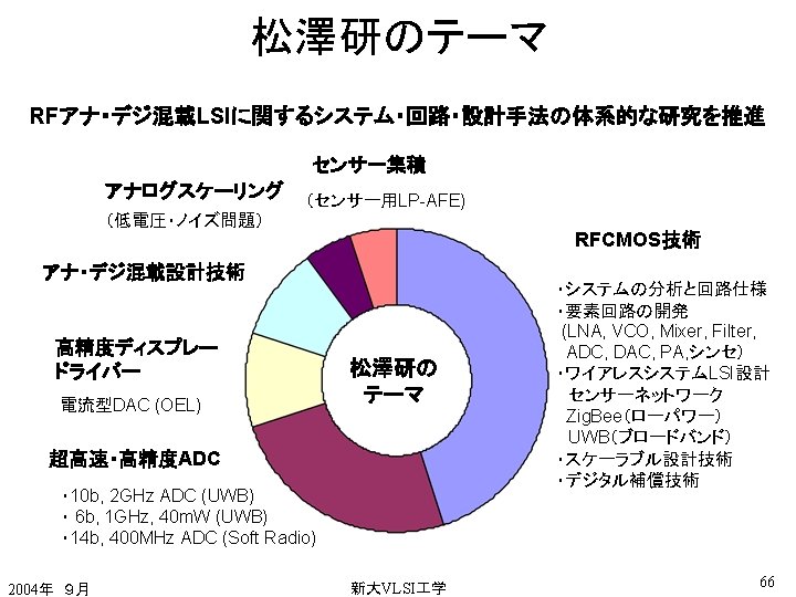
- Slides: 67