RF and ECR ion source development activities at
- Slides: 28

RF and ECR ion source development activities at VECC Ranjini Menon Variable Energy Cyclotron Centre 3/11/2021 UFCYC 2012 1

Plan of the talk • ECR ion source -6. 4 GHz - Provides low energy beam for material science experiments • ECR ion source - 14. 4 GHz - Dedicated to K-500 Cyclotron • SC ECR ion source - 18 GHz - 12 th Plan project • ICP ion source - 13. 56 MHz - Plasma Focused ion beam system 3/11/2021 UFCYC 2012 2

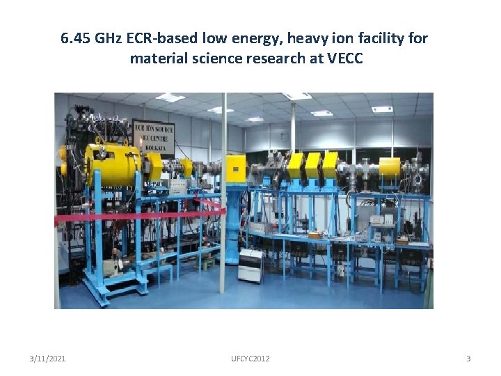
6. 45 GHz ECR-based low energy, heavy ion facility for material science research at VECC 3/11/2021 UFCYC 2012 3

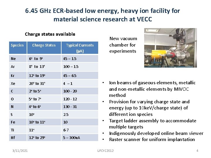
6. 45 GHz ECR-based low energy, heavy ion facility for material science research at VECC Charge states available Species Charge States Typical Currents (m. A) Ne 6+ to 9+ 45 – 1. 5 Ar 8+ to 13+ 100 – 1. 5 Kr 12+ to 19+ 45 – 6. 5 Xe 20+ to 31+ 4 – 1 C 2+ to 5+ 100 - 20 O 5+ to 7+ 120 - 12 N 4+ to 6+ 130 - 31 S 10+ 2. 5 Fe 10+ to 11+ 10 Ti 11+ 6 -7 Hf 12+ to 29+ 5 – 300 n. A 3/11/2021 New vacuum chamber for experiments • Ion beams of gaseous elements, metallic and non-metallic elements by MIVOC method • Provision for varying charge state and energy (up to 10 ke. V/charge state) of different ion species • Target ladder assembly to accommodate multiple targets • Indigenously developed online beam viewer • Raster scanner for uniform implantation UFCYC 2012 4

Experiments with the ECR ion source based low energy ion beam facility at VECC • O an N ion implantation in PMMA to study the charge state and ion species effect. (IIT Roorkee, UGCDAE-CSR & VECC) • Effect of Ar beam irradiation on the structural and physical properties of various tungstate/molybdate based thin films (Jadavpur Univ. Department of physics & VECC) • Recoil implantation of Cd. S nanoparticles in PMMA for the synthesis of templates to grow nanoparticles (IIT Roorkee, UGC-DAE-CSR & VECC ) • implantation in Ni-doped Bi. Fe. O 3 to modify ferroelectric properties (IIT Roorkee, UGC-DAE-CSR & VECC) • N implantation in Zn. O for the synthesis of p-n junction (BIT, Mesra, UGC-DAE-CSR & VECC) • N ion implantation in WO 3 to develop gas sensor properties (BIT, Mesra, UGC-DAE-CSR & VECC) • N implantation in polyaniline thin films to modify electrical and optical properties (BESU, Shibpur, UGC-DAE-CSR & VECC) • N implantation in Polyaniline thick films to study optical and electrical bulk properties. (BESU, Shibpur, UGC-DAE-CSR & VECC) • Ar implantation in reactor structural material T 91 to study the micro-structural changes. (Physical Metallurgy Section, MSD, BARC, UGC-DAE CSR, Kolkata and VECC) • Ar implantation in Thermal reactor material (Zr-1 Nb alloy) to study the change in bulk properties. 3/11/2021 UFCYC 2012 5 (Physical Metallurgy Section, MSD, BARC, UGC-DAE CSR, Kolkata & VECC)

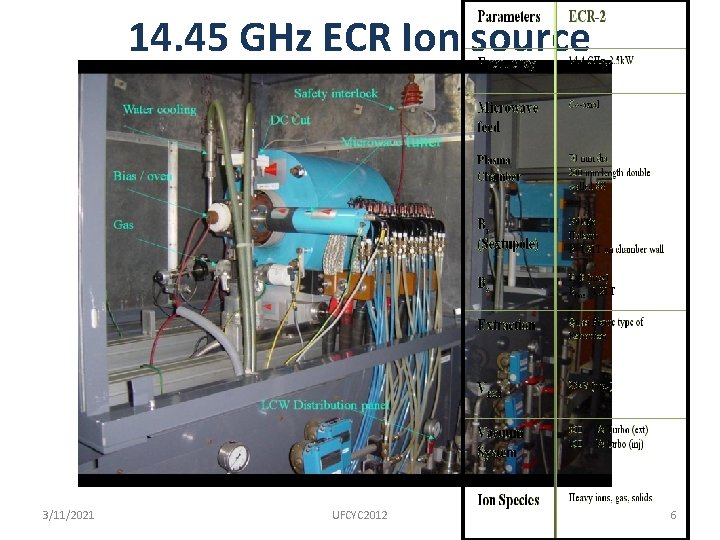
14. 45 GHz ECR Ion source 3/11/2021 UFCYC 2012 6

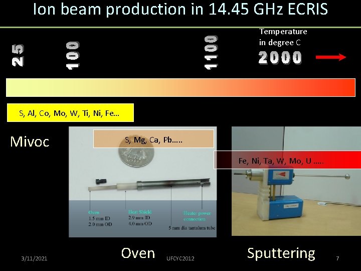
Ion beam production in 14. 45 GHz ECRIS Temperature in degree C S, Al, Co, Mo, W, Ti, Ni, Fe… Mivoc S, Mg, Ca, Pb…. . Fe, Ni, Ta, W, Mo, U …. . 3/11/2021 Oven UFCYC 2012 Sputtering 7

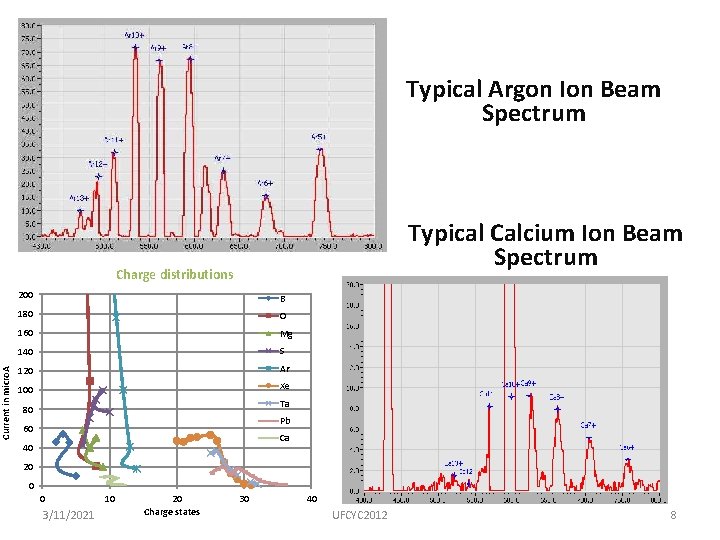
Current in micro. A Typical Argon Ion Beam Spectrum Typical Calcium Ion Beam Spectrum Charge distributions 200 B 180 O 160 Mg 140 S 120 Ar 100 Xe Ta 80 Pb 60 Ca 40 20 0 0 3/11/2021 10 20 Charge states 30 40 UFCYC 2012 8

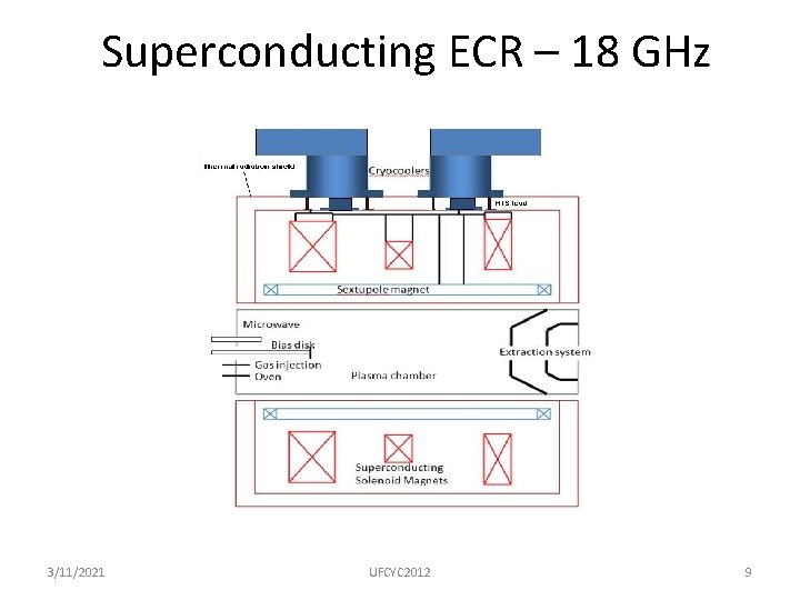
Superconducting ECR – 18 GHz 3/11/2021 UFCYC 2012 9

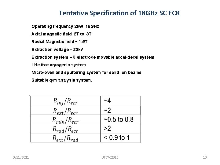
Tentative Specification of 18 GHz SC ECR Operating frequency 2 k. W, 18 GHz Axial magnetic field 2 T to 3 T Radial Magnetic field ~ 1. 5 T Extraction voltage – 20 k. V Extraction system – 3 electrode movable accel-decel system LHe free cryogenic system Micro-oven and sputtering system for solid ion beams Suitable q/m analysis system. 3/11/2021 UFCYC 2012 10

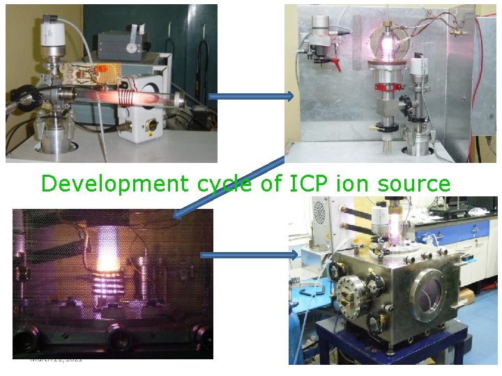
Development cycle of ICP ion source March 11, 2021 11

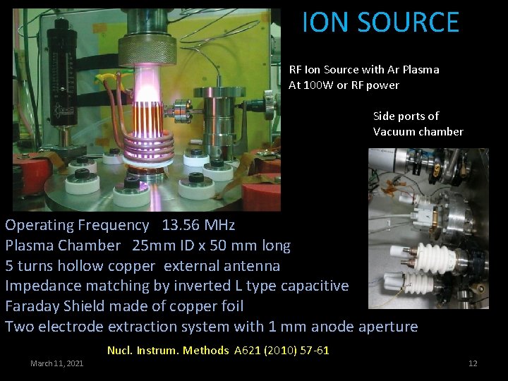
ION SOURCE RF Ion Source with Ar Plasma At 100 W or RF power Side ports of Vacuum chamber Operating Frequency 13. 56 MHz Plasma Chamber 25 mm ID x 50 mm long 5 turns hollow copper external antenna Impedance matching by inverted L type capacitive Faraday Shield made of copper foil Two electrode extraction system with 1 mm anode aperture Nucl. Instrum. Methods A 621 (2010) 57 -61 March 11, 2021 12

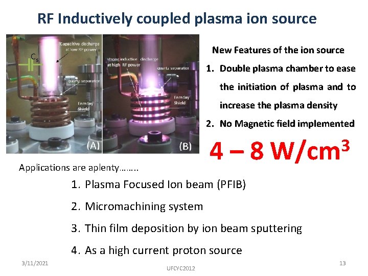
RF Inductively coupled plasma ion source New Features of the ion source Cs 1. Double plasma chamber to ease the initiation of plasma and to increase the plasma density 2. No Magnetic field implemented 4– 8 Applications are aplenty……. . 3 W/cm 1. Plasma Focused Ion beam (PFIB) 2. Micromachining system 3. Thin film deposition by ion beam sputtering 4. As a high current proton source 3/11/2021 UFCYC 2012 13

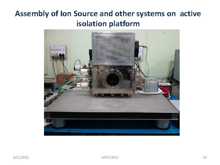
Assembly of Ion Source and other systems on active isolation platform 3/11/2021 UFCYC 2012 14

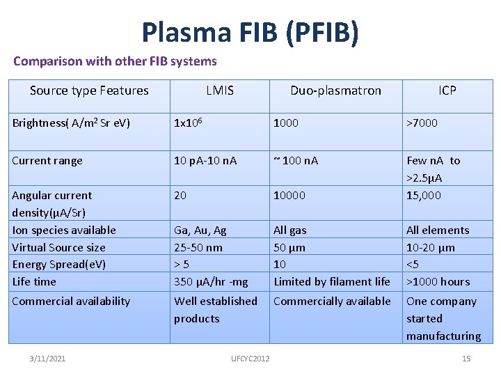
Plasma FIB (PFIB) Comparison with other FIB systems Source type Features LMIS Duo-plasmatron ICP Brightness( A/m 2 Sr e. V) 1 x 10⁶ 1000 >7000 Current range 10 p. A-10 n. A ~ 100 n. A Angular current density(µA/Sr) Ion species available Virtual Source size Energy Spread(e. V) Life time 20 10000 Few n. A to >2. 5µA 15, 000 Ga, Au, Ag 25 -50 nm > 5 350 µA/hr -mg All gas 50 µm 10 Limited by filament life All elements 10 -20 µm <5 >1000 hours Commercial availability Well established products Commercially available One company started manufacturing 3/11/2021 UFCYC 2012 15

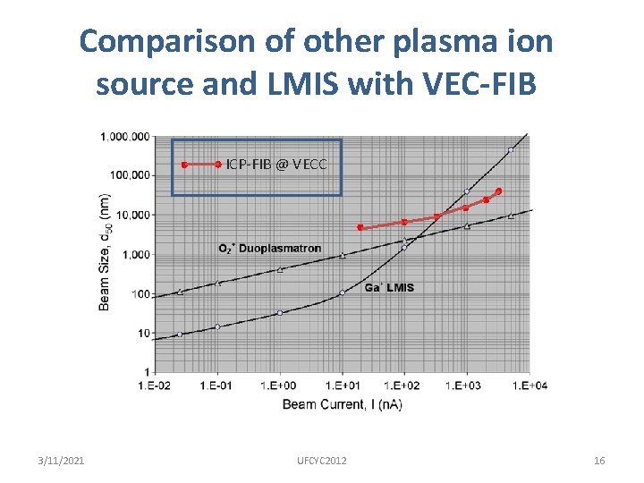
Comparison of other plasma ion source and LMIS with VEC-FIB ICP-FIB @ VECC 3/11/2021 UFCYC 2012 16

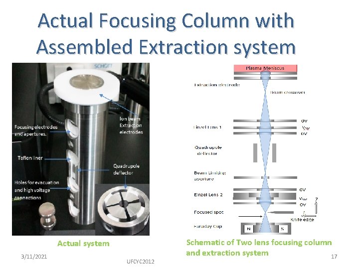
Actual Focusing Column with Assembled Extraction system Actual system 3/11/2021 UFCYC 2012 Schematic of Two lens focusing column and extraction system 17

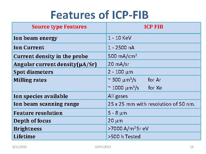
Features of ICP-FIB Source type Features ICP FIB Ion beam energy 1 - 10 Ke. V Ion Current 1 - 2500 n. A Current density in the probe Angular current density(µA/Sr) Spot diameters Milling rates Ion species available Ion beam scanning range 500 m. A/cm 2 20 m. A/sr 2 - 100 µm ~ 300 µm 3/s for Ar ~ 1000 µm 3/s for Xe All gases 25 x 25 mm with resolution of 50 nm. Feature resolution Depth of focus Brightness Lifetime 5 - 8 µm 20 µm >7000 A/m 2 Sr e. V >500 h Tested 3/11/2021 UFCYC 2012 18

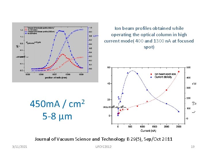
Ion beam profiles obtained while operating the optical column in high current mode( 400 and 1300 n. A at focused spot) 450 m. A / cm 2 5 -8 µm Journal of Vacuum Science and Technology B 29(5), Sep/Oct 2011 3/11/2021 UFCYC 2012 19

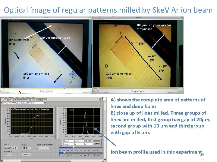
Optical image of regular patterns milled by 6 ke. V Ar ion beam 100 µm Tungsten wire for comparison Ion beam trace lines 100 µm Tungsten wire 5 µm gap A 10 µm gap B 100 µm long milled lines 20 µm gap A A) shows the complete area of patterns of lines and deep holes B) close up of lines milled. Three groups of lines are milled, first group has gap of 20µm, second group with 10 µm and third group with gap of 5 µm. March 11, 2021 Ion beam profile used in this experiment 20

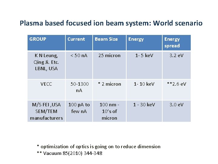
Plasma based focused ion beam system: World scenario GROUP Current Beam Size Energy spread K N Leung, Qing Ji. Etc. LBNL, USA < 50 n. A 25 micron 1 - 5 ke. V 3. 2 e. V VECC 50 -1300 n. A * 2 micron 1 - 10 ke. V **2. 6 e. V M/S FEI , USA SEM/TEM manufacturers 100 p. A to few n. A 100 nm - 10’s of micron 1 - 30 ke. V 3. 0 e. V * optimization of optics is going on to reduce dimension ** Vacuum 85(2010) 344 -348

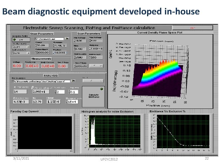
Beam diagnostic equipment developed in-house Parameter Measuring equipment Plasma density Langmuir probe Electron temperature Langmuir probe Beam intensity Faraday cup Emittance Allison scanner Brightness Allison scanner Beam width Wire scanner/ Knife edge Beam profile Wire scanner/ Knife edge Energy spread of plasma bound ions Retarding field energy analyzer (RFEA) Energy spread of extracted ion beam Variable focusing RFEA Mass Spectrometer Wien filter (Ex. B) 3/11/2021 UFCYC 2012 22

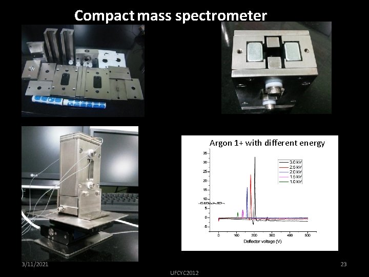
Compact mass spectrometer Argon 1+ with different energy 3/11/2021 23 UFCYC 2012

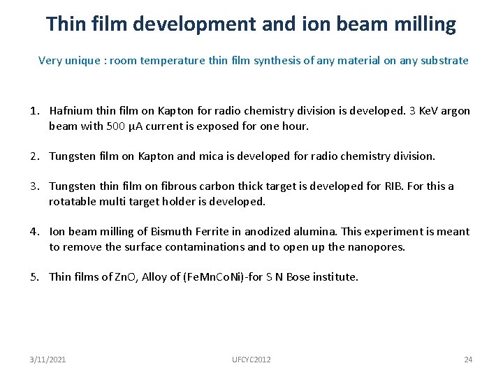
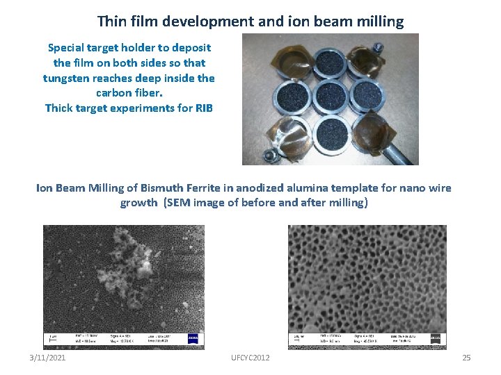
Thin film development and ion beam milling Very unique : room temperature thin film synthesis of any material on any substrate 1. Hafnium thin film on Kapton for radio chemistry division is developed. 3 Ke. V argon beam with 500 μA current is exposed for one hour. 2. Tungsten film on Kapton and mica is developed for radio chemistry division. 3. Tungsten thin film on fibrous carbon thick target is developed for RIB. For this a rotatable multi target holder is developed. 4. Ion beam milling of Bismuth Ferrite in anodized alumina. This experiment is meant to remove the surface contaminations and to open up the nanopores. 5. Thin films of Zn. O, Alloy of (Fe. Mn. Co. Ni)-for S N Bose institute. 3/11/2021 UFCYC 2012 24

Thin film development and ion beam milling Special target holder to deposit the film on both sides so that tungsten reaches deep inside the carbon fiber. Thick target experiments for RIB Simultaneous 9 targets can be coated Ion Beam Milling of Bismuth Ferrite in anodized alumina template for nano wire growth (SEM image of before and after milling) 3/11/2021 UFCYC 2012 25

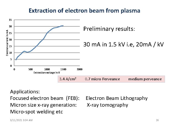
Extraction of electron beam from plasma 35 Preliminary results: Electron current in m. A 30 25 20 30 m. A in 1. 5 k. V i. e, 20 m. A / k. V 15 10 5 0 0 500 1000 1500 Extraction voltage in V 2000 3. 4 A/cm 2 0. 7 micro Perveance medium perveance Applications: Focused electron beam (FEB): Electron Beam Lithography Micron size x-ray generation: X-ray tomography Micro-spot welding etc 3/11/2021 3: 04 AM 26

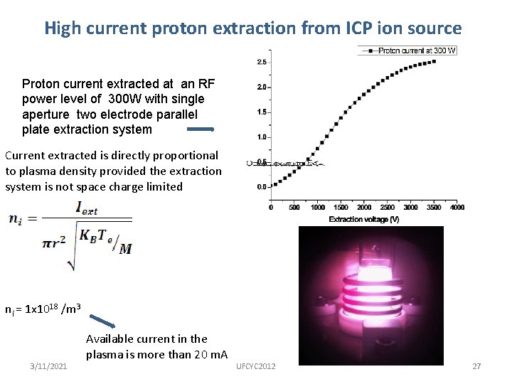
High current proton extraction from ICP ion source Proton current extracted at an RF power level of 300 W with single aperture two electrode parallel plate extraction system Current extracted is directly proportional to plasma density provided the extraction system is not space charge limited ni = 1 x 10¹⁸ /m 3 3/11/2021 Available current in the plasma is more than 20 m. A UFCYC 2012 27

• • • 3/11/2021 3: 04 AM APG MEG VECC workshop Vacuum section LCW section Electrical section Accelerator Physics team VEC ECR section SCCECR section 28