REVIEW REGISTER TRANSFER LEVEL RTL DESIGN Using ASM


- Slides: 36

REVIEW REGISTER TRANSFER LEVEL (RTL) DESIGN Using ASM CHART Chapter 8 1

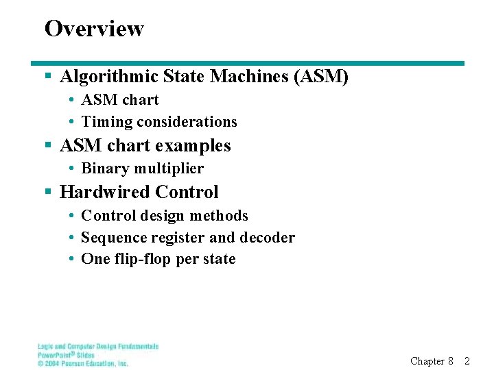
Overview § Algorithmic State Machines (ASM) • ASM chart • Timing considerations § ASM chart examples • Binary multiplier § Hardwired Control • Control design methods • Sequence register and decoder • One flip-flop per state Chapter 8 2

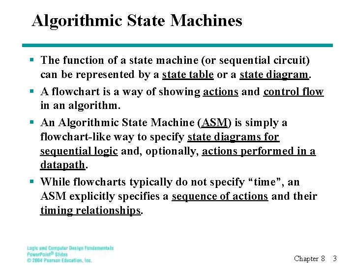
Algorithmic State Machines § The function of a state machine (or sequential circuit) can be represented by a state table or a state diagram. § A flowchart is a way of showing actions and control flow in an algorithm. § An Algorithmic State Machine (ASM) is simply a flowchart-like way to specify state diagrams for sequential logic and, optionally, actions performed in a datapath. § While flowcharts typically do not specify “time”, an ASM explicitly specifies a sequence of actions and their timing relationships. Chapter 8 3

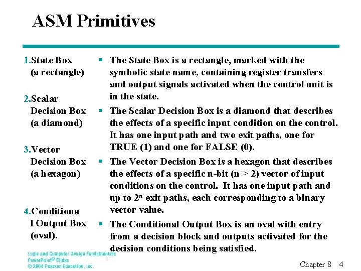
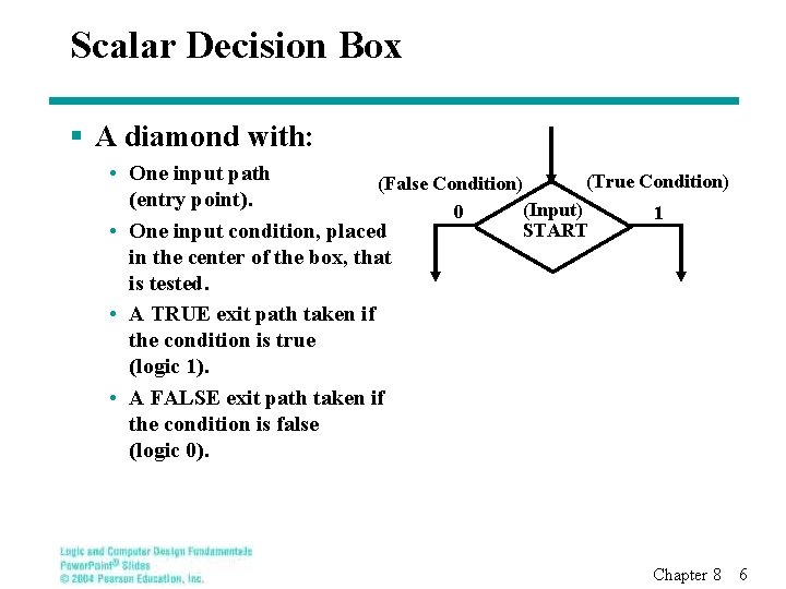
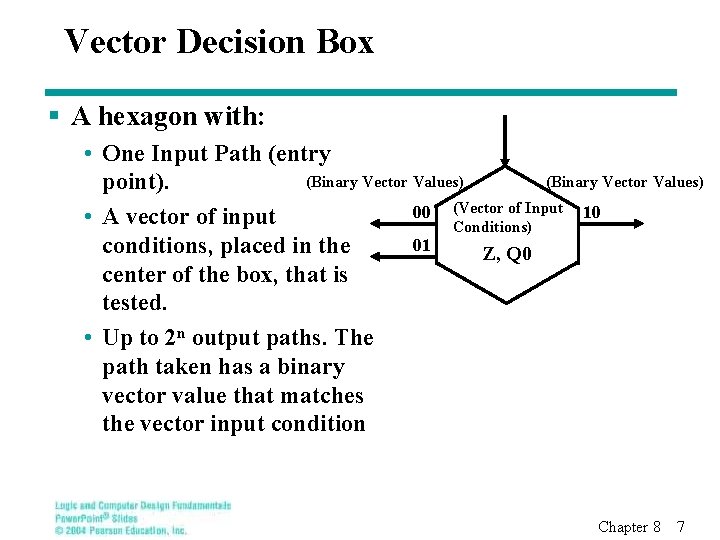
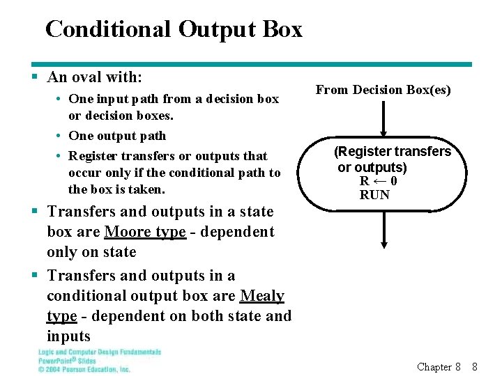
ASM Primitives 1. State Box (a rectangle) 2. Scalar Decision Box (a diamond) 3. Vector Decision Box (a hexagon) 4. Conditiona l Output Box (oval). § The State Box is a rectangle, marked with the symbolic state name, containing register transfers and output signals activated when the control unit is in the state. § The Scalar Decision Box is a diamond that describes the effects of a specific input condition on the control. It has one input path and two exit paths, one for TRUE (1) and one for FALSE (0). § The Vector Decision Box is a hexagon that describes the effects of a specific n-bit (n > 2) vector of input conditions on the control. It has one input path and up to 2 n exit paths, each corresponding to a binary vector value. § The Conditional Output Box is an oval with entry from a decision block and outputs activated for the decision conditions being satisfied. Chapter 8 4

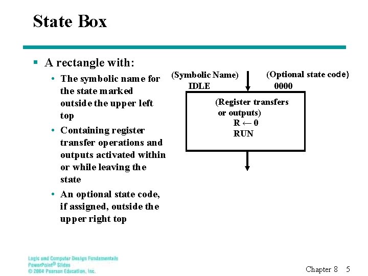
State Box § A rectangle with: (Optional state code) • The symbolic name for (Symbolic Name) IDLE 0000 the state marked (Register transfers outside the upper left or outputs) top R← 0 • Containing register RUN transfer operations and outputs activated within or while leaving the state • An optional state code, if assigned, outside the upper right top Chapter 8 5

Scalar Decision Box § A diamond with: • One input path (True Condition) (False Condition) (entry point). (Input) 0 1 START • One input condition, placed in the center of the box, that is tested. • A TRUE exit path taken if the condition is true (logic 1). • A FALSE exit path taken if the condition is false (logic 0). Chapter 8 6

Vector Decision Box § A hexagon with: • One Input Path (entry (Binary Vector Values) point). 00 (Vector of Input 10 • A vector of input Conditions) 01 conditions, placed in the Z, Q 0 center of the box, that is tested. • Up to 2 n output paths. The path taken has a binary vector value that matches the vector input condition Chapter 8 7

Conditional Output Box § An oval with: • One input path from a decision box or decision boxes. • One output path • Register transfers or outputs that occur only if the conditional path to the box is taken. § Transfers and outputs in a state box are Moore type - dependent only on state § Transfers and outputs in a conditional output box are Mealy type - dependent on both state and inputs From Decision Box(es) (Register transfers or outputs) R← 0 RUN Chapter 8 8

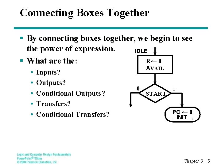
Connecting Boxes Together § By connecting boxes together, we begin to see the power of expression. IDLE R← 0 § What are the: • • • Inputs? Outputs? Conditional Outputs? Transfers? Conditional Transfers? AVAIL 0 START 1 PC ← 0 INIT Chapter 8 9

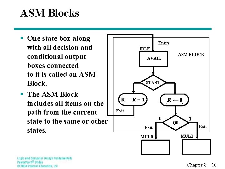
ASM Blocks § One state box along with all decision and conditional output boxes connected to it is called an ASM Block. § The ASM Block includes all items on the path from the current state to the same or other states. Entry IDLE AVAIL ASM BLOCK START R← R + 1 R← 0 Exit MUL 0 Q 0 1 Exit MUL 1 Chapter 8 10

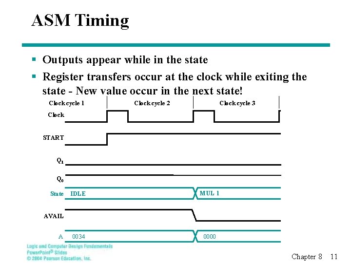
ASM Timing § Outputs appear while in the state § Register transfers occur at the clock while exiting the state - New value occur in the next state! Clock cycle 1 Clock cycle 2 Clock cycle 3 Clock START Q 1 Q 0 State IDLE MUL 1 0034 0000 AVAIL A Chapter 8 11

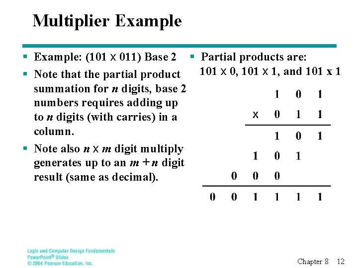
Multiplier Example § Example: (101 x 011) Base 2 § Partial products are: 101 x 0, 101 x 1, and 101 x 1 § Note that the partial product summation for n digits, base 2 numbers requires adding up to n digits (with carries) in a column. § Note also n x m digit multiply generates up to an m + n digit result (same as decimal). Chapter 8 12

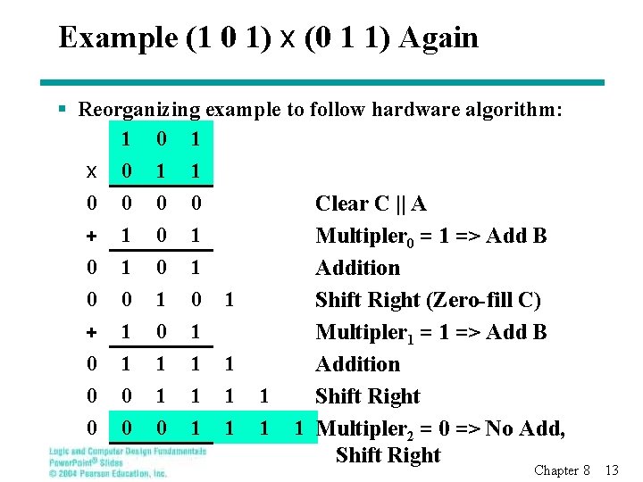
Example (1 0 1) x (0 1 1) Again § Reorganizing example to follow hardware algorithm: 1 0 1 x 0 1 1 0 + 0 0 0 0 1 1 0 0 0 1 0 1 1 1 Clear C || A Multipler 0 = 1 => Add B Addition Shift Right (Zero-fill C) Multipler 1 => Add B Addition Shift Right 1 Multipler 2 = 0 => No Add, Shift Right Chapter 8 13

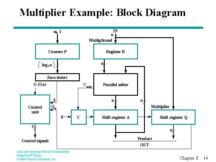
Multiplier Example: Block Diagram IN n Multiplicand n 2 1 Counter P Register B n log 2 n Zero detect G (Go) Control unit C Z Qo out Parallel adder n n Multiplier 0 C Shift register A Shift register Q 4 Control signals n Product OUT Chapter 8 14

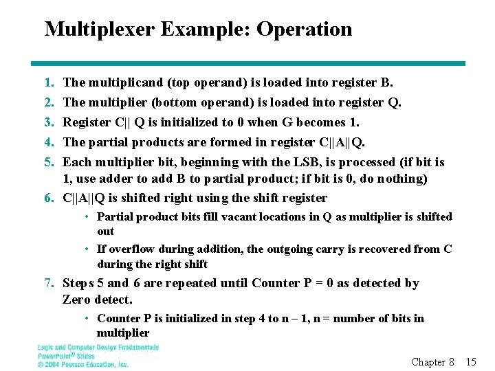
Multiplexer Example: Operation 1. 2. 3. 4. 5. The multiplicand (top operand) is loaded into register B. The multiplier (bottom operand) is loaded into register Q. Register C|| Q is initialized to 0 when G becomes 1. The partial products are formed in register C||A||Q. Each multiplier bit, beginning with the LSB, is processed (if bit is 1, use adder to add B to partial product; if bit is 0, do nothing) 6. C||A||Q is shifted right using the shift register • Partial product bits fill vacant locations in Q as multiplier is shifted out • If overflow during addition, the outgoing carry is recovered from C during the right shift 7. Steps 5 and 6 are repeated until Counter P = 0 as detected by Zero detect. • Counter P is initialized in step 4 to n – 1, n = number of bits in multiplier Chapter 8 15

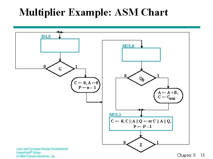
Multiplier Example: ASM Chart IDLE MUL 0 0 G 1 0 C ← 0, A ← 0 P ←n – 1 Q 0 1 A ← A + B, C ← Cout MUL 1 C ← 0, C || A || Q ← sr C || A || Q, P ← P – 1 0 Z 1 Chapter 8 16

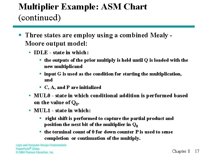
Multiplier Example: ASM Chart (continued) § Three states are employ using a combined Mealy Moore output model: • IDLE - state in which: § the outputs of the prior multiply is held until Q is loaded with the new multiplicand § input G is used as the condition for starting the multiplication, and § C, A, and P are initialized • MUL 0 - state in which conditional addition is performed based on the value of Q 0. • MUL 1 - state in which: § right shift is performed to capture the partial product and position the next bit of the multiplier in Q 0 § the terminal count of 0 for down counter P is used to sense completion or continuation of the multiply. Chapter 8 17

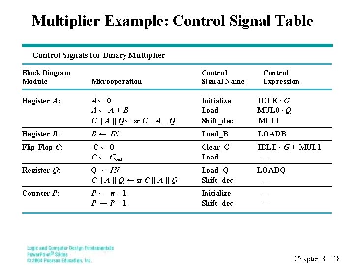
Multiplier Example: Control Signal Table Control Signals for Binary Multiplier Block Diagram Module Microope ration Control Si gn al N ame Contro l Expression Register A: A← 0 A←A + B C || A || Q ← sr C || A || Q Initialize Load Shift_dec IDLE · G MUL 0 · Q MUL 1 Register B: B ← IN Load_B LOADB Flip-Flop C: C ← 0 C ← C out Clear_C Load IDLE · G + MUL 1 — Register Q: Q ← IN C || A || Q ← sr C || A || Q Load_Q Shift_dec LOADQ — Counter P: P← n– 1 P ←P– 1 Initialize Shift_dec — — Chapter 8 18

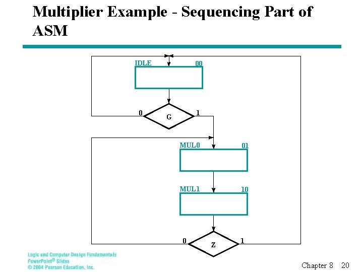
Multiplier Example: Control Table (continued) § Signals are defined on a register basis § LOADQ and LOADB are external signals controlled from the system using the multiplier and will not be considered a part of this design § Note that many of the control signals are “reused” for different registers. § These control signals are the “outputs” of the control unit § With the outputs represented by the table, they can be removed from the ASM giving an ASM that represents only the sequencing (next state) behavior Chapter 8 19

Multiplier Example - Sequencing Part of ASM IDLE 0 00 1 G MUL 0 01 MUL 1 10 0 Z 1 Chapter 8 20

Hardwired Control § Control Design Methods • The procedure from Chapter 6 • Procedure specializations that use a single signal to represent each state § Sequence Register and Decoder • Sequence register with encoded states, e. g. , 00, 01, 10, 11. • Decoder outputs produce “state” signals, e. g. , 0001, 0010, 0100, 1000. § One Flip-flop per State • Flip-flop outputs as “state” signals, e. g. , 0001, 0010, 0100, 1000. Chapter 8 21

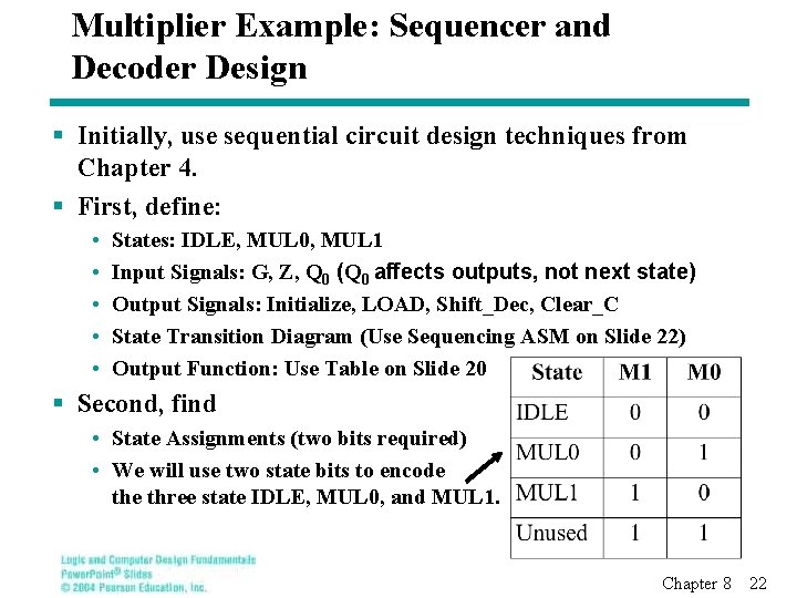
Multiplier Example: Sequencer and Decoder Design § Initially, use sequential circuit design techniques from Chapter 4. § First, define: • • • States: IDLE, MUL 0, MUL 1 Input Signals: G, Z, Q 0 (Q 0 affects outputs, not next state) Output Signals: Initialize, LOAD, Shift_Dec, Clear_C State Transition Diagram (Use Sequencing ASM on Slide 22) Output Function: Use Table on Slide 20 § Second, find • State Assignments (two bits required) • We will use two state bits to encode three state IDLE, MUL 0, and MUL 1. Chapter 8 22

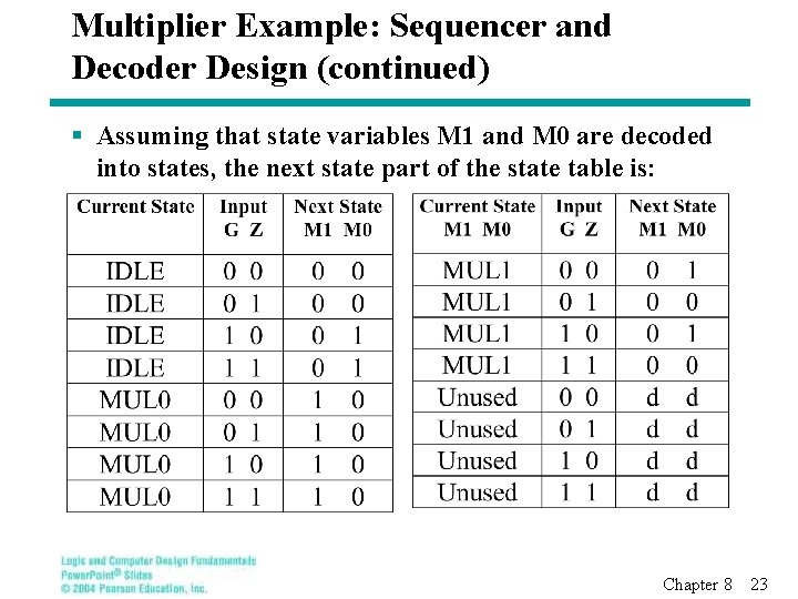
Multiplier Example: Sequencer and Decoder Design (continued) § Assuming that state variables M 1 and M 0 are decoded into states, the next state part of the state table is: Chapter 8 23

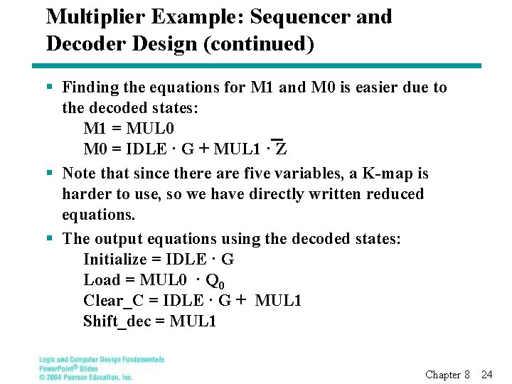
Multiplier Example: Sequencer and Decoder Design (continued) § Finding the equations for M 1 and M 0 is easier due to the decoded states: M 1 = MUL 0 M 0 = IDLE · G + MUL 1 · Z § Note that since there are five variables, a K-map is harder to use, so we have directly written reduced equations. § The output equations using the decoded states: Initialize = IDLE · G Load = MUL 0 · Q 0 Clear_C = IDLE · G + MUL 1 Shift_dec = MUL 1 Chapter 8 24

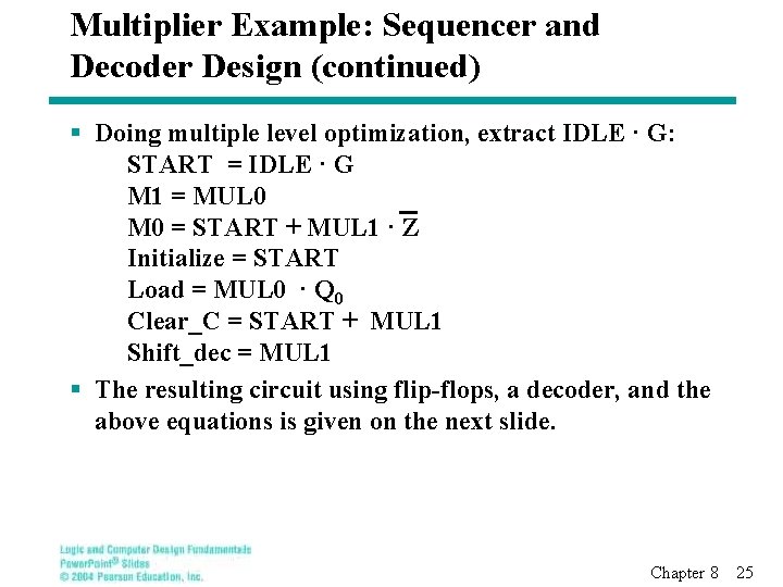
Multiplier Example: Sequencer and Decoder Design (continued) § Doing multiple level optimization, extract IDLE · G: START = IDLE · G M 1 = MUL 0 M 0 = START + MUL 1 · Z Initialize = START Load = MUL 0 · Q 0 Clear_C = START + MUL 1 Shift_dec = MUL 1 § The resulting circuit using flip-flops, a decoder, and the above equations is given on the next slide. Chapter 8 25

Multiplier Example: Sequencer and Decoder Design (continued) START G Z Initialize M 0 D C Clear_C DECODER A 0 0 1 2 A 1 3 IDLE MUL 0 MUL 1 Shift_dec M 1 D C Q 0 Load Chapter 8 26

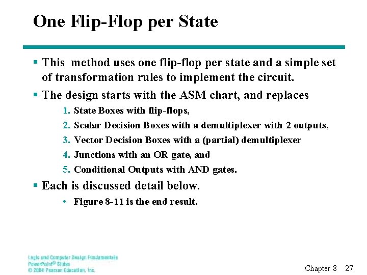
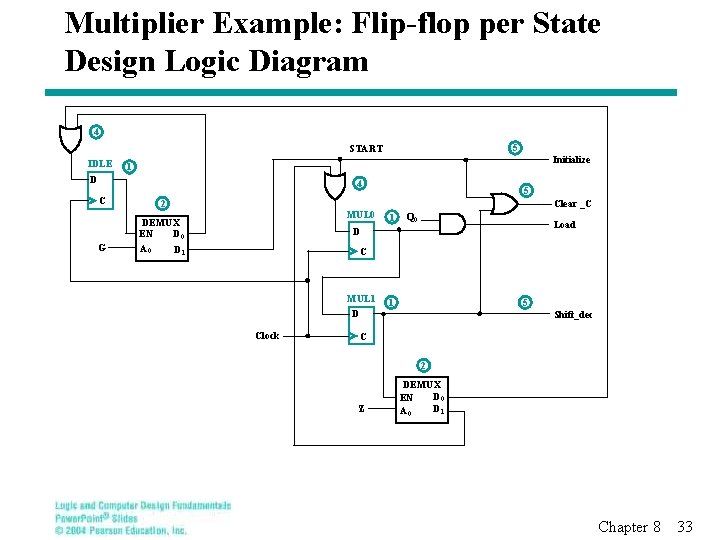
One Flip-Flop per State § This method uses one flip-flop per state and a simple set of transformation rules to implement the circuit. § The design starts with the ASM chart, and replaces 1. 2. 3. 4. 5. State Boxes with flip-flops, Scalar Decision Boxes with a demultiplexer with 2 outputs, Vector Decision Boxes with a (partial) demultiplexer Junctions with an OR gate, and Conditional Outputs with AND gates. § Each is discussed detail below. • Figure 8 -11 is the end result. Chapter 8 27

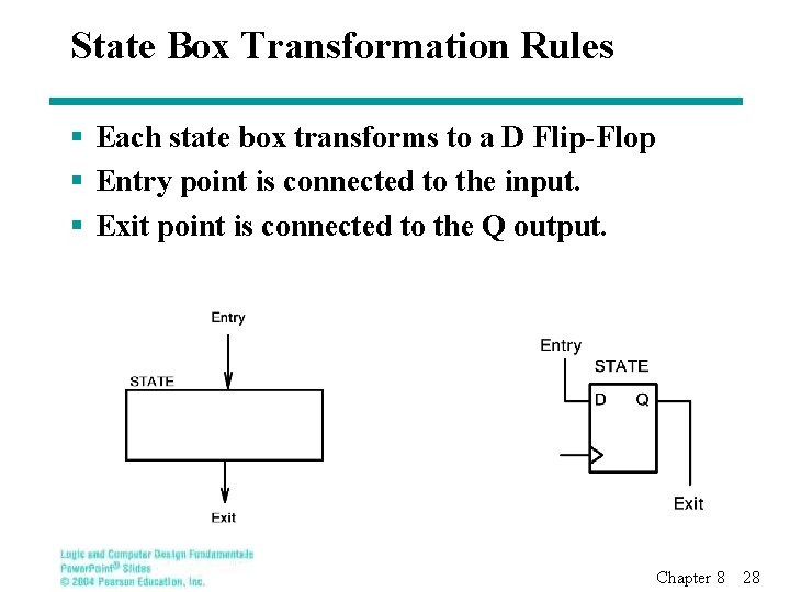
State Box Transformation Rules § Each state box transforms to a D Flip-Flop § Entry point is connected to the input. § Exit point is connected to the Q output. Chapter 8 28

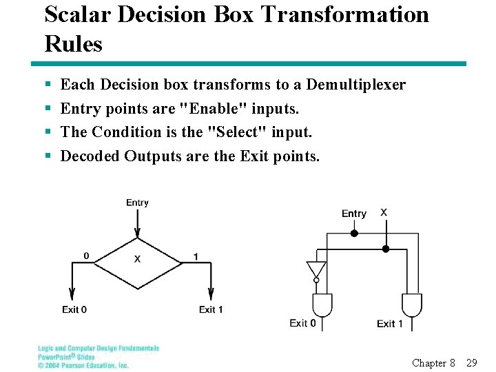
Scalar Decision Box Transformation Rules § § Each Decision box transforms to a Demultiplexer Entry points are "Enable" inputs. The Condition is the "Select" input. Decoded Outputs are the Exit points. Chapter 8 29

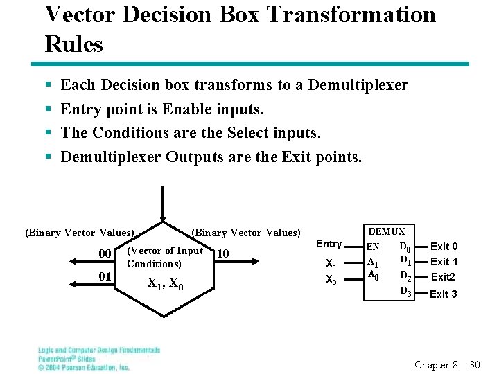
Vector Decision Box Transformation Rules § § Each Decision box transforms to a Demultiplexer Entry point is Enable inputs. The Conditions are the Select inputs. Demultiplexer Outputs are the Exit points. (Binary Vector Values) 00 01 (Binary Vector Values) (Vector of Input Conditions) X 1 , X 0 10 Entry X 1 X 0 DEMUX D 0 EN D 1 A 0 D 2 Exit 0 Exit 1 Exit 2 D 3 Exit 3 Chapter 8 30

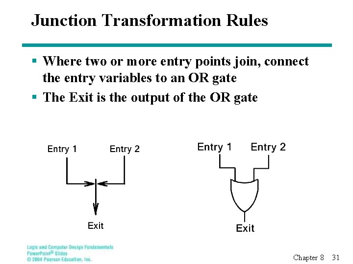
Junction Transformation Rules § Where two or more entry points join, connect the entry variables to an OR gate § The Exit is the output of the OR gate Chapter 8 31

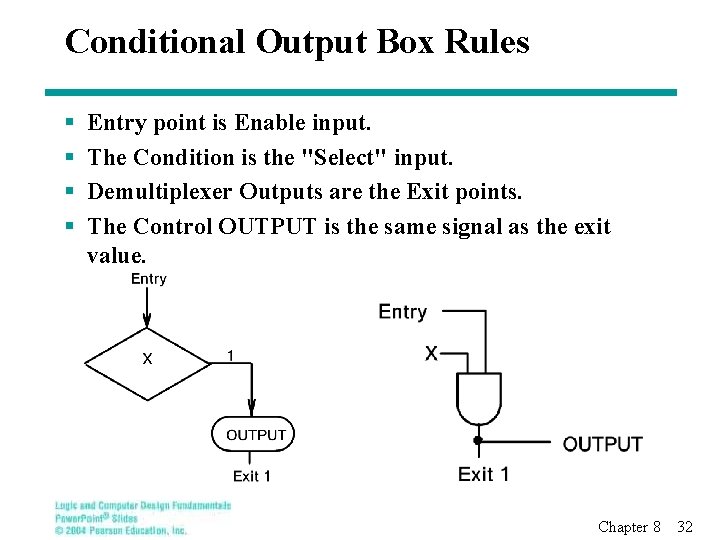
Conditional Output Box Rules § § Entry point is Enable input. The Condition is the "Select" input. Demultiplexer Outputs are the Exit points. The Control OUTPUT is the same signal as the exit value. Chapter 8 32

Multiplier Example: Flip-flop per State Design Logic Diagram 4 5 START IDLE Initialize 1 D 4 C G 2 MUL 0 DEMUX D 0 EN A 0 D 1 5 Clear _C 1 Q 0 Load D C MUL 1 D Clock 1 5 Shift_dec C 2 Z DEMUX D 0 EN D 1 A 0 Chapter 8 33

Speeding Up the Multiplier § In processing each bit of the multiplier, the circuit visits states MUL 0 and MUL 1 in sequence. § By redesigning the multiplier, is it possible to visit only a single state per bit processed? Chapter 8 34

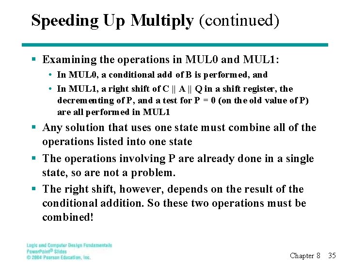
Speeding Up Multiply (continued) § Examining the operations in MUL 0 and MUL 1: • In MUL 0, a conditional add of B is performed, and • In MUL 1, a right shift of C || A || Q in a shift register, the decrementing of P, and a test for P = 0 (on the old value of P) are all performed in MUL 1 § Any solution that uses one state must combine all of the operations listed into one state § The operations involving P are already done in a single state, so are not a problem. § The right shift, however, depends on the result of the conditional addition. So these two operations must be combined! Chapter 8 35

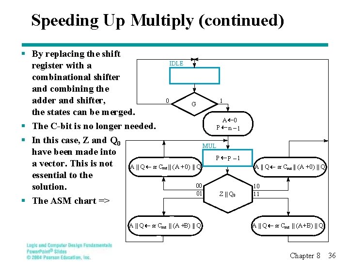
Speeding Up Multiply (continued) § By replacing the shift register with a combinational shifter and combining the adder and shifter, the states can be merged. § The C-bit is no longer needed. § In this case, Z and Q 0 have been made into a vector. This is not A || Q sr C essential to the solution. § The ASM chart => IDLE 0 out A || Q 1 G A P 0 n – 1 MUL P P– 1 || (A + 0) || Q 00 01 sr Cout || (A +B) || Q A || Q Z || Q 0 sr Cout || (A +0) || Q 10 11 A || Q sr Cout || (A+B) || Q Chapter 8 36