
Review of Vertex Detector RD for International Linear
- Slides: 36
Review of Vertex Detector R&D for International Linear Collider • ILC • Vertex Detector R&D - CCD (ISSI) - MAPS - DEPFET • Summary Jik Lee Seoul National Univ. ACFA 7 J. Lee 2020 -12 -03 1
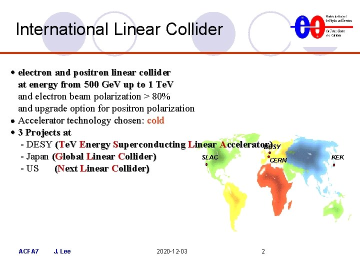
International Linear Collider · electron and positron linear collider at energy from 500 Ge. V up to 1 Te. V and electron beam polarization > 80% and upgrade option for positron polarization Accelerator technology chosen: cold · 3 Projects at - DESY (Te. V Energy Superconducting Linear Accelerator) DESY - Japan (Global Linear Collider) SLAC CERN - US (Next Linear Collider) ACFA 7 J. Lee 2020 -12 -03 2 KEK
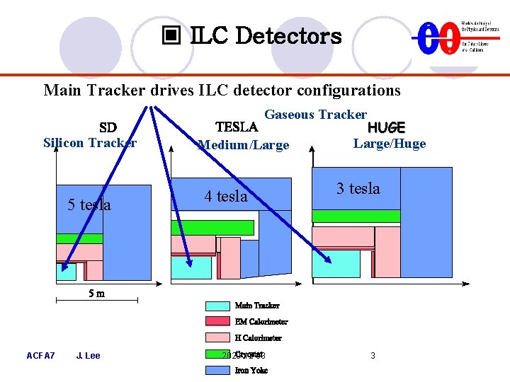
▣ ILC Detectors Main Tracker drives ILC detector configurations Silicon Tracker 5 tesla ACFA 7 J. Lee Gaseous Tracker HUGE Large/Huge Medium/Large 4 tesla 2020 -12 -03 3 tesla 3
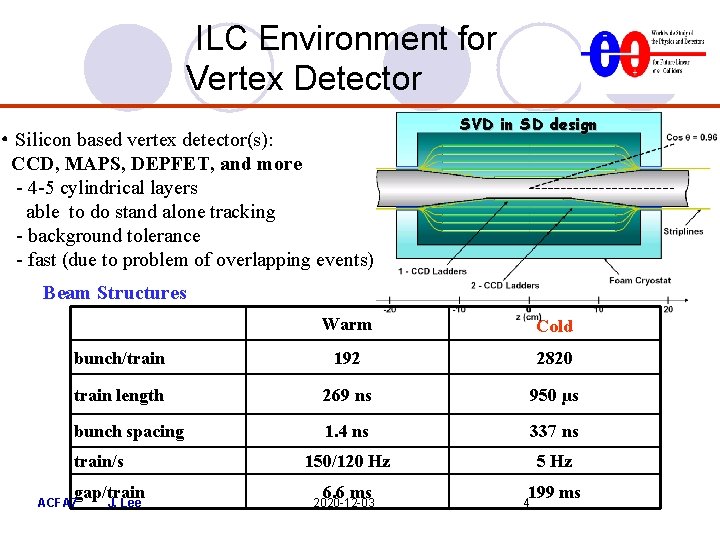
ILC Environment for Vertex Detector • Silicon based vertex detector(s): CCD, MAPS, DEPFET, and more - 4 -5 cylindrical layers able to do stand alone tracking - background tolerance - fast (due to problem of overlapping events) SVD in SD design Beam Structures Warm Cold bunch/train 192 2820 train length 269 ns 950 µs bunch spacing 1. 4 ns 337 ns 150/120 Hz 5 Hz train/s gap/train ACFA 7 J. Lee 6. 6 ms 2020 -12 -03 199 ms 4
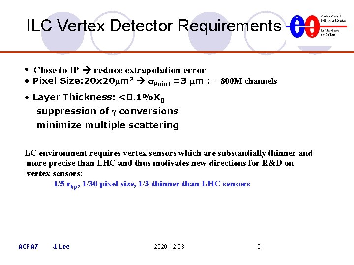
ILC Vertex Detector Requirements • Close to IP reduce extrapolation error • Pixel Size: 20 x 20 mm 2 s. Point =3 mm : ~800 M channels • Layer Thickness: <0. 1%X 0 suppression of g conversions minimize multiple scattering LC environment requires vertex sensors which are substantially thinner and more precise than LHC and thus motivates new directions for R&D on vertex sensors: 1/5 rbp, 1/30 pixel size, 1/3 thinner than LHC sensors ACFA 7 J. Lee 2020 -12 -03 5
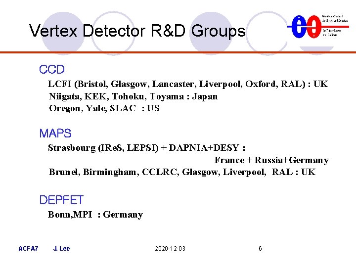
Vertex Detector R&D Groups CCD LCFI (Bristol, Glasgow, Lancaster, Liverpool, Oxford, RAL) : UK Niigata, KEK, Tohoku, Toyama : Japan Oregon, Yale, SLAC : US MAPS Strasbourg (IRe. S, LEPSI) + DAPNIA+DESY : France + Russia+Germany Brunel, Birmingham, CCLRC, Glasgow, Liverpool, RAL : UK DEPFET Bonn, MPI : Germany ACFA 7 J. Lee 2020 -12 -03 6
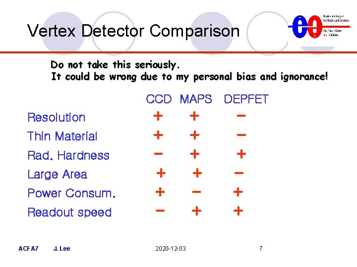
Vertex Detector Comparison Do not take this seriously. It could be wrong due to my personal bias and ignorance! CCD MAPS DEPFET Resolution Thin Material Rad. Hardness Large Area Power Consum. Readout speed ACFA 7 J. Lee + + 2020 -12 -03 + + + + 7
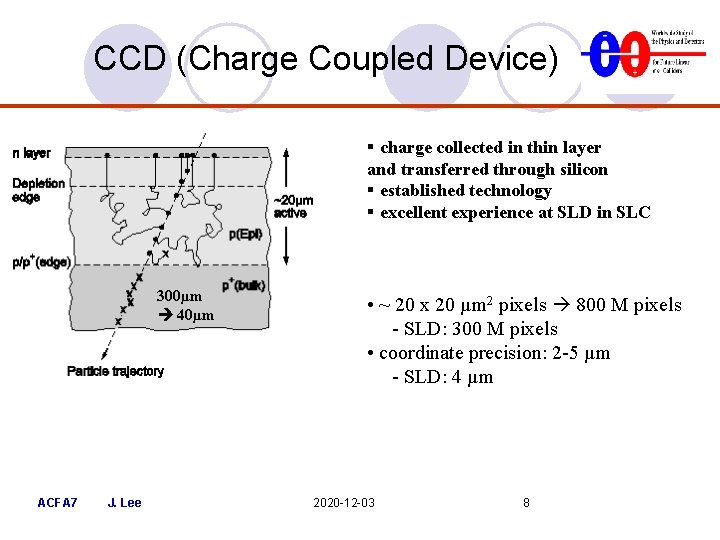
CCD (Charge Coupled Device) ▪ charge collected in thin layer and transferred through silicon ▪ established technology ▪ excellent experience at SLD in SLC 300µm 40µm ACFA 7 J. Lee • ~ 20 x 20 µm 2 pixels 800 M pixels - SLD: 300 M pixels • coordinate precision: 2 -5 µm - SLD: 4 µm 2020 -12 -03 8
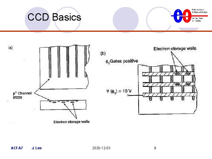
CCD Basics ACFA 7 J. Lee 2020 -12 -03 9
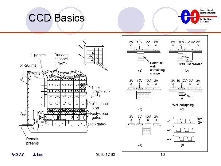
CCD Basics ACFA 7 J. Lee 2020 -12 -03 10
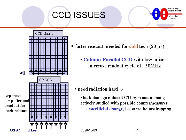
CCD ISSUES CCD classic ▪ faster readout needed for cold tech (50 µs) • Column-Parallel CCD with low noise - increase readout cycle of ~50 MHz CP CCD ▪ need radiation hard separate amplifier and readout for each column ACFA 7 J. Lee • bulk damage induced CTI by n and e- being actively studied with possible countermeasures - sacrificial charge, faster r/o before trapping 2020 -12 -03 11
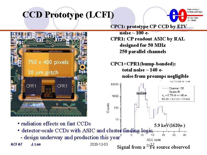
CCD Prototype (LCFI) CPC 1: prototype CP CCD by E 2 V noise ~ 100 e. CPR 1: CP readout ASIC by RAL designed for 50 MHz 250 parallel channels 750 x 400 pixels CPC 1+CPR 1(bump-bonded): total noise ~ 140 enoise from preamps negligible 20 m pitch CPR 1 noise • radiation effects on fast CCDs • detector-scale CCDs with ASIC and cluster finding logic - design underway and production this year ACFA 7 J. Lee 2020 -12 -03 12 5. 9 ke. V(1620 e-) Signal from a 55 Fe source observed
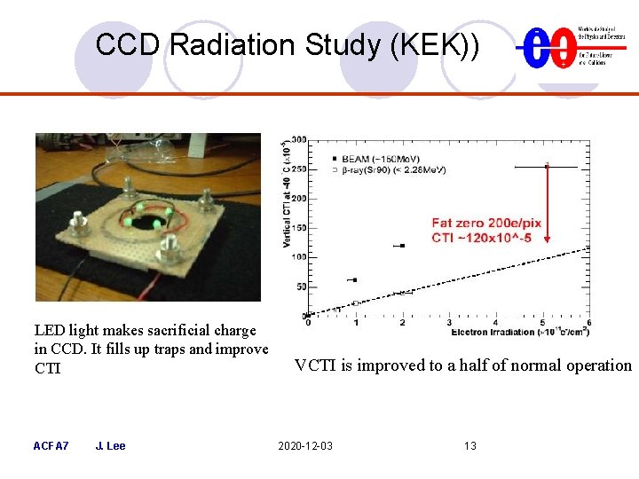
CCD Radiation Study (KEK)) LED light makes sacrificial charge in CCD. It fills up traps and improve CTI ACFA 7 J. Lee VCTI is improved to a half of normal operation 2020 -12 -03 13
CCD Summary • performance proven at SLD • good spacial resolution ( < 5µm) • improve slow readout speed 50 MHz CP readout • improve the radiation hardness charge injection, notch structure • material reduction with unsupported silicon ACFA 7 J. Lee 2020 -12 -03 14
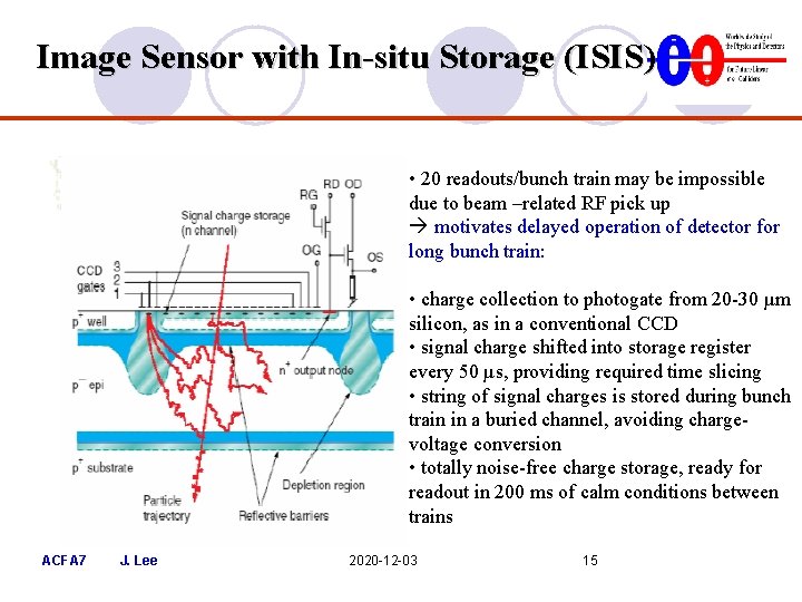
Image Sensor with In-situ Storage (ISIS) • 20 readouts/bunch train may be impossible due to beam –related RF pick up motivates delayed operation of detector for long bunch train: • charge collection to photogate from 20 -30 µm silicon, as in a conventional CCD • signal charge shifted into storage register every 50 µs, providing required time slicing • string of signal charges is stored during bunch train in a buried channel, avoiding chargevoltage conversion • totally noise-free charge storage, ready for readout in 200 ms of calm conditions between trains ACFA 7 J. Lee 2020 -12 -03 15
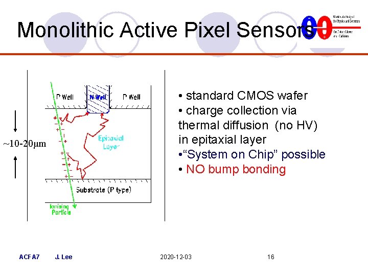
Monolithic Active Pixel Sensors • standard CMOS wafer • charge collection via thermal diffusion (no HV) in epitaxial layer • “System on Chip” possible • NO bump bonding ~10 -20µm ACFA 7 J. Lee 2020 -12 -03 16
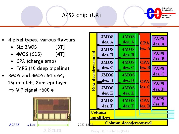
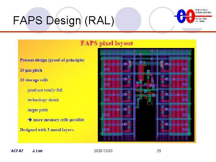
• 4 pixel types, various flavours • Std 3 MOS [3 T] • 4 MOS (CDS) [4 T] • CPA (charge amp) • FAPS (10 deep pipeline) • 3 MOS and 4 MOS: 64 x 64, 15 m pitch, 8 m epi-layer MIP signal ~600 e- ACFA 7 J. Lee 5. 8 mm Row decoder/control APS 2 chip (UK) 3 MOS des. A 4 MOS des. A 3 MOS des. B 4 MOS des. B 3 MOS des. C 4 MOS des. C 3 MOS des. D 4 MOS des. D 3 MOS des. E FAPS CPA des. A FAPS des. B CPA des. B FAPS des. C CPA FAPS des. C 4 MOS des. D des. E 4 MOS CPA FAPS des. F des. D des. E 3 MOS des. F Column amplifiers Column decoder/control 2020 -12 -03 17 Design: R. Turchetta (RAL)
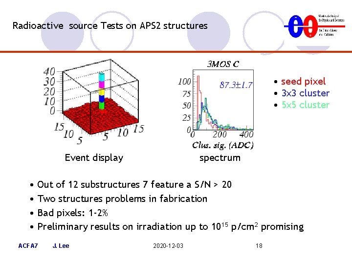
Radioactive source Tests on APS 2 structures • seed pixel • 3 x 3 cluster • 5 x 5 cluster Event display spectrum • Out of 12 substructures 7 feature a S/N > 20 • Two structures problems in fabrication • Bad pixels: 1 -2% • Preliminary results on irradiation up to 1015 p/cm 2 promising ACFA 7 J. Lee 2020 -12 -03 18
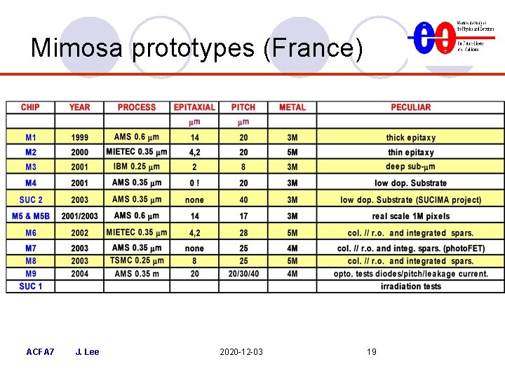
Mimosa prototypes (France) ACFA 7 J. Lee 2020 -12 -03 19
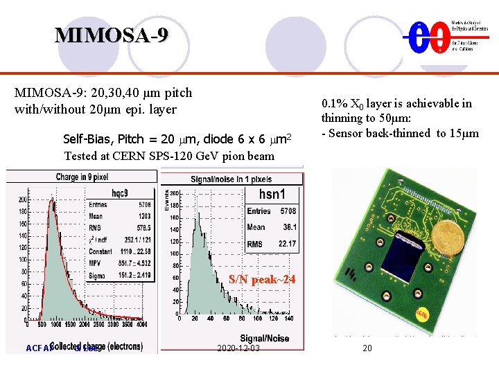
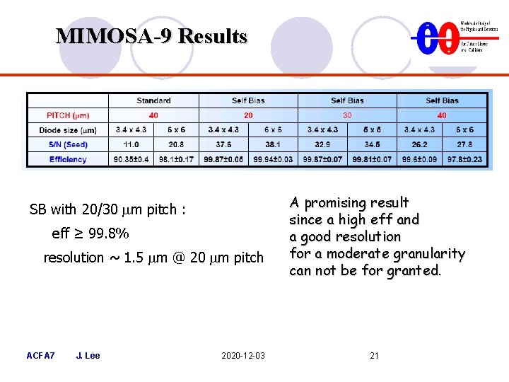
MIMOSA-9: 20, 30, 40 µm pitch with/without 20µm epi. layer Self-Bias, Pitch = 20 m, diode 6 x 6 m 2 Tested at CERN SPS-120 Ge. V pion beam 0. 1% X 0 layer is achievable in thinning to 50µm: - Sensor back-thinned to 15µm S/N peak~24 ACFA 7 J. Lee 2020 -12 -03 20
MIMOSA-9 Results SB with 20/30 m pitch : eff ≥ 99. 8% resolution ~ 1. 5 m @ 20 m pitch ACFA 7 J. Lee 2020 -12 -03 A promising result since a high eff and a good resolution for a moderate granularity can not be for granted. 21
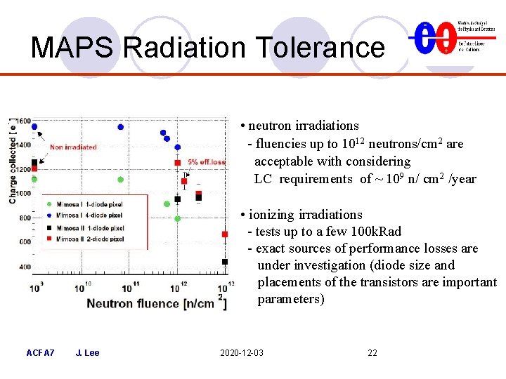
MAPS Radiation Tolerance • neutron irradiations - fluencies up to 1012 neutrons/cm 2 are acceptable with considering LC requirements of ~ 109 n/ cm 2 /year • ionizing irradiations - tests up to a few 100 k. Rad - exact sources of performance losses are under investigation (diode size and placements of the transistors are important parameters) ACFA 7 J. Lee 2020 -12 -03 22
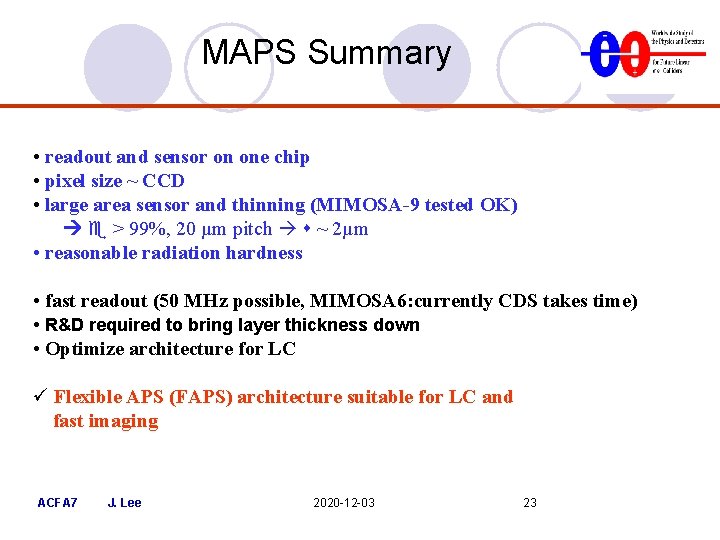
MAPS Summary • readout and sensor on one chip • pixel size ~ CCD • large area sensor and thinning (MIMOSA-9 tested OK) > 99%, 20 µm pitch ~ 2µm • reasonable radiation hardness • fast readout (50 MHz possible, MIMOSA 6: currently CDS takes time) • R&D required to bring layer thickness down • Optimize architecture for LC ü Flexible APS (FAPS) architecture suitable for LC and fast imaging ACFA 7 J. Lee 2020 -12 -03 23
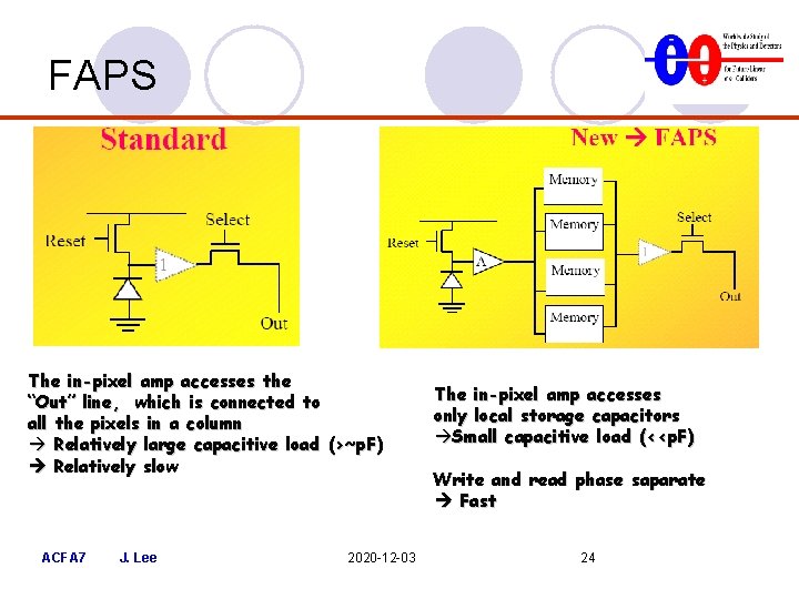
FAPS The in-pixel amp accesses the “Out” line, which is connected to all the pixels in a column Relatively large capacitive load (>~p. F) Relatively slow ACFA 7 J. Lee 2020 -12 -03 The in-pixel amp accesses only local storage capacitors Small capacitive load (<<p. F) Write and read phase saparate Fast 24
FAPS Design (RAL) ACFA 7 J. Lee 2020 -12 -03 25
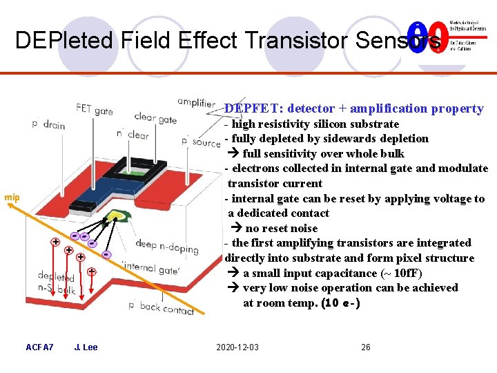
DEPleted Field Effect Transistor Sensors DEPFET: detector + amplification property mip + ACFA 7 -+ + + J. Lee - high resistivity silicon substrate - fully depleted by sidewards depletion full sensitivity over whole bulk - electrons collected in internal gate and modulate transistor current - internal gate can be reset by applying voltage to a dedicated contact no reset noise - the first amplifying transistors are integrated directly into substrate and form pixel structure a small input capacitance (~ 10 f. F) very low noise operation can be achieved at room temp. (10 e-) 2020 -12 -03 26
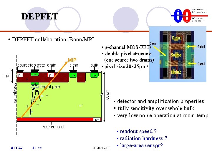
DEPFET • DEPFET collaboration: Bonn/MPI MIP p+ symmetry axis ~1µm n+ p+ p n - -+ gate -- internal -+ -+ + - clear bulk n+ n+ 50 µm source top gate drain • p-channel MOS-FETs • double pixel structure (one source two drains) • pixel size 20 x 25µm 2 n- p+ rear contact ACFA 7 J. Lee 2020 -12 -03 ▪ detector and amplification properties ▪ fully sensitivity over whole bulk ▪ very low noise operation at room temp. ▪ readout speed ? ▪ radiation hardness ? ▪ large-area sensor? 27
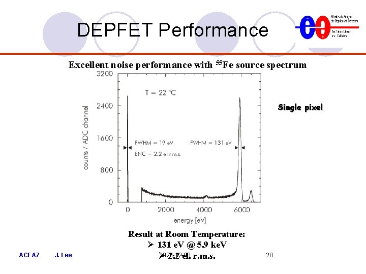
DEPFET Performance Excellent noise performance with 55 Fe source spectrum Single pixel ACFA 7 J. Lee Result at Room Temperature: Ø 131 e. V @ 5. 9 ke. V 2020 -12 -03 Ø 2. 2 el. r. m. s. 28
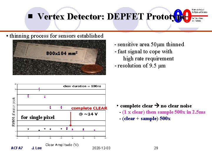
▣ Vertex Detector: DEPFET Prototype • thinning process for sensors established - sensitive area 50µm thinned - fast signal to cope with high rate requirement - resolution of 9. 5 µm 800 x 104 mm 2 • complete clear no clear noise - (1 x clear) then sample 500 x in 2. 5 ms - (clear + sample) 500 x for single pixel ACFA 7 J. Lee 2020 -12 -03 29
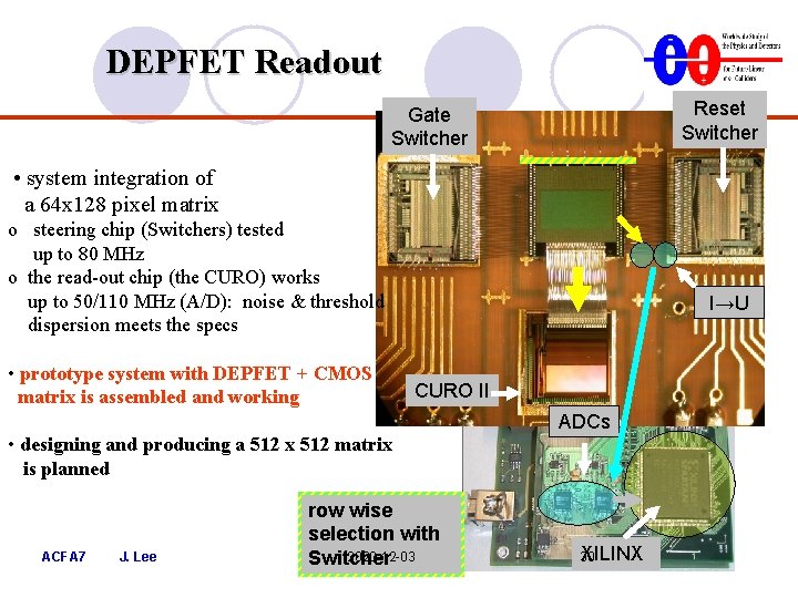
DEPFET Readout Reset Switcher Gate Switcher • system integration of a 64 x 128 pixel matrix o steering chip (Switchers) tested up to 80 MHz o the read-out chip (the CURO) works up to 50/110 MHz (A/D): noise & threshold dispersion meets the specs • prototype system with DEPFET + CMOS matrix is assembled and working I→U CURO II ADCs • designing and producing a 512 x 512 matrix is planned ACFA 7 J. Lee row wise selection with 2020 -12 -03 Switcher XILINX 30
DEPFET Summary • excellent low noise performance at room temperature • low power consumption (saving material for cooling structure) • readout speed increasing • possibilities of thinning the sensor (20 -30 μm) and readout chip • minimize pixel size • radiation hardness ACFA 7 J. Lee 2020 -12 -03 31
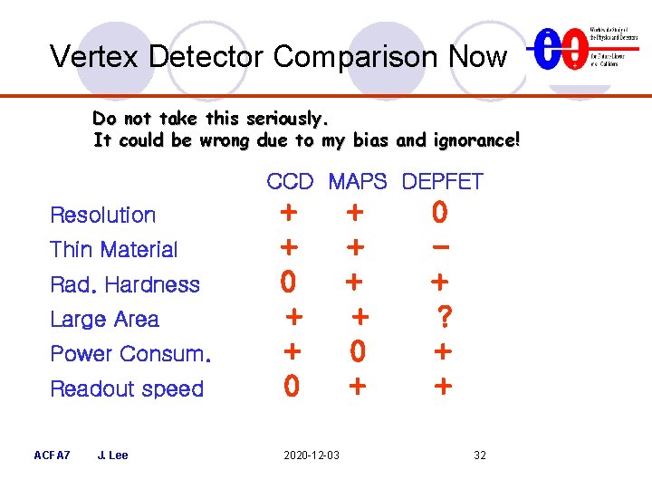
Vertex Detector Comparison Now Do not take this seriously. It could be wrong due to my bias and ignorance! CCD MAPS DEPFET Resolution Thin Material Rad. Hardness Large Area Power Consum. Readout speed ACFA 7 J. Lee + + 0 2020 -12 -03 + + 0 + ? + + 32
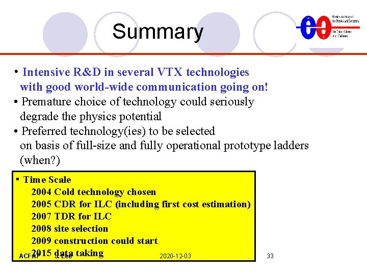
Summary • Intensive R&D in several VTX technologies with good world-wide communication going on! • Premature choice of technology could seriously degrade the physics potential • Preferred technology(ies) to be selected on basis of full-size and fully operational prototype ladders (when? ) ▪ Time Scale 2004 Cold technology chosen 2005 CDR for ILC (including first cost estimation) 2007 TDR for ILC 2008 site selection 2009 construction could start 2015 data ACFA 7 J. Lee taking 2020 -12 -03 33
backups ACFA 7 J. Lee 2020 -12 -03 34
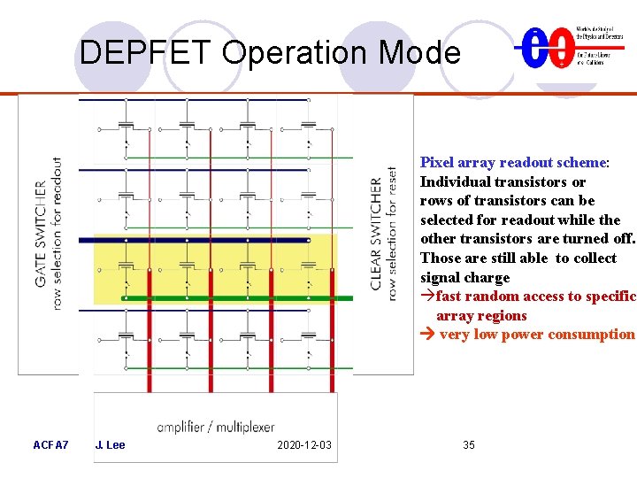
DEPFET Operation Mode Pixel array readout scheme: Individual transistors or rows of transistors can be selected for readout while the other transistors are turned off. Those are still able to collect signal charge fast random access to specific array regions very low power consumption ACFA 7 J. Lee 2020 -12 -03 35
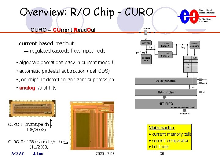
Overview: R/O Chip - CURO – CUrrent Read. Out current based readout → regulated cascode fixes input node • algebraic operations easy in current mode ! • automatic pedestal subtraction (fast CDS) • „on chip“ hit detection and zero suppression • analog r/o of hits CURO I: prototype chip (05/2002) Main parts : • current memory cells • current comparator • hit finder CURO II: 128 channel r/o chip (11/2003) ACFA 7 J. Lee 2020 -12 -03 36