
Response time of Alkali Antimonides John Smedley Brookhaven
Response time of Alkali Antimonides John Smedley Brookhaven National Laboratory

Overview • The Three-Step Model and Response Time – Metallic Photocathodes – Semiconductor Photocathodes • Positive Electron Affinity (Alkali Antimonide) • Negative Electron Affinity (Cs: Ga. As) • Diamond Electron Amplifier Modern Theory and Applications of Photocathodes W. E. Spicer & A. Herrera-Gómez SAC-PUB-6306 (1993)
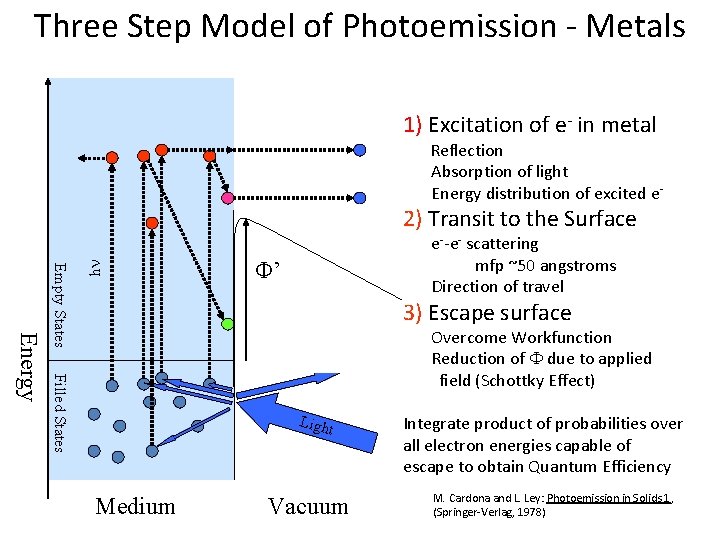
Three Step Model of Photoemission - Metals 1) Excitation of e- in metal Reflection Absorption of light Energy distribution of excited ee--e- scattering mfp ~50 angstroms Direction of travel Φ Φ’ Φ 3) Escape surface Overcome Workfunction Reduction of due to applied field (Schottky Effect) Filled States Energy Empty States h Vacuum level 2) Transit to the Surface Ligh t Medium Vacuum Integrate product of probabilities over all electron energies capable of escape to obtain Quantum Efficiency M. Cardona and L. Ley: Photoemission in Solids 1, (Springer-Verlag, 1978)
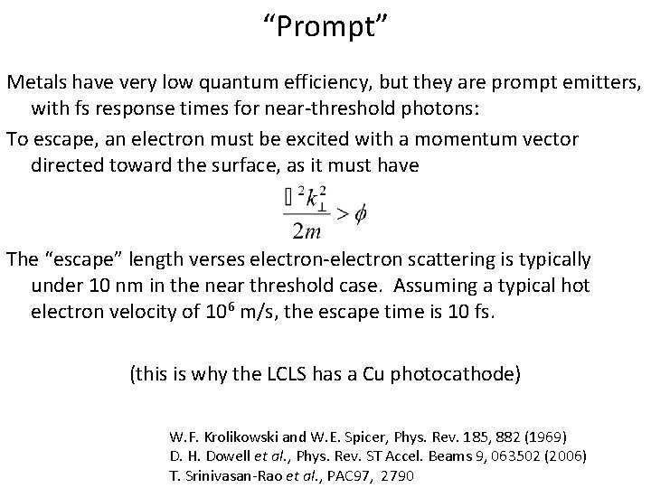
“Prompt” Metals have very low quantum efficiency, but they are prompt emitters, with fs response times for near-threshold photons: To escape, an electron must be excited with a momentum vector directed toward the surface, as it must have The “escape” length verses electron-electron scattering is typically under 10 nm in the near threshold case. Assuming a typical hot electron velocity of 106 m/s, the escape time is 10 fs. (this is why the LCLS has a Cu photocathode) W. F. Krolikowski and W. E. Spicer, Phys. Rev. 185, 882 (1969) D. H. Dowell et al. , Phys. Rev. ST Accel. Beams 9, 063502 (2006) T. Srinivasan-Rao et al. , PAC 97, 2790
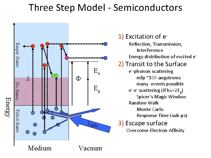
Three Step Model - Semiconductors 1) Excitation of e- h Empty States Reflection, Transmission, Interference Energy distribution of excited e- Eg Filled States Energy No States Φ Ea Ligh t Medium Vacuum 2) Transit to the Surface e--phonon scattering mfp ~100 angstroms many events possible e--e- scattering (if hν>2 Eg) Spicer’s Magic Window Random Walk Monte Carlo Response Time (sub-ps) 3) Escape surface Overcome Electron Affinity
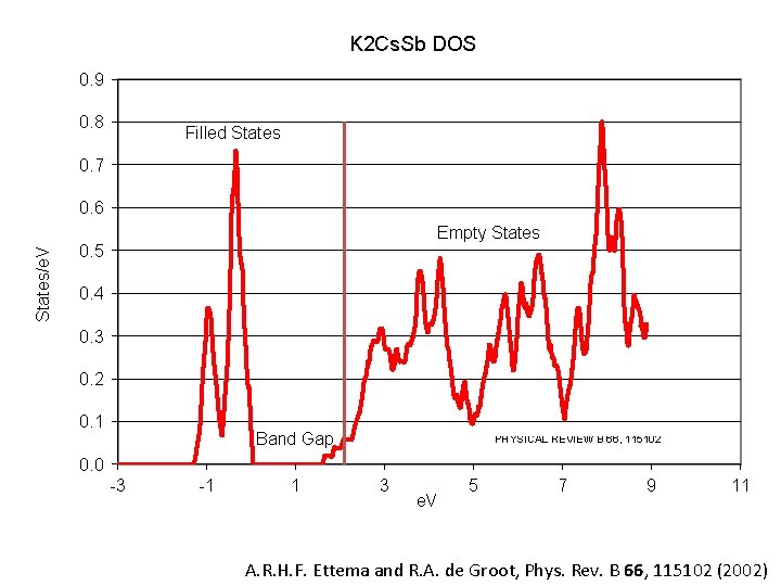
K 2 Cs. Sb DOS 0. 9 0. 8 Filled States 0. 7 States/e. V 0. 6 Empty States 0. 5 0. 4 0. 3 0. 2 0. 1 Band Gap PHYSICAL REVIEW B 66, 115102 0. 0 -3 -1 1 3 e. V 5 7 9 11 A. R. H. F. Ettema and R. A. de Groot, Phys. Rev. B 66, 115102 (2002)
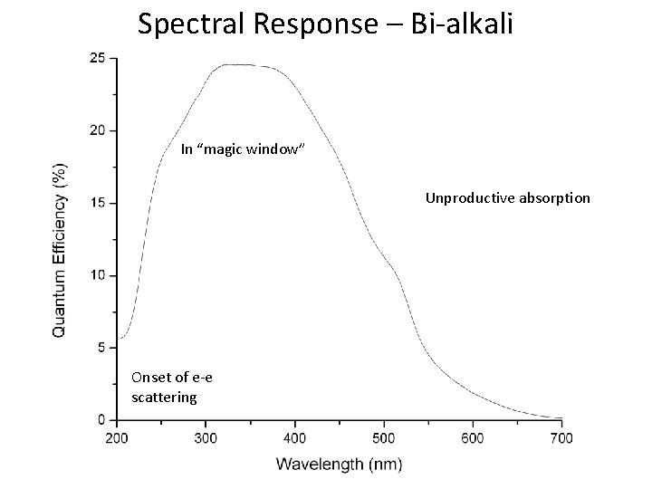
Spectral Response – Bi-alkali In “magic window” Unproductive absorption Onset of e-e scattering
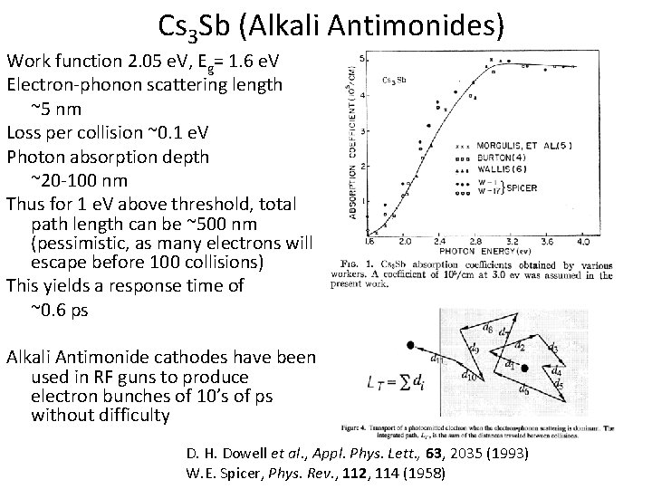
Cs 3 Sb (Alkali Antimonides) Work function 2. 05 e. V, Eg= 1. 6 e. V Electron-phonon scattering length ~5 nm Loss per collision ~0. 1 e. V Photon absorption depth ~20 -100 nm Thus for 1 e. V above threshold, total path length can be ~500 nm (pessimistic, as many electrons will escape before 100 collisions) This yields a response time of ~0. 6 ps Alkali Antimonide cathodes have been used in RF guns to produce electron bunches of 10’s of ps without difficulty D. H. Dowell et al. , Appl. Phys. Lett. , 63, 2035 (1993) W. E. Spicer, Phys. Rev. , 112, 114 (1958)
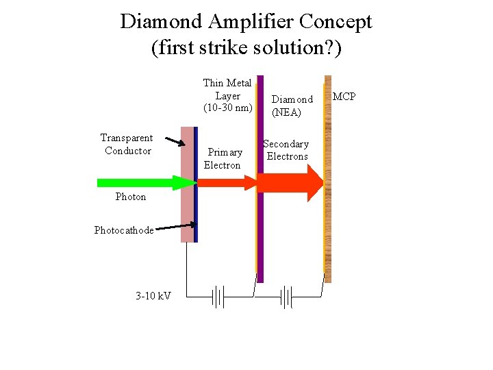
Diamond Amplifier Concept (first strike solution? ) Thin Metal Layer (10 -30 nm) Transparent Conductor Photon Photocathode 3 -10 k. V Primary Electron Diamond (NEA) Secondary Electrons MCP
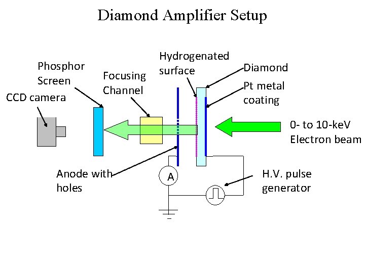
Diamond Amplifier Setup Phosphor Screen CCD camera Focusing Channel Hydrogenated surface Diamond Pt metal coating 0 - to 10 -ke. V Electron beam Anode with holes A H. V. pulse generator
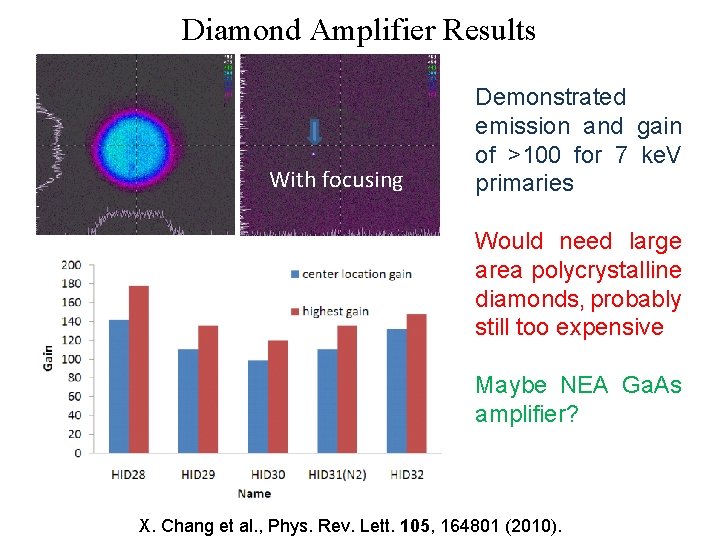
Diamond Amplifier Results With focusing Demonstrated emission and gain of >100 for 7 ke. V primaries Would need large area polycrystalline diamonds, probably still too expensive Maybe NEA Ga. As amplifier? X. Chang et al. , Phys. Rev. Lett. 105, 164801 (2010).
Closing Thoughts While not strictly “prompt” in the manner of metals, the alkali atimonides have sub-ps response time Could be improved to some extent (at the cost of QE) by making the cathode very thin Electron stimulated desorption/Ion backbombardment? Thanks! D. Dowell (SLAC/LCLS), Henry & Klaus for the invitation; V. Radeka, I. Ben-Zvi, and my colleagues at BNL
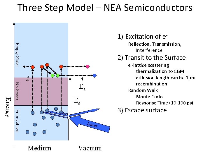
Three Step Model – NEA Semiconductors 1) Excitation of e. Empty States Reflection, Transmission, Interference 2) Transit to the Surface h e--lattice scattering thermalization to CBM diffusion length can be 1µm recombination Random Walk Monte Carlo Response Time (10 -100 ps) Eg 3) Escape surface Filled States Energy No States Ea Lase r Medium Vacuum
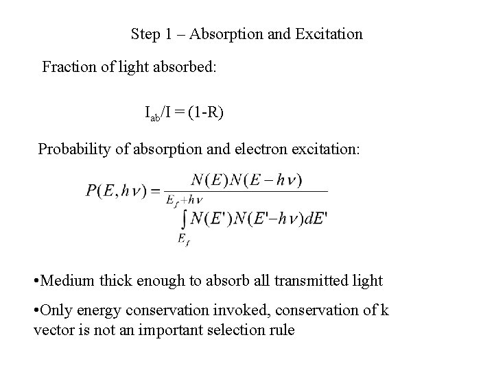
Step 1 – Absorption and Excitation Fraction of light absorbed: Iab/I = (1 -R) Probability of absorption and electron excitation: • Medium thick enough to absorb all transmitted light • Only energy conservation invoked, conservation of k vector is not an important selection rule
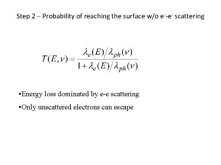
Step 2 – Probability of reaching the surface w/o e--e- scattering • Energy loss dominated by e-e scattering • Only unscattered electrons can escape
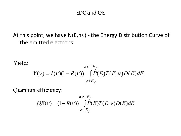
EDC and QE At this point, we have N(E, h ) - the Energy Distribution Curve of the emitted electrons Yield: Quantum efficiency:
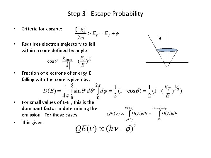
Step 3 - Escape Probability • Criteria for escape: • Requires electron trajectory to fall within a cone defined by angle: • Fraction of electrons of energy E falling with the cone is given by: • For small values of E-ET, this is the dominant factor in determining the emission. For these cases: This gives: •
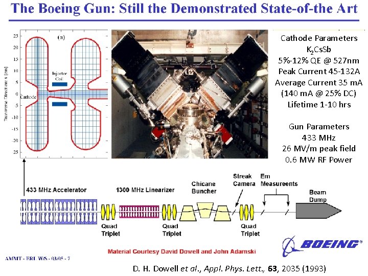
Cathode Parameters K 2 Cs. Sb 5%-12% QE @ 527 nm Peak Current 45 -132 A Average Current 35 m. A (140 m. A @ 25% DC) Lifetime 1 -10 hrs Gun Parameters 433 MHz 26 MV/m peak field 0. 6 MW RF Power D. H. Dowell et al. , Appl. Phys. Lett. , 63, 2035 (1993)
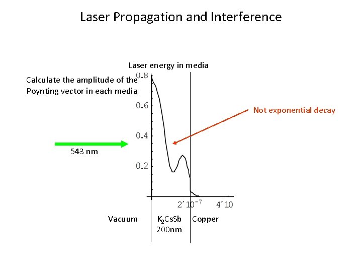
Laser Propagation and Interference Laser energy in media Calculate the amplitude of the Poynting vector in each media Not exponential decay 543 nm Vacuum K 2 Cs. Sb 200 nm Copper

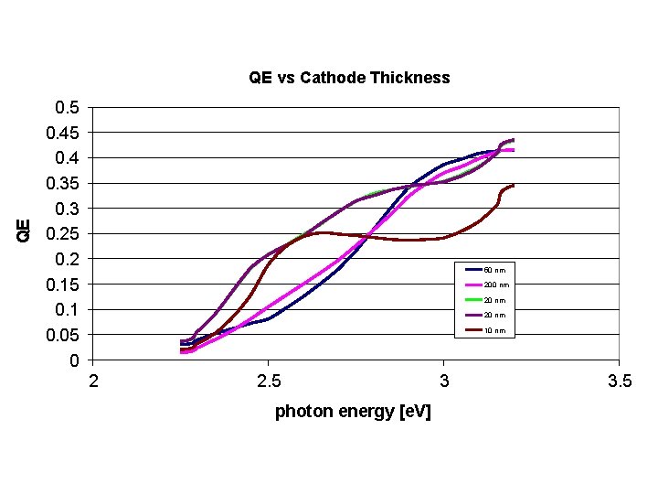
QE QE vs Cathode Thickness 0. 5 0. 4 0. 35 0. 3 0. 25 0. 2 0. 15 0. 1 0. 05 0 50 nm 20 nm 10 nm 2 2. 5 photon energy [e. V] 3 3. 5
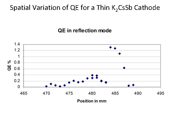
Spatial Variation of QE for a Thin K 2 Cs. Sb Cathode
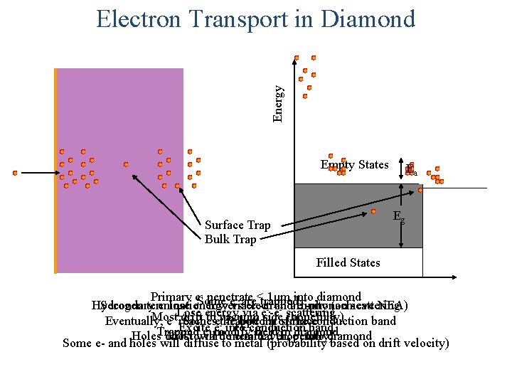
Energy Electron Transport in Diamond Empty States Ea Eg Surface Trap Bulk Trap Filled States - penetrate < 1μm into diamond Primary e. Some - are trapped evia Hydrogen Secondary termination e lose energy lowers electron e--e-- and affinity e--phonon (achieve scattering NEA) Lose energy via e -e scattering Most drift side (hopefully) - trapped Eventually, e- reaches Sometoevacuum the bottom at of surface the conduction band Excite e into conduction band e modify field in ediamond - into diamond Holes. Trapped drift Mosttoward will bemetal emitted layer, (hopefully) Some e- and holes will diffuse to metal (probability based on drift velocity)
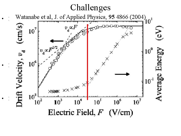
Challenges Watanabe et al, J. of Applied Physics, 95 4866 (2004) • Electrons must escape diamond – Diamond must <30 μm for 700 MHz RF – Negative Electron Affinity (NEA) surface for emission – Field in the diamond is a critical parameter • Field should be high enough for ve to saturate • Field should be low enough to minimize e- energy • Modeling suggests 3 MV/m – good for SRF injector • Diamond must not accumulate charge – Material must have a minimum of bulk/surface traps – Stimulated detrapping – Metal layer required to neutralize holes • Minimize energy loss in metal (low Z, low ρ) • Practical aspects – Electron stimulated desorption – Heat load and thermal stresses (1100 K to 77 K) – Effect of ion/electron back-bombardment on H-terminated surface
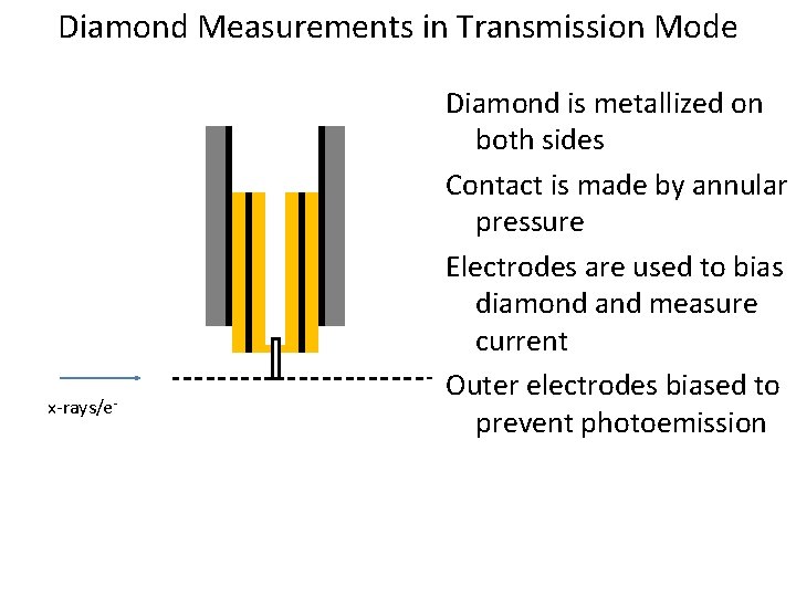
Diamond Measurements in Transmission Mode x-rays/e- Diamond is metallized on both sides Contact is made by annular pressure Electrodes are used to bias diamond and measure current Outer electrodes biased to prevent photoemission
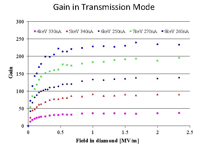
Gain in Transmission Mode 300 4 ke. V 330 n. A 5 ke. V 340 n. A 6 ke. V 250 n. A 7 ke. V 270 n. A 8 ke. V 260 n. A 250 Gain 200 150 100 50 0 0 0. 5 1 1. 5 Field in diamond [MV/m] 2 2. 5
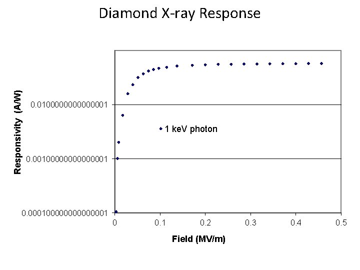
Responsivity (A/W) Diamond X-ray Response 0. 0100000001 1 ke. V photon 0. 00100000001 0. 000100000001 0 0. 1 0. 2 Field (MV/m) 0. 3 0. 4 0. 5
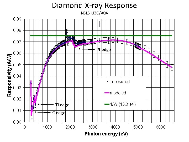
Diamond X-ray Response NSLS U 3 C/X 8 A 0. 09 0. 08 Responsivity (A/W) 0. 07 Pt edge 0. 06 0. 05 0. 04 measured 0. 03 modeled 0. 02 1/W (13. 3 e. V) Ti edge 0. 01 C edge 0. 00 0 1000 2000 3000 4000 Photon energy (e. V) 5000 6000
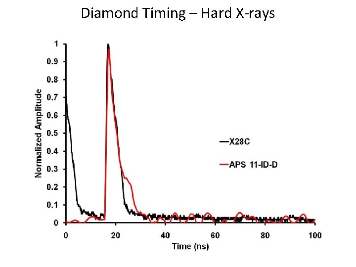
Diamond Timing – Hard X-rays
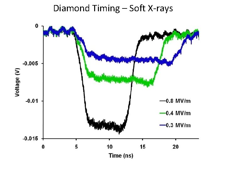
Diamond Timing – Soft X-rays
- Slides: 30