Research Interests generally application of physical crystallography to
- Slides: 4

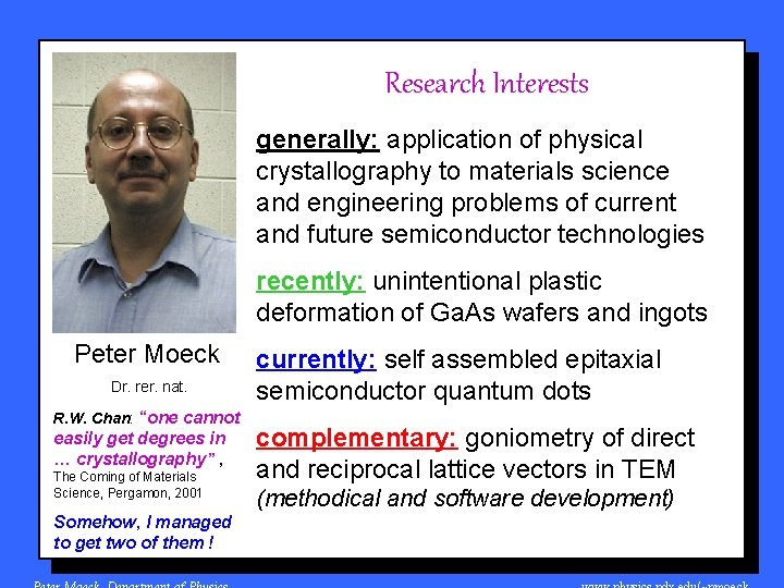
Research Interests generally: application of physical crystallography to materials science and engineering problems of current and future semiconductor technologies recently: unintentional plastic deformation of Ga. As wafers and ingots Peter Moeck Dr. rer. nat. R. W. Chan: “one cannot easily get degrees in … crystallography” , The Coming of Materials Science, Pergamon, 2001 Somehow, I managed to get two of them ! currently: self assembled epitaxial semiconductor quantum dots complementary: goniometry of direct and reciprocal lattice vectors in TEM (methodical and software development)

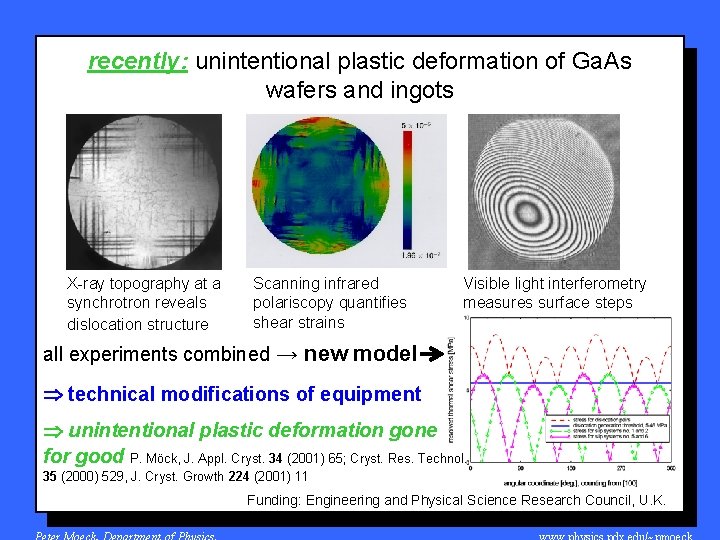
recently: unintentional plastic deformation of Ga. As wafers and ingots X-ray topography at a synchrotron reveals dislocation structure Scanning infrared polariscopy quantifies shear strains Visible light interferometry measures surface steps all experiments combined → new model technical modifications of equipment unintentional plastic deformation gone for good P. Möck, J. Appl. Cryst. 34 (2001) 65; Cryst. Res. Technol. 35 (2000) 529, J. Cryst. Growth 224 (2001) 11 Funding: Engineering and Physical Science Research Council, U. K.

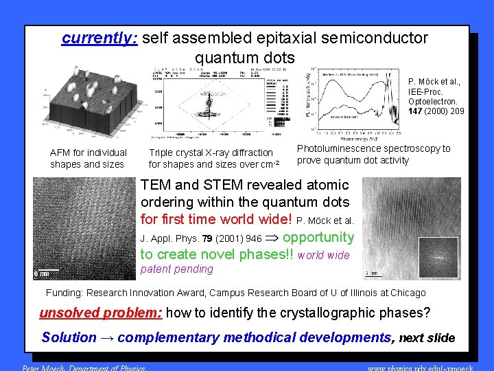
currently: self assembled epitaxial semiconductor quantum dots P. Möck et al. , IEE-Proc. Optoelectron. 147 (2000) 209 AFM for individual shapes and sizes Triple crystal X-ray diffraction for shapes and sizes over cm-2 Photoluminescence spectroscopy to prove quantum dot activity TEM and STEM revealed atomic ordering within the quantum dots for first time world wide! P. Möck et al. J. Appl. Phys. 79 (2001) 946 opportunity to create novel phases!! world wide patent pending Funding: Research Innovation Award, Campus Research Board of U of Illinois at Chicago unsolved problem: how to identify the crystallographic phases? Solution → complementary methodical developments, next slide

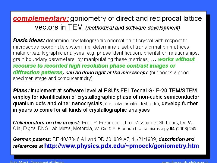
complementary: goniometry of direct and reciprocal lattice vectors in TEM (methodical and software development) Basic Ideas: determine crystallographic orientation of crystal with respect to microscope coordinate system, i. e. determine a set of transformation matrices, make crystallographic analyses, e. g. phase identification, orientation relationships, grain boundary parameters, by manipulating these matrices, … works without recourse to recorded high resolution phase contrast images or diffraction patterns, can be done right at the microscope (but needs a good specimen stage and compucentricity) Plans: implement at software level at PSU’s FEI Tecnai G 2 F-20 TEM/STEM, employ for identification of crystallographic phase of non-cubic semiconductor quantum dots and other nanocrystals, (i. e. solve problem last slide), develop further in years to come for all kinds of crystallographic analyses Collaborators on this project: Prof. P. Fraundorf, U. of Missouri at St. Louis, Dr. W. Qin, Digital DNS Lab Meza, Motorola, W. Qin & P. Fraundorf, Ultramicroscopy 94 (2003) 245 German patents: DE 4037346 A 1 and DD 301839 A 7, 11/21/1989, description and references at http: //www. physics. pdx. edu/~pmoeck/goniometry. htm