Report from CMOS WG 1 Interesting Foundries and
- Slides: 20

Report from CMOS WG 1 Interesting Foundries and State of Submissions Efficiency and Noise Occupancy Single Pixel Design Reticle Architectures Module Architectures Material Estimates Plans on how to proceed 1

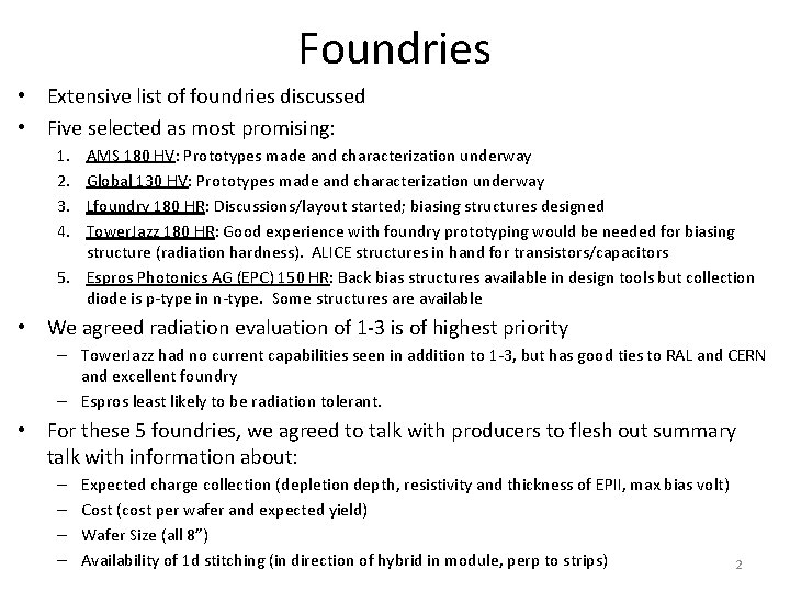
Foundries • Extensive list of foundries discussed • Five selected as most promising: 1. 2. 3. 4. AMS 180 HV: Prototypes made and characterization underway Global 130 HV: Prototypes made and characterization underway Lfoundry 180 HR: Discussions/layout started; biasing structures designed Tower. Jazz 180 HR: Good experience with foundry prototyping would be needed for biasing structure (radiation hardness). ALICE structures in hand for transistors/capacitors 5. Espros Photonics AG (EPC) 150 HR: Back bias structures available in design tools but collection diode is p-type in n-type. Some structures are available • We agreed radiation evaluation of 1 -3 is of highest priority – Tower. Jazz had no current capabilities seen in addition to 1 -3, but has good ties to RAL and CERN and excellent foundry – Espros least likely to be radiation tolerant. • For these 5 foundries, we agreed to talk with producers to flesh out summary talk with information about: – – Expected charge collection (depletion depth, resistivity and thickness of EPII, max bias volt) Cost (cost per wafer and expected yield) Wafer Size (all 8”) Availability of 1 d stitching (in direction of hybrid in module, perp to strips) 2

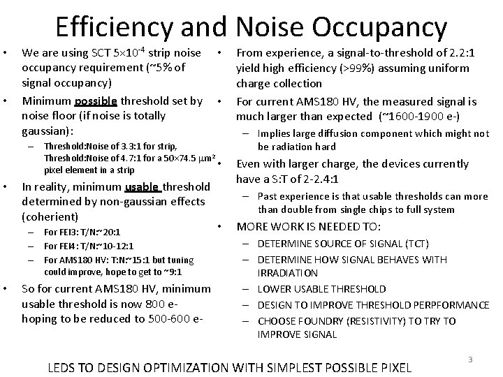
Efficiency and Noise Occupancy • • We are using SCT 5× 10 -4 strip noise occupancy requirement (~5% of signal occupancy) Minimum possible threshold set by noise floor (if noise is totally gaussian): • • – Threshold: Noise of 3. 3: 1 for strip, Threshold: Noise of 4. 7: 1 for a 50× 74. 5 mm 2 • pixel element in a strip • In reality, minimum usable threshold determined by non-gaussian effects (coherient) – For FEI 3: T/N: ~20: 1 – For FEI 4: T/N: ~10 -12: 1 – For AMS 180 HV: T: N: ~15: 1 but tuning could improve, hope to get to ~9: 1 • So for current AMS 180 HV, minimum usable threshold is now 800 ehoping to be reduced to 500 -600 e- From experience, a signal-to-threshold of 2. 2: 1 yield high efficiency (>99%) assuming uniform charge collection For current AMS 180 HV, the measured signal is much larger than expected (~1600 -1900 e-) – Implies large diffusion component which might not be radiation hard Even with larger charge, the devices currently have a S: T of 2 -2. 4: 1 – Past experience is that usable thresholds can more than double from single chips to full system • MORE WORK IS NEEDED TO: – DETERMINE SOURCE OF SIGNAL (TCT) – DETERMINE HOW SIGNAL BEHAVES WITH IRRADIATION – LOWER USABLE THRESHOLD – DESIGN TO IMPROVE THRESHOLD PERPFORMANCE – CHOOSE FOUNDRY (RESISTIVITY) TO TRY TO IMPROVE SIGNAL LEDS TO DESIGN OPTIMIZATION WITH SIMPLEST POSSIBLE PIXEL 3

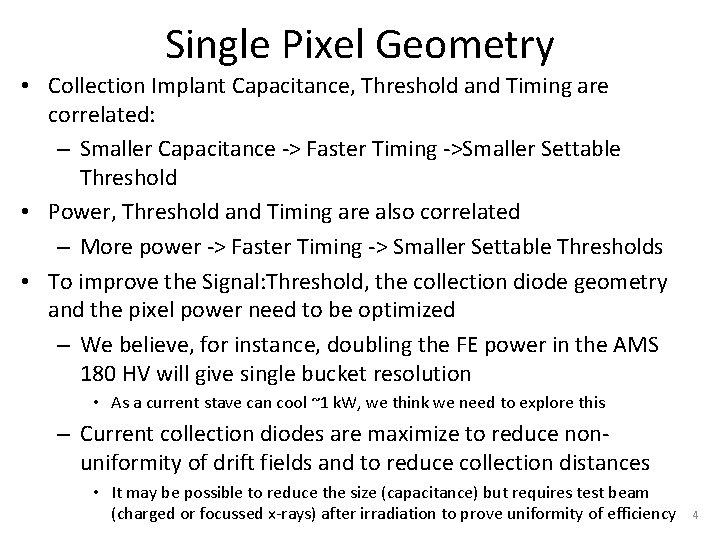
Single Pixel Geometry • Collection Implant Capacitance, Threshold and Timing are correlated: – Smaller Capacitance -> Faster Timing ->Smaller Settable Threshold • Power, Threshold and Timing are also correlated – More power -> Faster Timing -> Smaller Settable Thresholds • To improve the Signal: Threshold, the collection diode geometry and the pixel power need to be optimized – We believe, for instance, doubling the FE power in the AMS 180 HV will give single bucket resolution • As a current stave can cool ~1 k. W, we think we need to explore this – Current collection diodes are maximize to reduce nonuniformity of drift fields and to reduce collection distances • It may be possible to reduce the size (capacitance) but requires test beam (charged or focussed x-rays) after irradiation to prove uniformity of efficiency 4

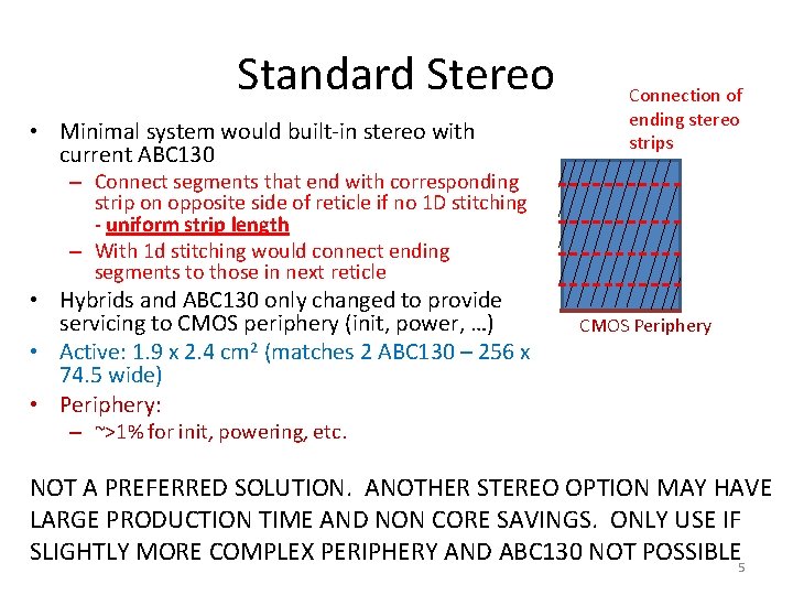
Standard Stereo • Minimal system would built-in stereo with current ABC 130 Connection of ending stereo strips – Connect segments that end with corresponding strip on opposite side of reticle if no 1 D stitching - uniform strip length – With 1 d stitching would connect ending segments to those in next reticle • Hybrids and ABC 130 only changed to provide servicing to CMOS periphery (init, power, …) • Active: 1. 9 x 2. 4 cm 2 (matches 2 ABC 130 – 256 x 74. 5 wide) • Periphery: CMOS Periphery – ~>1% for init, powering, etc. NOT A PREFERRED SOLUTION. ANOTHER STEREO OPTION MAY HAVE LARGE PRODUCTION TIME AND NON CORE SAVINGS. ONLY USE IF SLIGHTLY MORE COMPLEX PERIPHERY AND ABC 130 NOT POSSIBLE 5

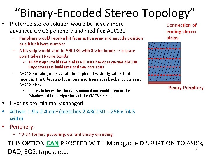
“Binary-Encoded Stereo Topology” • Preferred stereo solution would be have a more advanced CMOS periphery and modified ABC 130 – Periphery would receive hit from active area and encode position as a 8 bit binary number – A hit strip would sent to ABC 130 with 8 wire bonds -> a space point takes 16 wire bonds Connection of ending stereo strips • 16 hit strips would take ½ of the FE wire bonds as current ABC 130. Huge savings in build time and non-core costs – ABC 130 analogue FE would be replaced with digital FE that receives the 8 bit strip locations and translates back into current ABC 130 BE. • Francis believes this change is minimal and could occur in the “shadow” of the design study of the CMOS sensor Binary Periphery • Hybrids are minimally changed • Active: 1. 9 x 2. 4 cm 2 (matches 2 ABC 130 – 256 x 74. 5 wide) • Periphery: – ~3 -5% for init, powering, etc and binary encoding THIS OPTION CAN PROCEED WITH Managable DISRUPTION TO ASICs, 6 DAQ, EOS, tapes, etc.

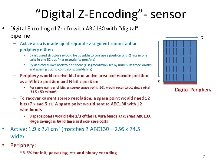
“Digital Z-Encoding”- sensor • Digital Encoding of Z-info with ABC 130 with “digital” pipeline X – Active area is made up of separate z-segment connected to periphery either: • • By a bussed structure (would be possible to confuse z position with 2 hits in one strip in one BC but finer granularity possible) By dedicated lines back to periphery (z-segmentation set by minimum trace widths and spacing but no confusion possible in z) – Periphery would receive hit from active area and encode position as a M bit x position and N bit z position • For same number of bits as stereo space point (16), would reconstruct single pixel (74. 5 x 50 micron 2) z Digital Periphery – To recover current stereo resolution, a space point would need 12 bits (7 x and 5 z). A space point would sent to ABC 130 with 12 wire bonds • 8 space points would take 1/3 of the FE wire bonds as current ABC 130. Huge savings in build time and non-core costs • Active: 1. 9 x 2. 4 cm 2 (matches 2 ABC 130 – 256 x 74. 5 wide) • Periphery: – ~3 -5% for init, powering, etc and binary encoding 7

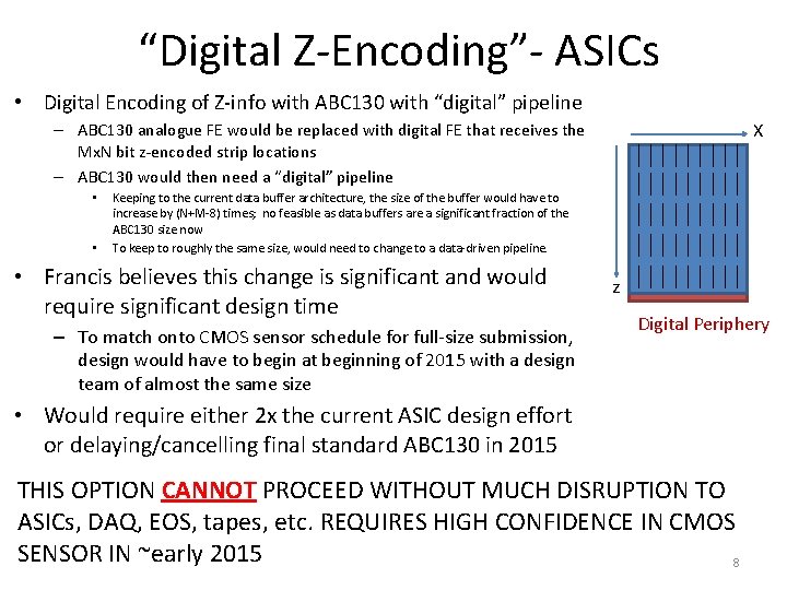
“Digital Z-Encoding”- ASICs • Digital Encoding of Z-info with ABC 130 with “digital” pipeline X – ABC 130 analogue FE would be replaced with digital FE that receives the Mx. N bit z-encoded strip locations – ABC 130 would then need a “digital” pipeline • • Keeping to the current data buffer architecture, the size of the buffer would have to increase by (N+M-8) times; no feasible as data buffers are a significant fraction of the ABC 130 size now To keep to roughly the same size, would need to change to a data-driven pipeline. • Francis believes this change is significant and would require significant design time – To match onto CMOS sensor schedule for full-size submission, design would have to begin at beginning of 2015 with a design team of almost the same size z Digital Periphery • Would require either 2 x the current ASIC design effort or delaying/cancelling final standard ABC 130 in 2015 THIS OPTION CANNOT PROCEED WITHOUT MUCH DISRUPTION TO ASICs, DAQ, EOS, tapes, etc. REQUIRES HIGH CONFIDENCE IN CMOS SENSOR IN ~early 2015 8

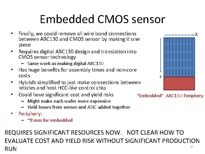
Embedded CMOS sensor • Finally, we could remove all wire bond connections between ABC 130 and CMOS sensor by making it one piece • Requires digital ABC 130 design and translation into CMOS sensor technology X – Same work as making digital ABC 130 • Has huge benefits for assembly times and non-core costs z • Hybrids simplified to just make connections between reticles and host HCC-like control chip • Could have significant cost and yield risks “Embedded” ABC 130 Periphery – Might make each wafer more expensive – Yield losses from sensor and ASIC added together • Periphery: – ~8 mm for embedded REQUIRES SIGNIFICANT RESOURCES NOW. NOT CLEAR HOW TO EVALUATE COST AND YIELD RISK WITHOUT SIGNIFICANT PRODUCTION 9 RUN

Discounted CMOS Architectures • True drop-in (no z-info) – Not likely to actualize cost saving with respect to planar unless sensor area halved – Would require periphery on other edge in order to not have larger dead regions • Analogue z-encoding – It is strongly believed digital encoding is much easier to achieve both in the CMOS sensor and the ABC 130 10

Outline of architecture program • Proceed assume binary-encoded stereo topology – Francis will look more into changes needed for digital pipeline for ABC 130 – Renato will look at design of periphery option – Further evaluations of current CMOS devices • If CMOS still looks promising and additional z-resolution is useful: – Go to Digital Z-Encoding if both Francis’s and Renato’s studies are positive – If periphery looks to difficult, drop back to standard stereo – Else stay with binary-encoded stereo topology • Assume embedded CMOS is not within time constraints or financial resources unless schedule and funding changes really soon 11

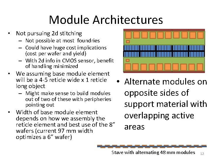
Module Architectures • Not pursuing 2 d stitching – Not possible at most foundries – Could have huge cost implications (cost per wafer and yield) – With 2 d info in CMOS sensor, benefit of handling minimized • We assuming base module element will be a 4 -5 reticle wide x 1 reticle long object • • Alternate modules on – Might make sense to build modules opposite sides of out of two of these with peripheries pointing out support material with Width of base module element overlapping active depends on how we assembly the reticle element and best use of the 8” areas wafers (current 97 mm width optimizes a 6” wafer) Stave with alternating 48 mm modules 12

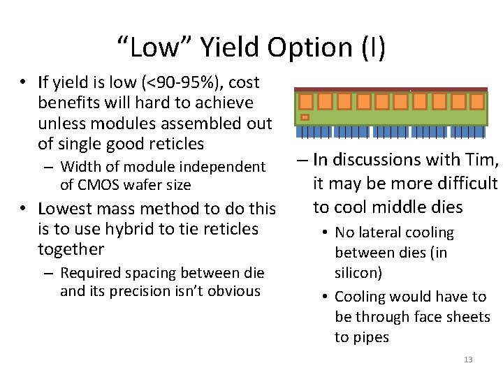
“Low” Yield Option (I) • If yield is low (<90 -95%), cost benefits will hard to achieve unless modules assembled out of single good reticles – Width of module independent of CMOS wafer size • Lowest mass method to do this is to use hybrid to tie reticles together – Required spacing between die and its precision isn’t obvious – In discussions with Tim, it may be more difficult to cool middle dies • No lateral cooling between dies (in silicon) • Cooling would have to be through face sheets to pipes 13

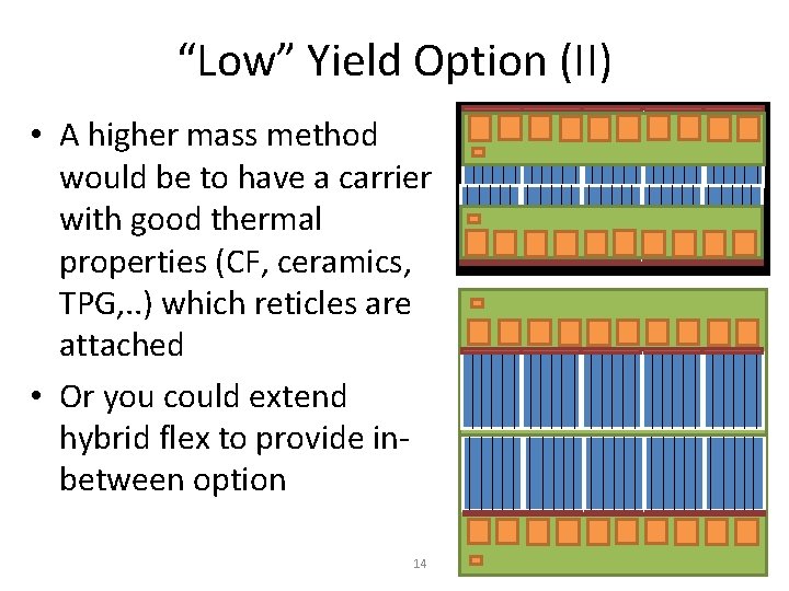
“Low” Yield Option (II) • A higher mass method would be to have a carrier with good thermal properties (CF, ceramics, TPG, . . ) which reticles are attached • Or you could extend hybrid flex to provide inbetween option 14

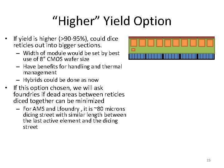
“Higher” Yield Option • If yield is higher (>90 -95%), could dice reticles out into bigger sections. – Width of module would be set by best use of 8” CMOS wafer size – Have benefits for handling and thermal management – Hybrids could be done as now • If this option chosen, we will ask foundries if dead areas between reticles diced together can be minimized – For AMS and Lfoundry , it is ~80 microns dicing street with similar length between the last active element and the dicing street 15

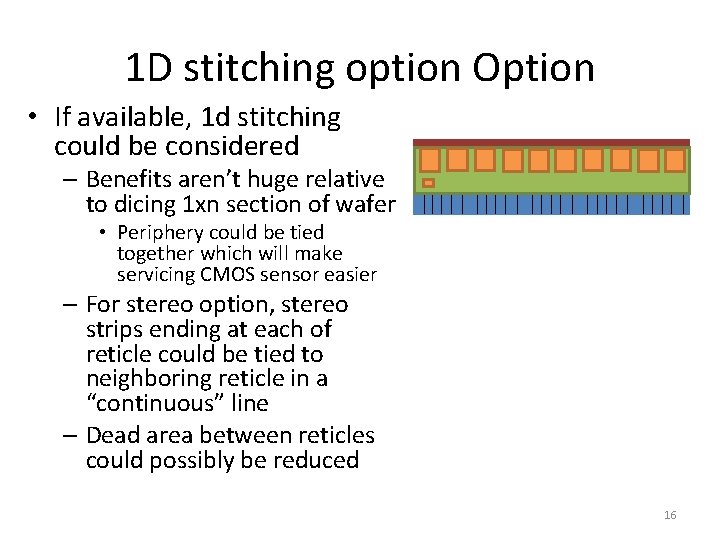
1 D stitching option Option • If available, 1 d stitching could be considered – Benefits aren’t huge relative to dicing 1 xn section of wafer • Periphery could be tied together which will make servicing CMOS sensor easier – For stereo option, stereo strips ending at each of reticle could be tied to neighboring reticle in a “continuous” line – Dead area between reticles could possibly be reduced 16

Radiation Length • Current radiation length of a stave – Cores (including tapes): 0. 72% – 2 Planar Modules: 1. 08% – Total: 1. 8% • For CMOS assume no additional material in carrier • Drop-in Stereo and Z-Encoded (100 micron thick sensors): – 1 Drop-in Module: 0. 31% – Total: 1. 03% • Embedded (100 micron thick sensors + hybrid width reduced by ASIC size): – 1 Embedded Module: 0. 25% – Total: 0. 97% It is possible that core can be reduced with CMOS sensors Most of material improvement made with going to single 17 modules with 2 d information

Current Priorities • Determining the radiation tolerance of CMOS devices is of highest priority – AMS 180 HV available now, imminent Lfoundry 150 HR submission important to explore higher resistivity material – It is not clear if this could be evaluated this year with current resources – It would be very useful if other groups could be involved • Requires FEI 4 and USBPIX experience • Available test program – Source tests can be made to give relative efficiency vs bias voltage measurement (hit rate vs bias) and some measure of signal – Diamond at RAL could give focussed x-rays to give relative efficiency within a cell – Test beams are needed for absolute efficiencies • DESY has no available slots this year • SLAC may be available in May • CERN PS may be available in Oct • Lack of test beams in this years appears to be a (the) critical item in the CMOS program Much more effort and resources are needed here to accelerate this evaluation. Without this ability, can not fulfil program in needed strip timescales 18

Schedule and Resources • CMOS program is still seen as a 3 submission program with (~>1 year per submission cycle) – Additional smaller submission might be needed to determine optimal pixel cell and power choices – This timing can only be achieved if things improve • Evaluation of new submissions limited by simulation/integration of large chips and support for readout of test structure (boards and DAQ) – Would be greatly improved if common powering, communication, layout, etc. was used in the different submissions – Having some analogue pixel cells as well as some with direct access to collection n-well would speed the irradiation evaluation of the new devices • Would greatly benefit with additional electrical engineering resources • ABC 130 development for CMOS can wait about a year – To match CMOS program, a digital ABC 130 layout would have to start in 2015 • Work to understand if this is possible needs to happen now – A binary encoded system could wait for longer • The interaction between ABC 130 for CMOS and ABC 130 for planar will need understood/optimized/defined by the end of the year 19

New Requests to WG 2 • It would be useful to have the distribution of hit strips per ASIC as a function of pile up in dense jets – Would allow for more educated thinking of the needed number of output in the periphery 20