Remote System Update Example Design for Cyclone IV

- Slides: 16

Remote System Update Example Design for Cyclone IV GX Transceiver Starter Board April 23 rd, 2015 (Rev 1. 0)

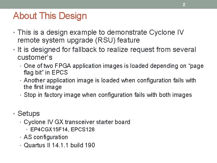
2 About This Design • This is a design example to demonstrate Cyclone IV remote system upgrade (RSU) feature • It is designed for fallback to realize request from several customer’s • One of two FPGA application images is loaded depending on “page flag bit” in EPCS • Another application image is loaded when configuration fails with the first image • Stop in factory image when configuration fails with both images • Setups • Cyclone IV GX transceiver starter board • EP 4 CGX 15 F 14, EPCS 128 • AS configuration • Quartus II 14. 1. 1 build 190

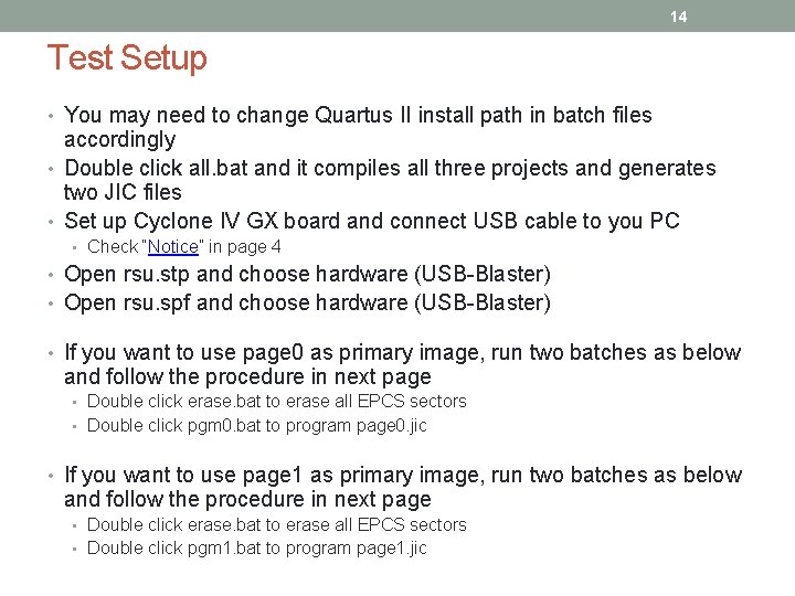
3 Reference Documents • Cyclone IV Handbook • https: //www. altera. com/content/dam/alterawww/global/en_US/pdfs/literature/hb/cyclone-iv/cyiv-5 v 1. pdf • Altera Remote Update IP Core User Guide • https: //www. altera. com/content/dam/alterawww/global/en_US/pdfs/literature/ug/ug_altremote. pdf • Altera ASMI Parallel IP Core User Guide • https: //www. altera. com/content/dam/alterawww/global/en_US/pdfs/literature/ug/ug_altasmi_parallel. pdf • Cyclone IV GX Transceiver Starter Kit User Guide • https: //www. altera. com/content/dam/alterawww/global/en_US/pdfs/literature/ug/ug_civgx_trans_starter_kit. pdf • Cyclone IV GX Transceiver Starter Board Reference Manual • https: //www. altera. com/content/dam/alterawww/global/en_US/pdfs/literature/manual/rm_civgx_trans_starter_boar d. pdf

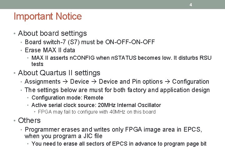
4 Important Notice • About board settings • Board switch-7 (S 7) must be ON-OFF-ON-OFF • Erase MAX II data • MAX II asserts n. CONFIG when n. STATUS becomes low. It disturbs RSU tests • About Quartus II settings • Assignments Device and Pin options Configuration • The settings below are must for both factory and application design • Configuration mode: Remote • Active serial clock source: 20 MHz Internal Oscillator • FPGA may fail to configure with 40 MHz on this board • Others • Programmer erases and writes only FPGA image area in EPCS, when you program a JIC file • You need to erase all sectors of EPCS in advance to program page bit

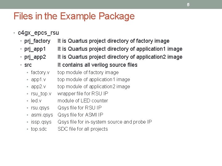
5 Files in the Example Package • c 4 gx_epcs_rsu • prj_factory • prj_app 1 • prj_app 2 • src • factory. v • app 1. v • app 2. v • rsu_top. v • led. v • rsu. qsys • asmi. qsys • issp. qsys • top. sdc It is Quartus project directory of factory image It is Quartus project directory of application 1 image It is Quartus project directory of application 2 image It contains all verilog source files top module of factory image top module of application 1 image top module of application 2 image wrapper file for RSU IP module of LED counter Qsys file for RSU IP Qsys file for ASMI IP Qsys file for in-system source and probe IP SDC file for all projects

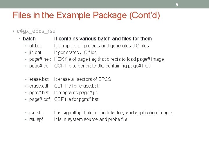
6 Files in the Example Package (Cont’d) • c 4 gx_epcs_rsu • batch • all. bat • jic. bat • page#. hex • page#. cof • erase. bat • erase. cdf • pgm#. bat • page#. cdf • rsu. stp • rsu. spf It contains various batch and files for them It compiles all projects and generates JIC files It generates JIC files HEX file of page flag that directs to load page# image COF file to generate JIC containing page#. hex It erase all sectors of EPCS CDF file for erase. bat It programs page#. jic CDF file for pgm#. bat It is signaltap II file for both factory and application images It is in-system source and probe file

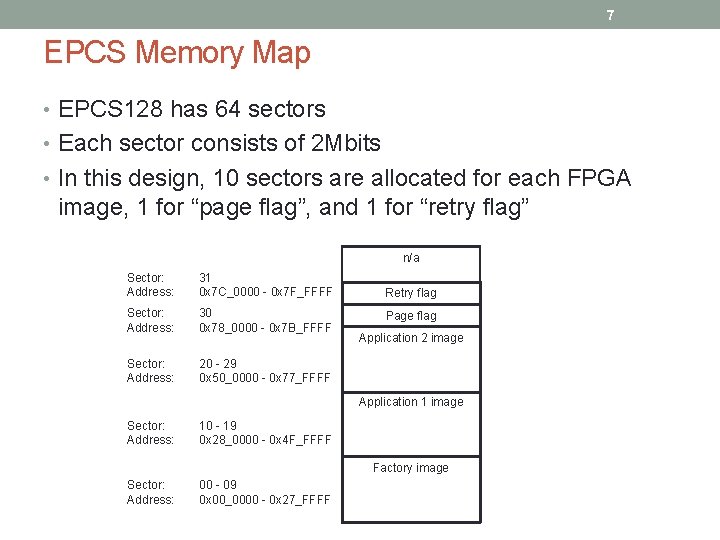
7 EPCS Memory Map • EPCS 128 has 64 sectors • Each sector consists of 2 Mbits • In this design, 10 sectors are allocated for each FPGA image, 1 for “page flag”, and 1 for “retry flag” n/a Sector: Address: 31 0 x 7 C_0000 - 0 x 7 F_FFFF Sector: Address: 30 0 x 78_0000 - 0 x 7 B_FFFF Sector: Address: 20 - 29 0 x 50_0000 - 0 x 77_FFFF Retry flag Page flag Application 2 image Application 1 image Sector: Address: 10 - 19 0 x 28_0000 - 0 x 4 F_FFFF Factory image Sector: Address: 00 - 09 0 x 00_0000 - 0 x 27_FFFF

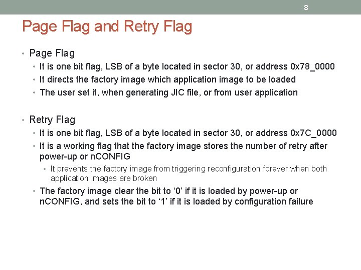
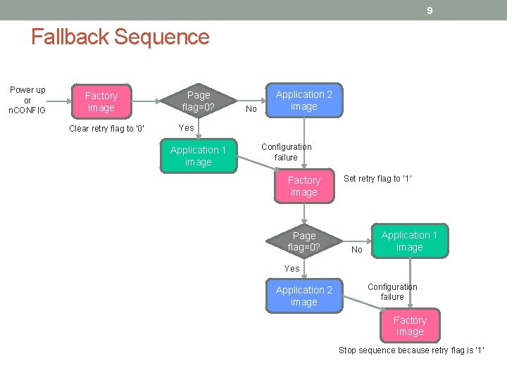
8 Page Flag and Retry Flag • Page Flag • It is one bit flag, LSB of a byte located in sector 30, or address 0 x 78_0000 • It directs the factory image which application image to be loaded • The user set it, when generating JIC file, or from user application • Retry Flag • It is one bit flag, LSB of a byte located in sector 30, or address 0 x 7 C_0000 • It is a working flag that the factory image stores the number of retry after power-up or n. CONFIG • It prevents the factory image from triggering reconfiguration forever when both application images are broken • The factory image clear the bit to ‘ 0’ if it is loaded by power-up or n. CONFIG, and sets the bit to ‘ 1’ if it is loaded by configuration failure

9 Fallback Sequence Power up or n. CONFIG Factory image Clear retry flag to ‘ 0’ Page flag=0? No Application 2 image Yes Application 1 image Configuration failure Factory image Page flag=0? Set retry flag to ‘ 1’ No Application 1 image Yes Application 2 image Configuration failure Factory image Stop sequence because retry flag is ‘ 1’

10 Block Diagram • All designs, factory, application 1, and application 2, have same structure EP 4 CGX 15 rsu_top JTAG In-System Source and Probe IP reconfig read status Altera Remote Update IP RSU FSM read write erase Main FSM check POF Altera ASMI Parallel IP EPCS read flag CLK 50 MHz Divider 1/4 12. 5 MHz led counter 4 LEDs

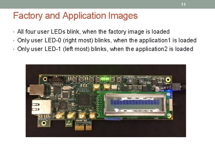
11 Factory and Application Images • All four user LEDs blink, when the factory image is loaded • Only user LED-0 (right most) blinks, when the application 1 is loaded • Only user LED-1 (left most) blinks, when the application 2 is loaded

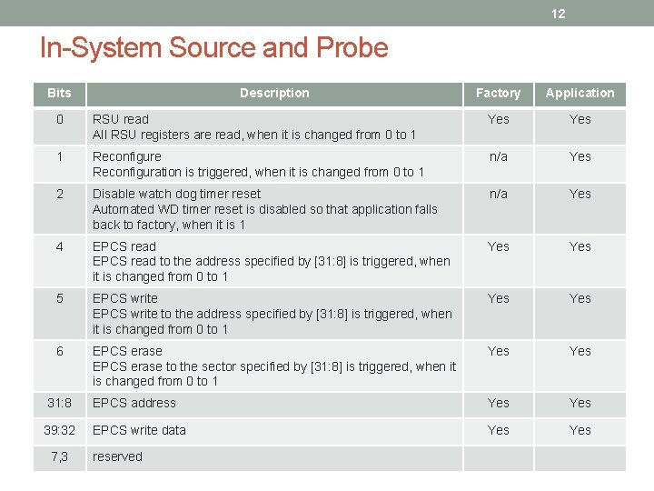
12 In-System Source and Probe Bits Description Factory Application 0 RSU read All RSU registers are read, when it is changed from 0 to 1 Yes 1 Reconfigure Reconfiguration is triggered, when it is changed from 0 to 1 n/a Yes 2 Disable watch dog timer reset Automated WD timer reset is disabled so that application falls back to factory, when it is 1 n/a Yes 4 EPCS read to the address specified by [31: 8] is triggered, when it is changed from 0 to 1 Yes 5 EPCS write to the address specified by [31: 8] is triggered, when it is changed from 0 to 1 Yes 6 EPCS erase to the sector specified by [31: 8] is triggered, when it is changed from 0 to 1 Yes 31: 8 EPCS address Yes 39: 32 EPCS write data Yes 7, 3 reserved

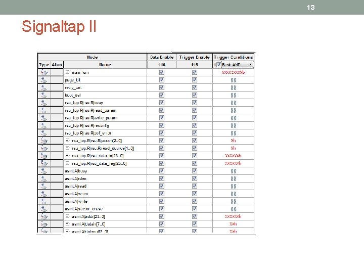
13 Signaltap II

14 Test Setup • You may need to change Quartus II install path in batch files accordingly • Double click all. bat and it compiles all three projects and generates two JIC files • Set up Cyclone IV GX board and connect USB cable to you PC • Check “Notice” in page 4 • Open rsu. stp and choose hardware (USB-Blaster) • Open rsu. spf and choose hardware (USB-Blaster) • If you want to use page 0 as primary image, run two batches as below and follow the procedure in next page • Double click erase. bat to erase all EPCS sectors • Double click pgm 0. bat to program page 0. jic • If you want to use page 1 as primary image, run two batches as below and follow the procedure in next page • Double click erase. bat to erase all EPCS sectors • Double click pgm 1. bat to program page 1. jic

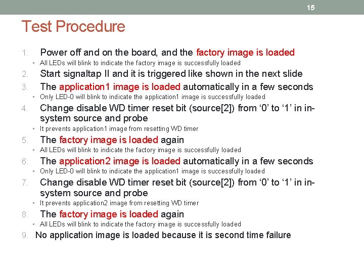
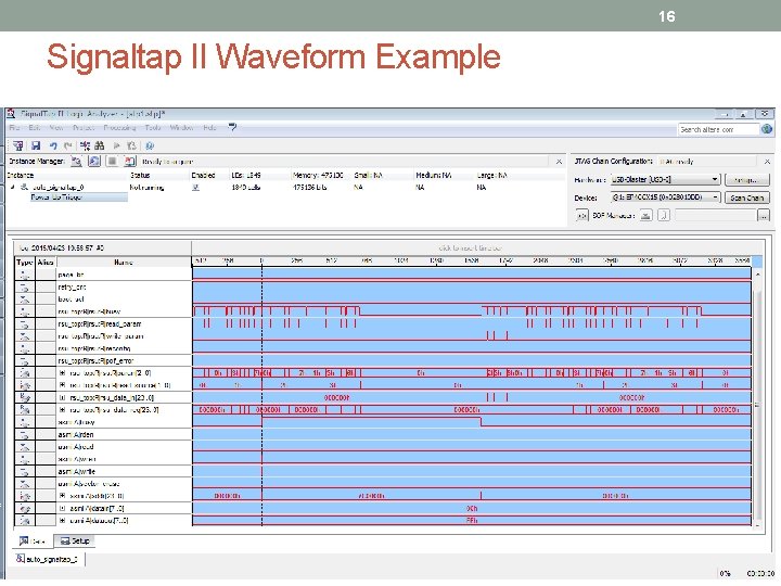
15 Test Procedure 1. Power off and on the board, and the factory image is loaded • All LEDs will blink to indicate the factory image is successfully loaded 2. 3. Start signaltap II and it is triggered like shown in the next slide The application 1 image is loaded automatically in a few seconds • Only LED-0 will blink to indicate the application 1 image is successfully loaded 4. Change disable WD timer reset bit (source[2]) from ‘ 0’ to ‘ 1’ in insystem source and probe • It prevents application 1 image from resetting WD timer 5. The factory image is loaded again • All LEDs will blink to indicate the factory image is successfully loaded 6. The application 2 image is loaded automatically in a few seconds • Only LED-0 will blink to indicate the application 1 image is successfully loaded 7. Change disable WD timer reset bit (source[2]) from ‘ 0’ to ‘ 1’ in insystem source and probe • It prevents application 2 image from resetting WD timer 8. The factory image is loaded again • All LEDs will blink to indicate the factory image is successfully loaded 9. No application image is loaded because it is second time failure

16 Signaltap II Waveform Example