Register Transfer operations 1 REGISTER TRANSFER AND MICROOPERATIONS
- Slides: 20

Register Transfer & -operations 1 REGISTER TRANSFER AND MICROOPERATIONS • Register Transfer Language • Register Transfer • Bus and Memory Transfers • Arithmetic Microoperations • Logic Microoperations • Shift Microoperations • Arithmetic Logic Shift Unit Computer Organization Computer Architectures Lab

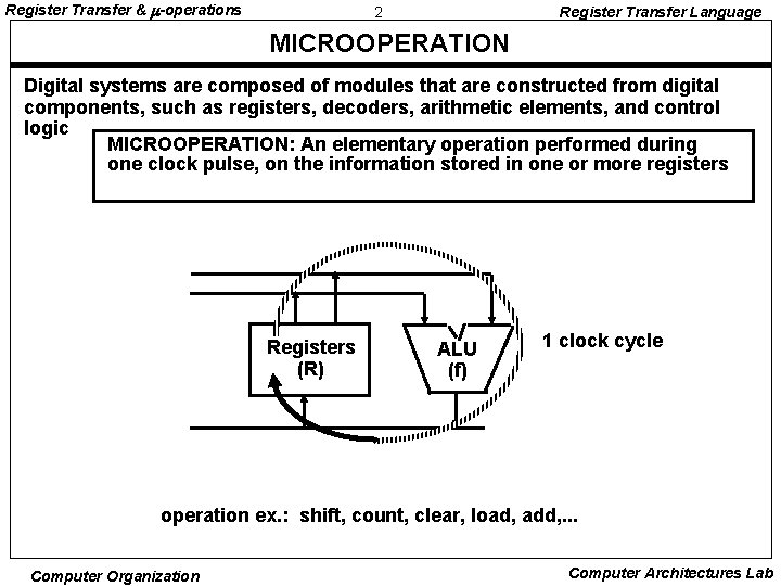
Register Transfer & -operations 2 Register Transfer Language MICROOPERATION Digital systems are composed of modules that are constructed from digital components, such as registers, decoders, arithmetic elements, and control logic MICROOPERATION: An elementary operation performed during one clock pulse, on the information stored in one or more registers Registers (R) ALU (f) 1 clock cycle operation ex. : shift, count, clear, load, add, . . . Computer Organization Computer Architectures Lab

Register Transfer & -operations 3 Register Transfer Language REGISTER TRANSFER LANGUAGE The internal hardware organization of a digital computer is best defined by specifying : • The set of registers it contains and their functions • The sequence of microoperations performed on the binary information stored • The control that initiates the sequence of microoperations For any function of the computer, a sequence of microoperations is used to describe it ----> Register transfer language - A symbolic language - A convenient tool for describing the internal organization of digital computers - Can also be used to facilitate the design process of digital systems. Computer Organization Computer Architectures Lab

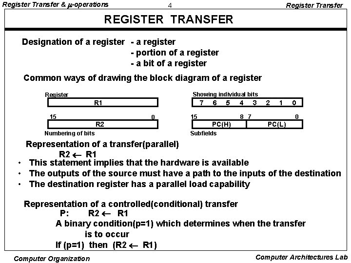
Register Transfer & -operations 4 Register Transfer REGISTER TRANSFER Designation of a register - portion of a register - a bit of a register Common ways of drawing the block diagram of a register Showing individual bits Register R 1 15 R 2 Numbering of bits 7 0 6 5 15 4 3 2 1 8 7 PC(H) 0 0 PC(L) Subfields Representation of a transfer(parallel) R 2 R 1 • This statement implies that the hardware is available • The outputs of the source must have a path to the inputs of the destination • The destination register has a parallel load capability Representation of a controlled(conditional) transfer P: R 2 R 1 A binary condition(p=1) which determines when the transfer is to occur If (p=1) then (R 2 R 1) Computer Organization Computer Architectures Lab

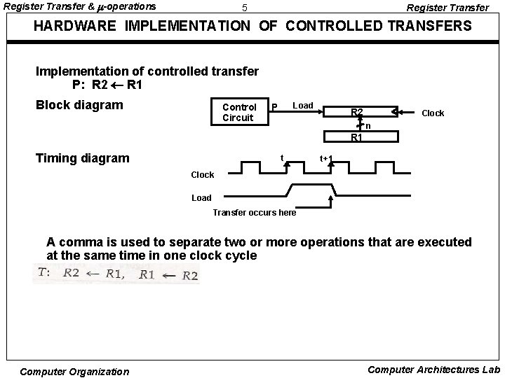
Register Transfer & -operations 5 Register Transfer HARDWARE IMPLEMENTATION OF CONTROLLED TRANSFERS Implementation of controlled transfer P: R 2 R 1 Block diagram Control Circuit Load P R 2 Clock n R 1 Timing diagram t t+1 Clock Load Transfer occurs here A comma is used to separate two or more operations that are executed at the same time in one clock cycle Computer Organization Computer Architectures Lab

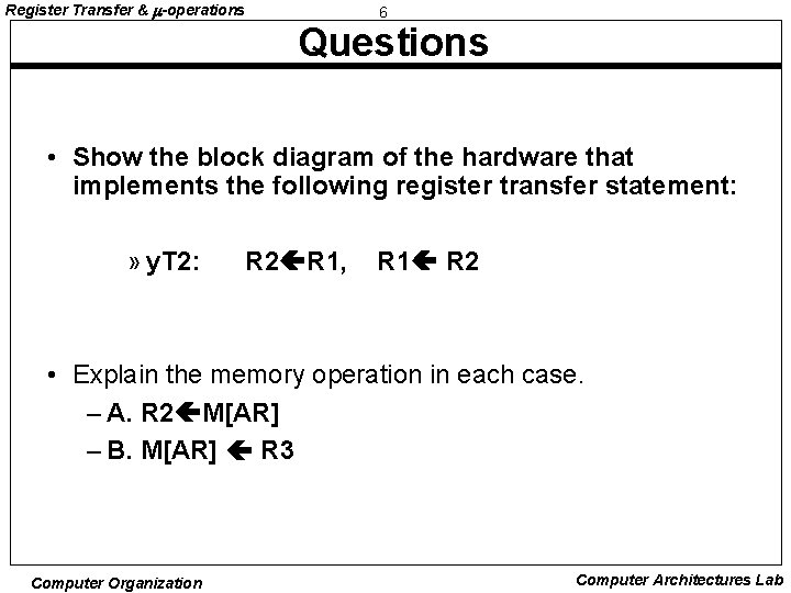
Register Transfer & -operations 6 Questions • Show the block diagram of the hardware that implements the following register transfer statement: » y. T 2: R 2 R 1, R 1 R 2 • Explain the memory operation in each case. – A. R 2 M[AR] – B. M[AR] R 3 Computer Organization Computer Architectures Lab

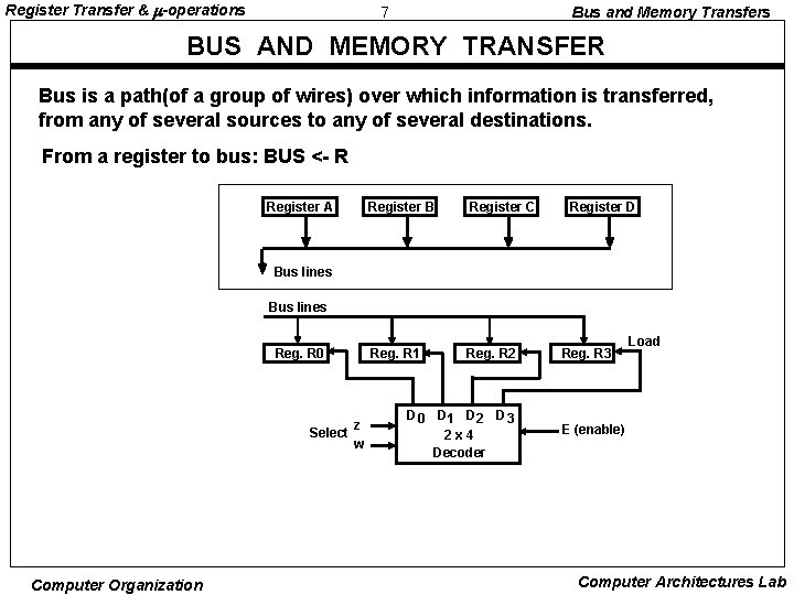
Register Transfer & -operations 7 Bus and Memory Transfers BUS AND MEMORY TRANSFER Bus is a path(of a group of wires) over which information is transferred, from any of several sources to any of several destinations. From a register to bus: BUS <- R Register A Register B Register C Reg. R 1 Reg. R 2 Register D Bus lines Reg. R 0 z Select w Computer Organization D 0 D 1 D 2 D 3 2 x 4 Decoder Reg. R 3 Load E (enable) Computer Architectures Lab

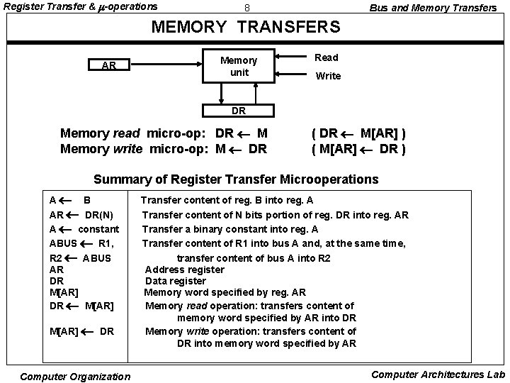
Register Transfer & -operations 8 Bus and Memory Transfers MEMORY TRANSFERS AR Memory unit Read Write DR Memory read micro-op: DR M Memory write micro-op: M DR ( DR M[AR] ) ( M[AR] DR ) Summary of Register Transfer Microoperations A B AR DR(N) A constant ABUS R 1, R 2 ABUS AR DR M[AR] DR M[AR] DR Computer Organization Transfer content of reg. B into reg. A Transfer content of N bits portion of reg. DR into reg. AR Transfer a binary constant into reg. A Transfer content of R 1 into bus A and, at the same time, transfer content of bus A into R 2 Address register Data register Memory word specified by reg. AR Memory read operation: transfers content of memory word specified by AR into DR Memory write operation: transfers content of DR into memory word specified by AR Computer Architectures Lab

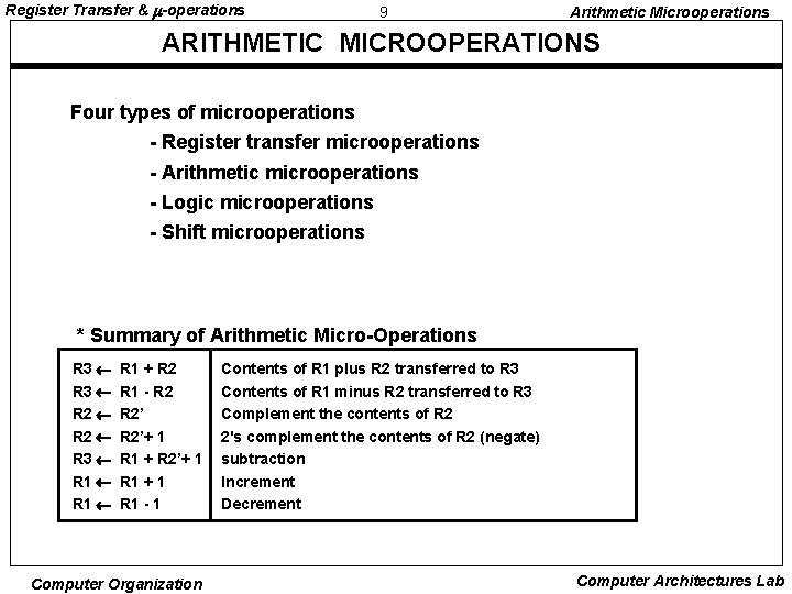
Register Transfer & -operations 9 Arithmetic Microoperations ARITHMETIC MICROOPERATIONS Four types of microoperations - Register transfer microoperations - Arithmetic microoperations - Logic microoperations - Shift microoperations * Summary of Arithmetic Micro-Operations R 3 R 1 + R 2 R 3 R 1 - R 2’ R 2’+ 1 R 3 R 1 + R 2’+ 1 R 1 - 1 Computer Organization Contents of R 1 plus R 2 transferred to R 3 Contents of R 1 minus R 2 transferred to R 3 Complement the contents of R 2 2's complement the contents of R 2 (negate) subtraction Increment Decrement Computer Architectures Lab

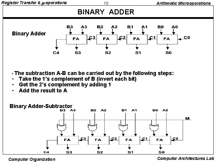
Register Transfer & -operations 10 Arithmetic Microoperations BINARY ADDER Binary Adder • The subtraction A-B can be carried out by the following steps: • Take the 1’s complement of B (invert each bit) • Get the 2’s complement by adding 1 • Add the result to A Binary Adder-Subtractor Computer Organization Computer Architectures Lab

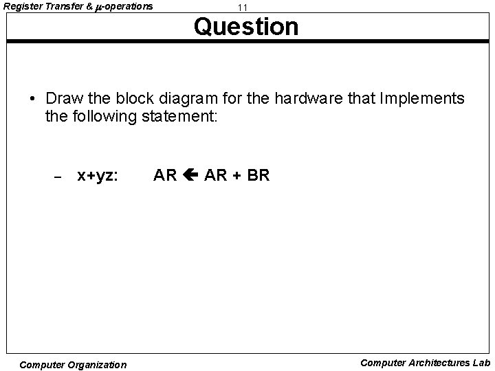
Register Transfer & -operations 11 Question • Draw the block diagram for the hardware that Implements the following statement: – x+yz: Computer Organization AR + BR Computer Architectures Lab

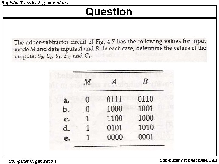
Register Transfer & -operations 12 Question Computer Organization Computer Architectures Lab

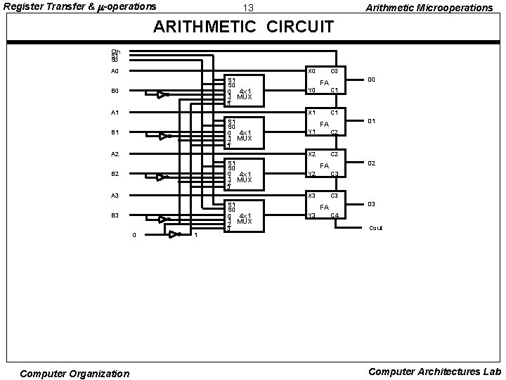
Register Transfer & -operations 13 Arithmetic Microoperations ARITHMETIC CIRCUIT Cin S 1 S 0 A 0 X 0 S 1 S 0 0 4 x 1 1 MUX 2 3 B 0 A 1 FA X 1 S 0 0 4 x 1 1 MUX 2 3 B 1 A 2 S 1 S 0 0 4 x 1 1 MUX 2 3 B 2 A 3 B 3 0 Computer Organization Y 0 C 0 1 S 0 0 4 x 1 1 MUX 2 3 D 0 C 1 D 1 FA Y 1 C 2 X 2 C 2 D 2 FA Y 2 C 3 X 3 C 3 D 3 FA Y 3 C 4 Cout Computer Architectures Lab

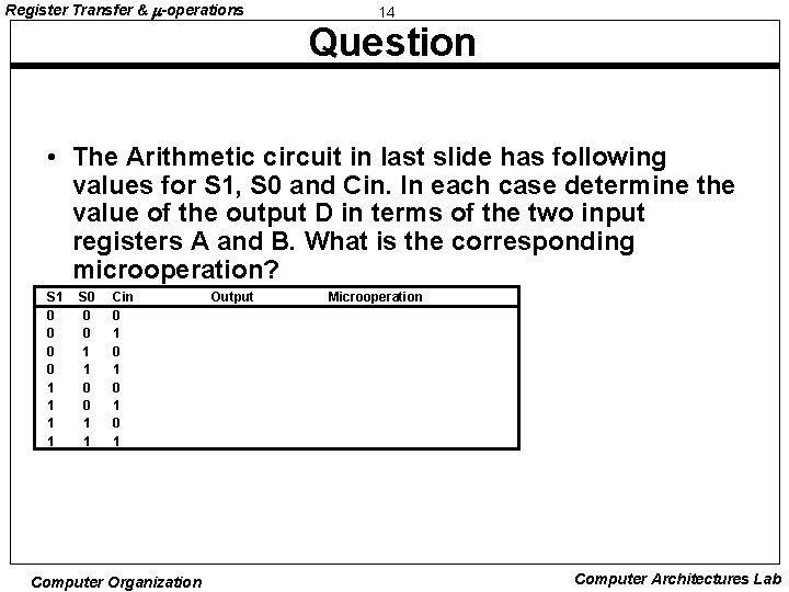
Register Transfer & -operations 14 Question • The Arithmetic circuit in last slide has following values for S 1, S 0 and Cin. In each case determine the value of the output D in terms of the two input registers A and B. What is the corresponding microoperation? S 1 0 0 1 1 S 0 0 0 1 1 Cin 0 1 0 1 Computer Organization Output Microoperation Computer Architectures Lab

Register Transfer & -operations 15 Logic Microoperations HARDWARE IMPLEMENTATION OF LOGIC MICROOPERATIONS Question: Draw the digital circuit that performs the following logical operations between reg. A and reg. B(draw the circuit for one bit), then list the circuit function table: (AND, OR, XOR and Complement). 0 Computer Organization Computer Architectures Lab

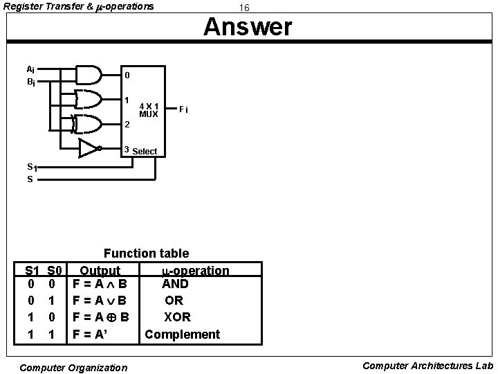
Register Transfer & -operations 16 Answer Ai Bi 0 1 4 X 1 MUX Fi 2 3 Select S 1 S Function table S 1 S 0 Output -operation 0 0 F=A B AND 0 1 F = A B OR 1 0 F=A B XOR 1 1 F = A’ Complement Computer Organization Computer Architectures Lab

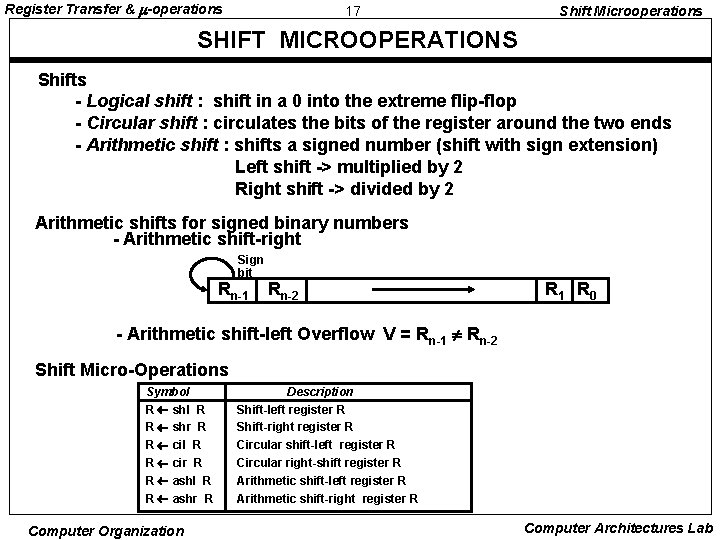
Register Transfer & -operations 17 Shift Microoperations SHIFT MICROOPERATIONS Shifts - Logical shift : shift in a 0 into the extreme flip-flop - Circular shift : circulates the bits of the register around the two ends - Arithmetic shift : shifts a signed number (shift with sign extension) Left shift -> multiplied by 2 Right shift -> divided by 2 Arithmetic shifts for signed binary numbers - Arithmetic shift-right Sign bit Rn-1 Rn-2 R 1 R 0 - Arithmetic shift-left Overflow V = Rn-1 Rn-2 Shift Micro-Operations Symbol R shl R R shr R R cil R R cir R R ashl R R ashr R Computer Organization Description Shift-left register R Shift-right register R Circular shift-left register R Circular right-shift register R Arithmetic shift-left register R Arithmetic shift-right register R Computer Architectures Lab

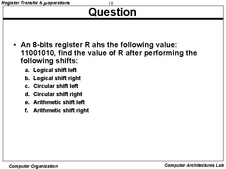
Register Transfer & -operations 18 Question • An 8 -bits register R ahs the following value: 11001010, find the value of R after performing the following shifts: a. b. c. d. e. f. Logical shift left Logical shift right Circular shift left Circular shift right Arithmetic shift left Arithmetic shift right Computer Organization Computer Architectures Lab

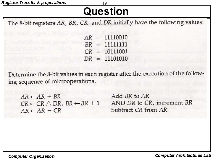
Register Transfer & -operations 19 Question Computer Organization Computer Architectures Lab

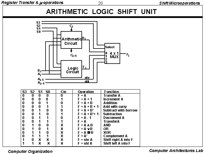
Register Transfer & -operations 20 Shift Microoperations ARITHMETIC LOGIC SHIFT UNIT S 3 S 2 S 1 S 0 Ci Arithmetic D i Circuit 0 1 2 3 Ci+1 Bi Ai Ai-1 Ai+1 S 3 0 0 0 1 1 S 2 0 0 0 0 1 1 0 1 S 0 0 0 1 0 1 0 1 1 0 0 0 1 1 X X Computer Organization Select Logic Circuit 4 x 1 MUX Fi Ei shr shl Cin 0 1 0 1 X X X Operation F=A+1 F=A+B+1 F = A + B’+ 1 F=A-1 F=A B F = A B F=A B F = A’ F = shr A F = shl A Function Transfer A Increment A Addition Add with carry Subtract with borrow Subtraction Decrement A Transfer. A AND OR XOR Complement A Shift right A into F Shift left A into F Computer Architectures Lab