Refractive index dispersion and Drude model Optics Eugene
- Slides: 15

Refractive index dispersion and Drude model Optics, Eugene Hecht, Chpt. 3

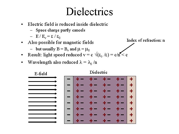
Dielectrics • Electric field is reduced inside dielectric – Space charge partly cancels – E / Ev = e / e 0 Index of refraction: n • Also possible for magnetic fields – but usually B = Bv and m = m 0 • Result: light speed reduced v = c (e 0 /e) = c/n < c • Wavelength also reduced l = l 0 /n E-field Dielectric

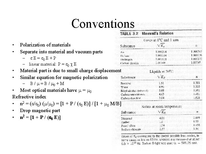
Conventions • • Polarization of materials Separate into material and vacuum parts – e E = e 0 E + P – linear material: P = e 0 c E • • Material part is due to small charge displacement Similar equation for magnetic polarization – B / m = B / m 0 + M • Most optical materials have m = m 0 Refractive index • n 2 = (e/e 0) (m/m 0) = [1 + P / (e 0 E)] / [1 + m 0 M/B] • Drop magnetic part • n 2 = [1 + P / (e 0 E)]

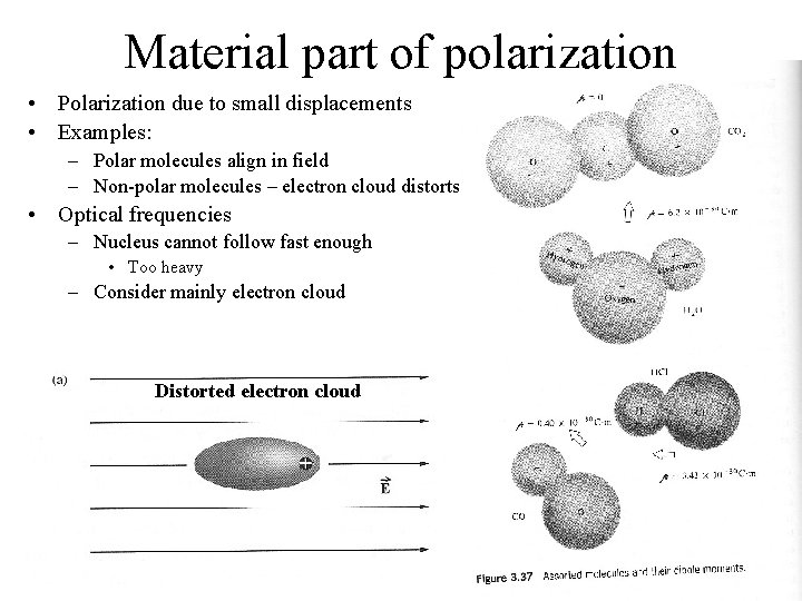
Material part of polarization • Polarization due to small displacements • Examples: – Polar molecules align in field – Non-polar molecules – electron cloud distorts • Optical frequencies – Nucleus cannot follow fast enough • Too heavy – Consider mainly electron cloud Distorted electron cloud

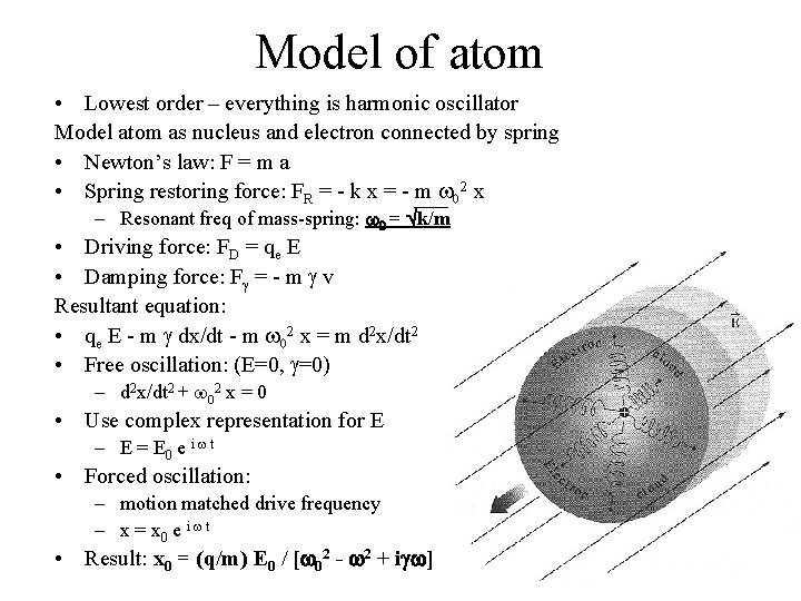
Model of atom • Lowest order – everything is harmonic oscillator Model atom as nucleus and electron connected by spring • Newton’s law: F = m a • Spring restoring force: FR = - k x = - m w 02 x – Resonant freq of mass-spring: w 0 = k/m • Driving force: FD = qe E • Damping force: Fg = - m g v Resultant equation: • qe E - m g dx/dt - m w 02 x = m d 2 x/dt 2 • Free oscillation: (E=0, g=0) – d 2 x/dt 2 + w 02 x = 0 • Use complex representation for E – E = E 0 e i w t • Forced oscillation: – motion matched drive frequency – x = x 0 e i w t • Result: x 0 = (q/m) E 0 / [w 02 - w 2 + igw]

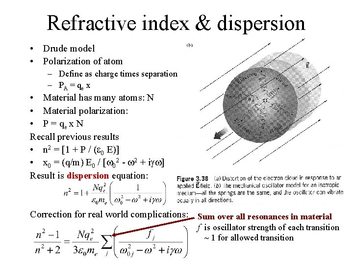
Refractive index & dispersion • Drude model • Polarization of atom – Define as charge times separation – PA = qe x • Material has many atoms: N • Material polarization: • P = qe x N Recall previous results • n 2 = [1 + P / (e 0 E)] • x 0 = (q/m) E 0 / [w 02 - w 2 + igw] Result is dispersion equation: Correction for real world complications: Sum over all resonances in material f is oscillator strength of each transition ~ 1 for allowed transition

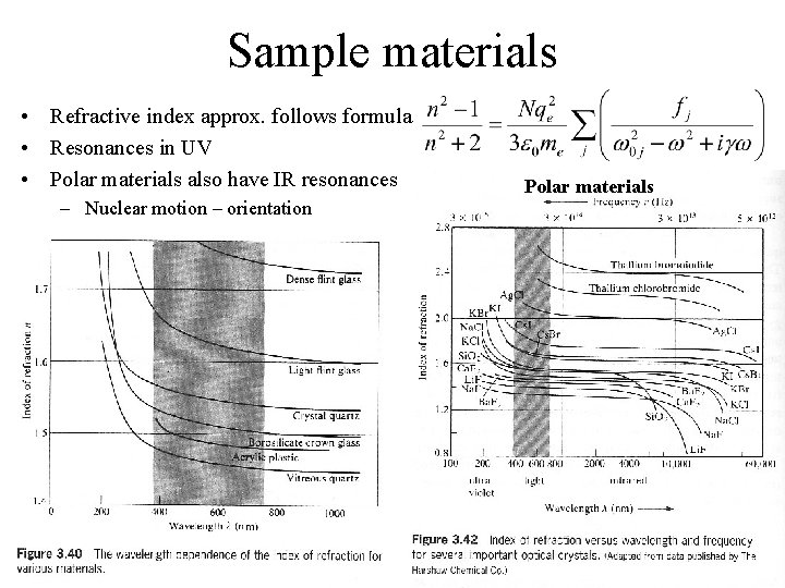
Sample materials • Refractive index approx. follows formula • Resonances in UV • Polar materials also have IR resonances – Nuclear motion – orientation Polar materials

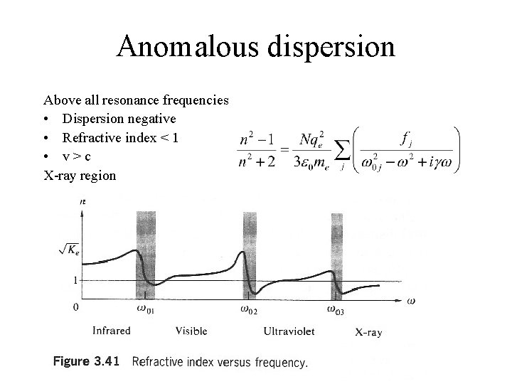
Anomalous dispersion Above all resonance frequencies • Dispersion negative • Refractive index < 1 • v>c X-ray region

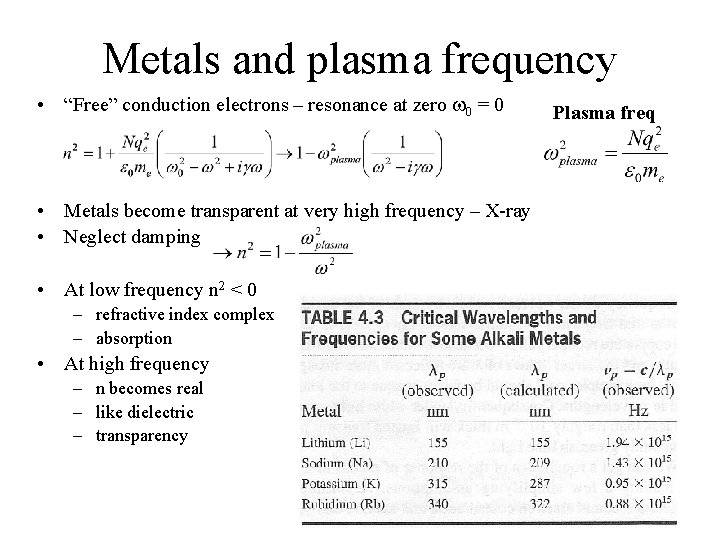
Metals and plasma frequency • “Free” conduction electrons – resonance at zero w 0 = 0 • Metals become transparent at very high frequency – X-ray • Neglect damping • At low frequency n 2 < 0 – refractive index complex – absorption • At high frequency – n becomes real – like dielectric – transparency Plasma freq

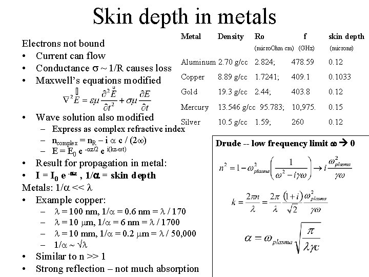
Skin depth in metals Electrons not bound • Current can flow • Conductance s ~ 1/R causes loss • Maxwell’s equations modified • Wave solution also modified Metal Ro f (micro. Ohm cm) (GHz) skin depth (microns) Aluminum 2. 70 g/cc 2. 824; 478. 59 0. 12 Copper 8. 89 g/cc 1. 7241; 409. 1 0. 1033 Gold 19. 3 g/cc 2. 44; 403. 8 0. 12 Mercury 13. 546 g/cc 95. 783; 10, 975. 0. 15 Silver 10. 5 g/cc 1. 59; 0. 12 – Express as complex refractive index – ncomplex = n. R – i a c / (2 w) – E = E 0 e -az/2 e i(kz-wt) • Result for propagation in metal: • I = I 0 e -az , 1/a = skin depth Metals: 1/a << l • Example copper: – – Density l = 100 nm, 1/a = 0. 6 nm = l / 170 l = 10 mm, 1/a = 6 nm = l / 1700 l = 10 mm, 1/a = 0. 2 mm = l / 50, 000 1/a ~ l • Similar to n >> 1 • Strong reflection – not much absorption 260 Drude -- low frequency limit w 0

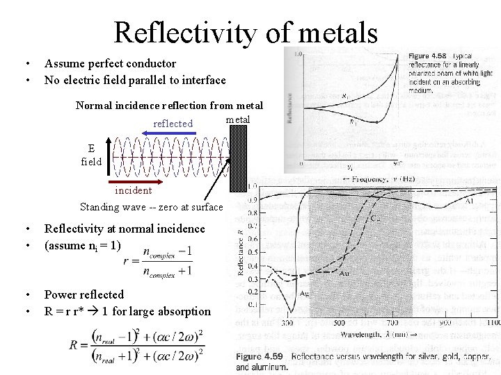
Reflectivity of metals • • Assume perfect conductor No electric field parallel to interface Normal incidence reflection from metal reflected E field incident Standing wave -- zero at surface • • Reflectivity at normal incidence (assume ni = 1) • • Power reflected R = r r* 1 for large absorption

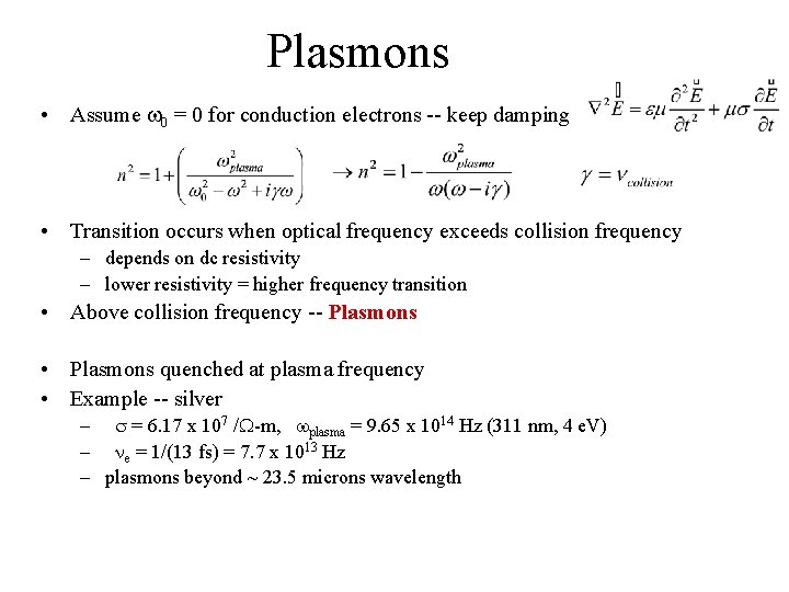
Plasmons • Assume w 0 = 0 for conduction electrons -- keep damping • Transition occurs when optical frequency exceeds collision frequency – depends on dc resistivity – lower resistivity = higher frequency transition • Above collision frequency -- Plasmons • Plasmons quenched at plasma frequency • Example -- silver – s = 6. 17 x 107 /W-m, wplasma = 9. 65 x 1014 Hz (311 nm, 4 e. V) – ne = 1/(13 fs) = 7. 7 x 10¹³ Hz – plasmons beyond ~ 23. 5 microns wavelength

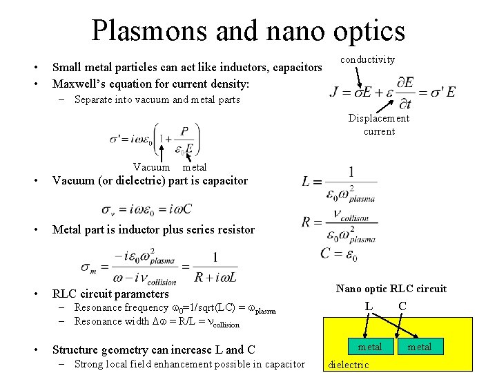
Plasmons and nano optics • • Small metal particles can act like inductors, capacitors Maxwell’s equation for current density: conductivity – Separate into vacuum and metal parts Displacement current Vacuum metal • Vacuum (or dielectric) part is capacitor • Metal part is inductor plus series resistor • RLC circuit parameters • Structure geometry can increase L and C – Resonance frequency w 0=1/sqrt(LC) = wplasma – Resonance width Dw = R/L = ncollision – Strong local field enhancement possible in capacitor Nano optic RLC circuit L metal dielectric C metal

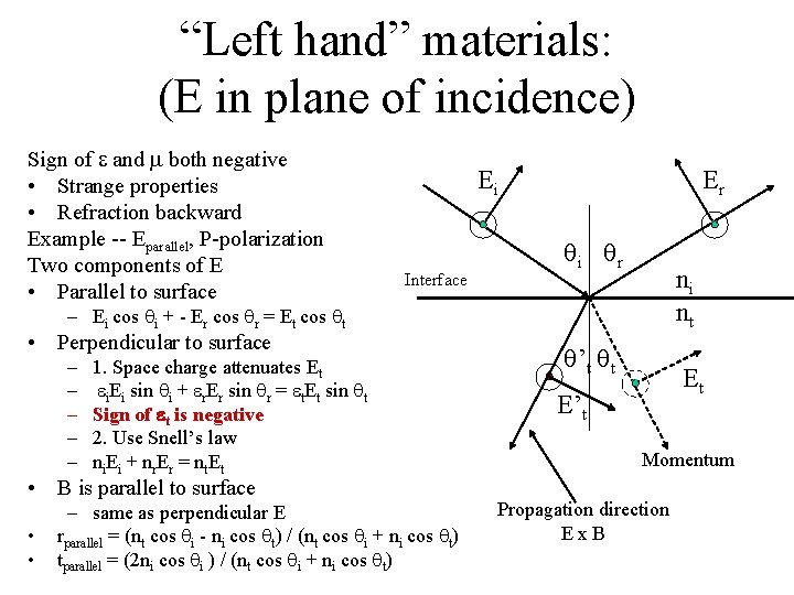
“Left hand” materials: (E in plane of incidence) Sign of e and m both negative • Strange properties • Refraction backward Example -- Eparallel, P-polarization Two components of E • Parallel to surface Ei Interface Er qi qr ni nt – Ei cos qi + - Er cos qr = Et cos qt • Perpendicular to surface – – – 1. Space charge attenuates Et ei. Ei sin qi + er. Er sin qr = et. Et sin qt Sign of et is negative 2. Use Snell’s law ni. Ei + nr. Er = nt. Et • B is parallel to surface • • – same as perpendicular E rparallel = (nt cos qi - ni cos qt) / (nt cos qi + ni cos qt) tparallel = (2 ni cos qi ) / (nt cos qi + ni cos qt) q’t qt Et E’t Momentum Propagation direction Ex. B

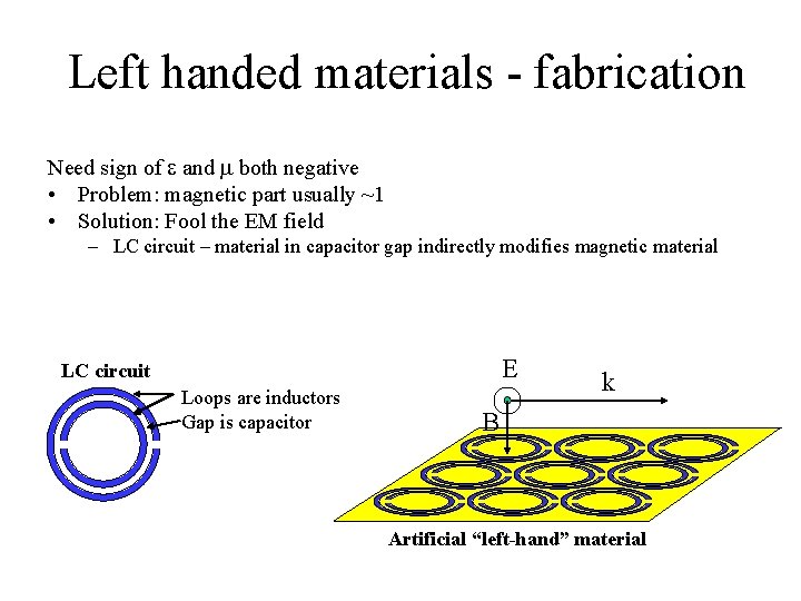
Left handed materials - fabrication Need sign of e and m both negative • Problem: magnetic part usually ~1 • Solution: Fool the EM field – LC circuit – material in capacitor gap indirectly modifies magnetic material E LC circuit Loops are inductors Gap is capacitor k B Artificial “left-hand” material