
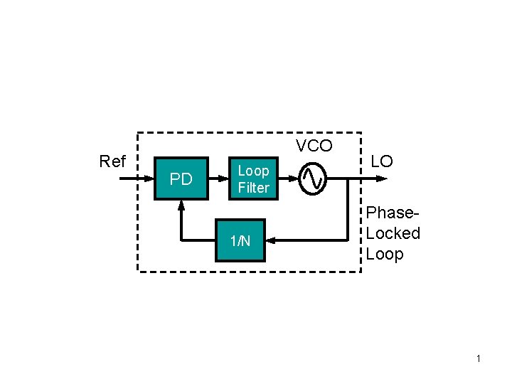
Ref VCO PD Loop Filter 1N LO Phase
- Slides: 25
Ref VCO PD Loop Filter 1/N LO Phase. Locked Loop 1
Frequency Divider Design Example Yu Lin 2
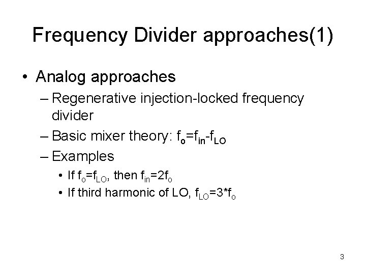
Frequency Divider approaches(1) • Analog approaches – Regenerative injection-locked frequency divider – Basic mixer theory: fo=fin-f. LO – Examples • If fo=f. LO, then fin=2 fo • If third harmonic of LO, f. LO=3*fo 3
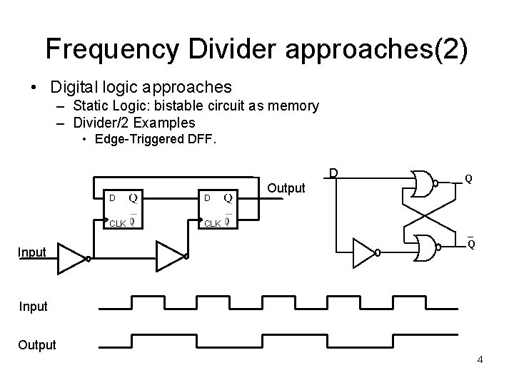
Frequency Divider approaches(2) • Digital logic approaches – Static Logic: bistable circuit as memory – Divider/2 Examples • Edge-Triggered DFF. D Input D D CLK Output Q Q Input Output 4
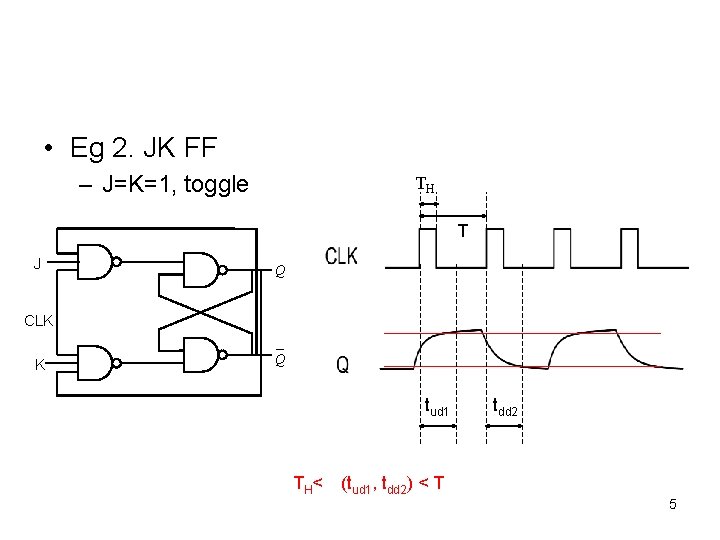
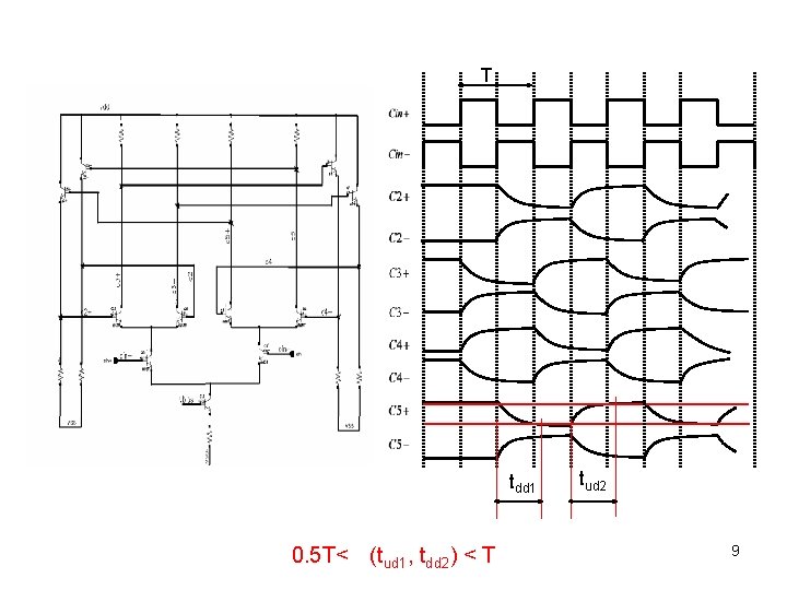
• Eg 2. JK FF – J=K=1, toggle TH T J Q CLK K Q tud 1 tdd 2 TH< (tud 1, tdd 2) < T 5
Frequency Divider approaches(3) • Digital logic approaches – – Dynamic Logic No dedicated bistable circuit Parasitic cap between node as storage element Compared to static approach • • • Faster Simpler implementation Frequency has lower limit 6
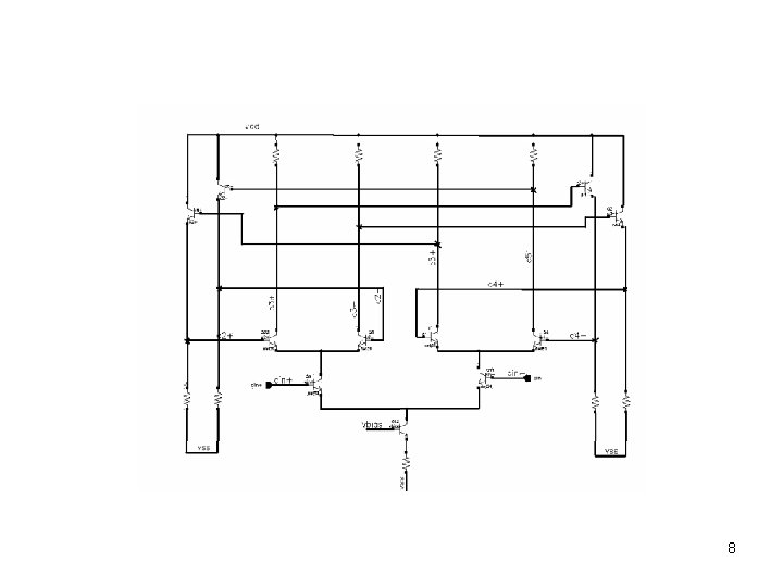
Design of divide/2 – – – – Si. Ge Bi. CMOS Dynamic frequency divider Input frequency: 40 GHz +/-20% input frequency range (32 GHz~48 GHz) Work from 0 C to 100 C at 40 GHz Input 200 mv Output 200 m. V Reinhold, M. ; Dorschky, C. ; Rose, E. ; Pullela, R. ; Mayer, P. ; Kunz, F. ; Baeyens, Y. ; Link, T. ; Mattia, J. -P. , A fully integrated 40 -Gb/s clock and data recovery IC with 1: 4 DEMUX in Si. Ge technology, Solid-State Circuits, IEEE Journal of Vol. 36, Issue 12, Dec. 2001 Page(s): 1937 - 1945 7
8
T tdd 1 0. 5 T< (tud 1, tdd 2) < T tud 2 9
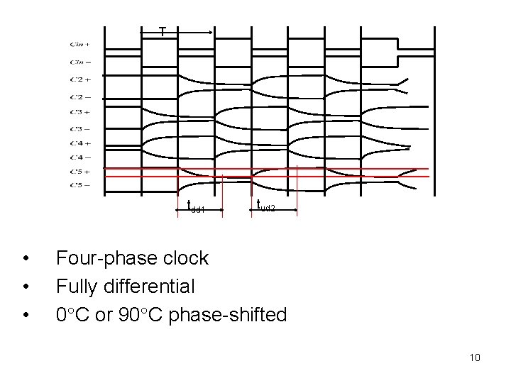
T tdd 1 • • • tud 2 Four-phase clock Fully differential 0 C or 90 C phase-shifted 10
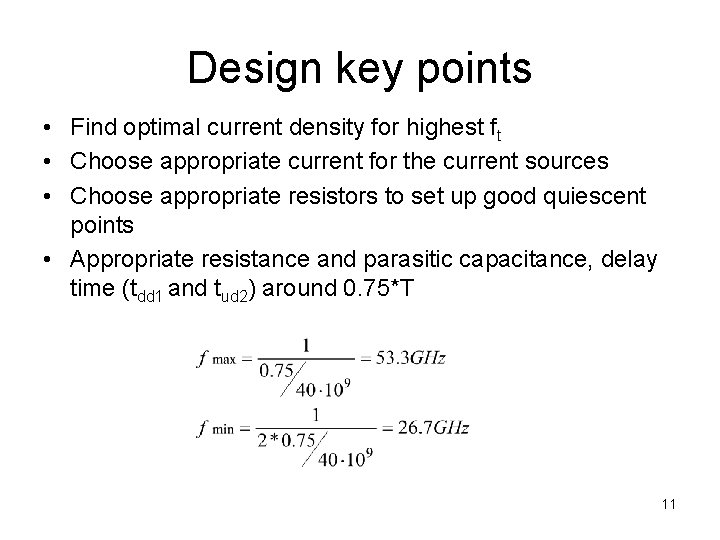
Design key points • Find optimal current density for highest ft • Choose appropriate current for the current sources • Choose appropriate resistors to set up good quiescent points • Appropriate resistance and parasitic capacitance, delay time (tdd 1 and tud 2) around 0. 75*T 11
Design key points(2) • Resistances are related to the quiescent point and input frequency range, key point of robust design • Added buffer to do level shifting, improve the driving capability and adjust gain • Driving capability increases when increase the current 12
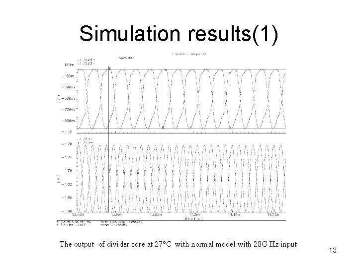
Simulation results(1) The output of divider core at 27°C with normal model with 28 G Hz input 13
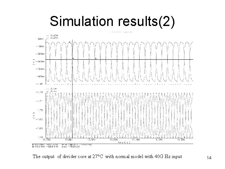
Simulation results(2) The output of divider core at 27°C with normal model with 40 G Hz input 14
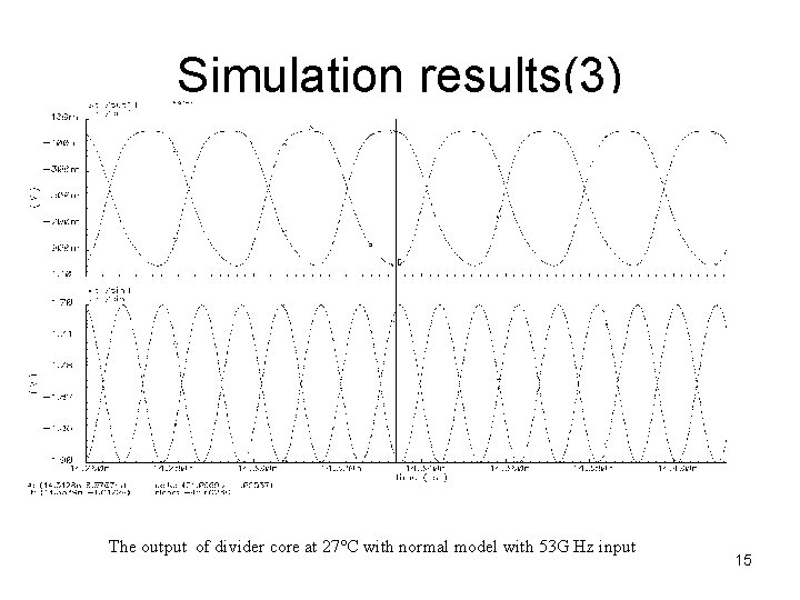
Simulation results(3) The output of divider core at 27°C with normal model with 53 G Hz input 15
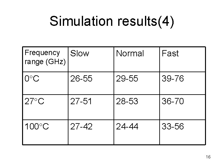
Simulation results(4) Frequency Slow range (GHz) Normal Fast 0 C 26 -55 29 -55 39 -76 27 C 27 -51 28 -53 36 -70 100 C 27 -42 24 -44 33 -56 16
VCO Design Example Chao Su; Thoka, S. ; Kee-Chee Tiew; Geiger, R. L. , A 40 GHz modified-Colpitts voltage controlled oscillator with increased tuning range, ISCAS '03. Proceedings of the 2003 International Symposium on. Volume 1, 25 -28 May 2003 Page(s): I-717 - I-720 vol. 1 17
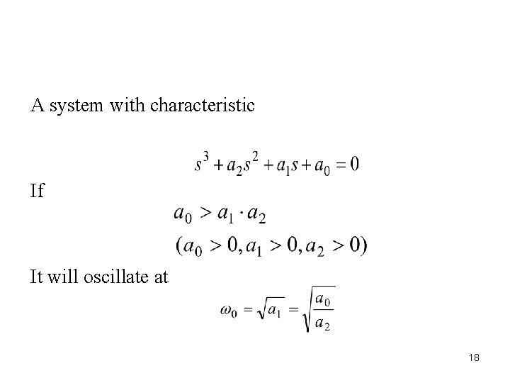
A system with characteristic If It will oscillate at 18
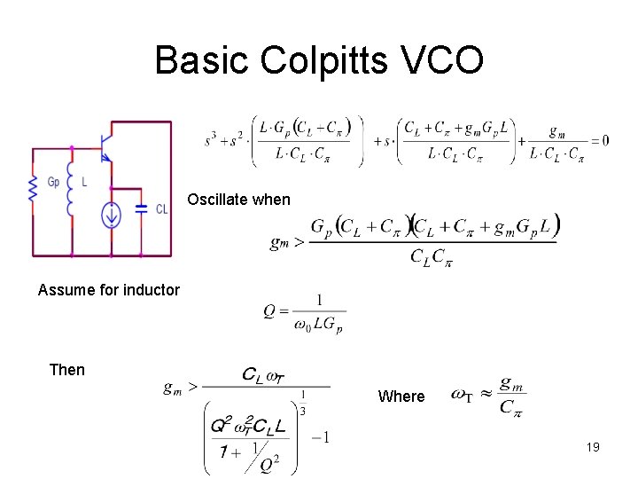
Basic Colpitts VCO Oscillate when Assume for inductor Then Where 19
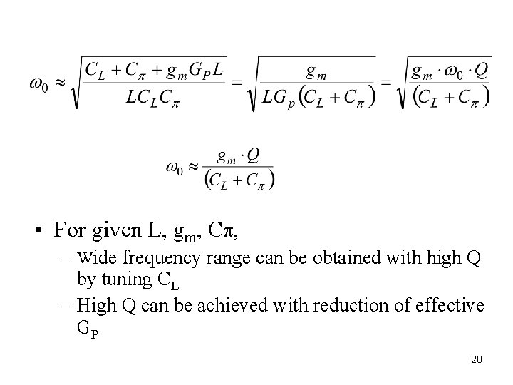
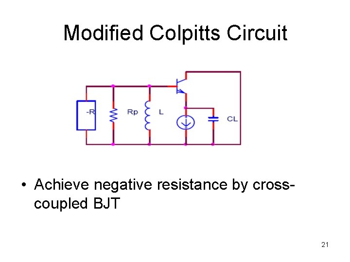
• For given L, gm, C , – Wide frequency range can be obtained with high Q by tuning CL – High Q can be achieved with reduction of effective GP 20
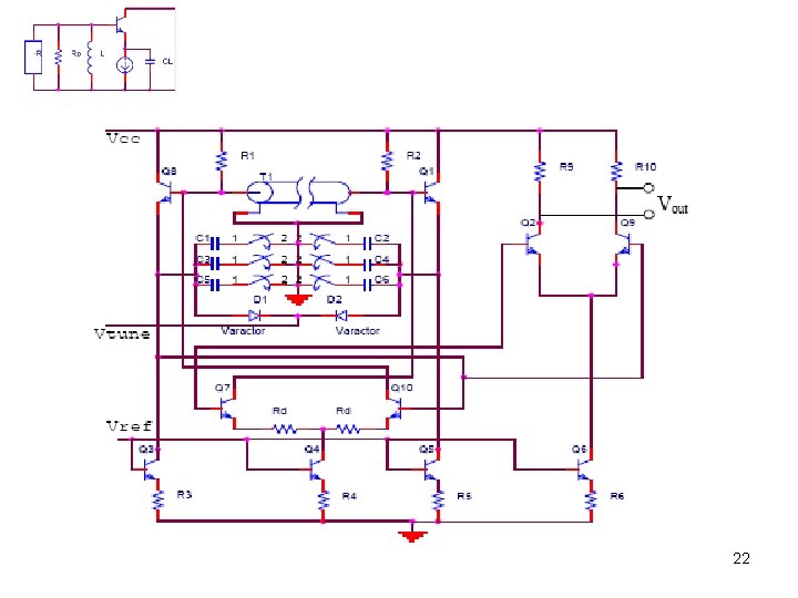
Modified Colpitts Circuit • Achieve negative resistance by crosscoupled BJT 21
22
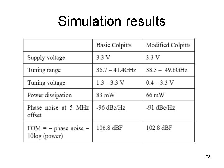
Simulation results 23
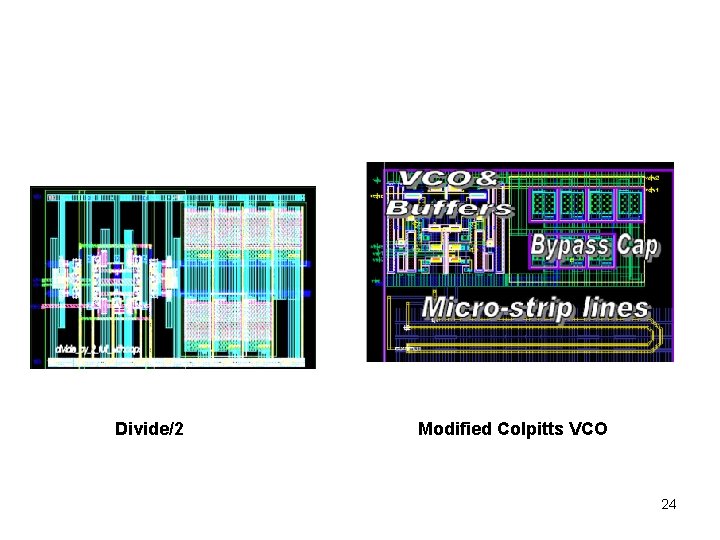
Divide/2 Modified Colpitts VCO 24
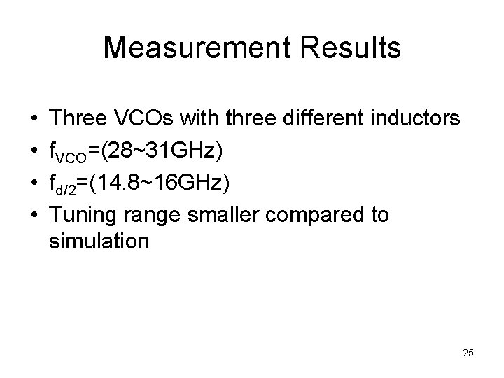
Measurement Results • • Three VCOs with three different inductors f. VCO=(28~31 GHz) fd/2=(14. 8~16 GHz) Tuning range smaller compared to simulation 25