RECIPES FOR PLASMA ATOMIC LAYER ETCHING Ankur Agarwala
- Slides: 19

RECIPES FOR PLASMA ATOMIC LAYER ETCHING* Ankur Agarwala) and Mark J. Kushnerb) a)Department of Chemical and Biomolecular Engineering University of Illinois, Urbana, IL 61801, USA aagarwl 3@uiuc. edu b)Department of Electrical and Computer Engineering Iowa State University, Ames, IA 50011, USA mjk@iastate. edu http: //uigelz. ece. iastate. edu 34 th IEEE ICOPS, June 2007 *Work supported by the SRC and NSF

AGENDA · Atomic Layer Processing · Plasma Atomic Layer Etching (PALE) · Non-sinusoidal Bias Waveforms · Tailored Bias PALE Recipes · Si. O 2 using Ar/c-C 4 F 8 · Self-aligned contacts · Concluding Remarks ANKUR_ICOPS 07_Agenda Iowa State University Optical and Discharge Physics

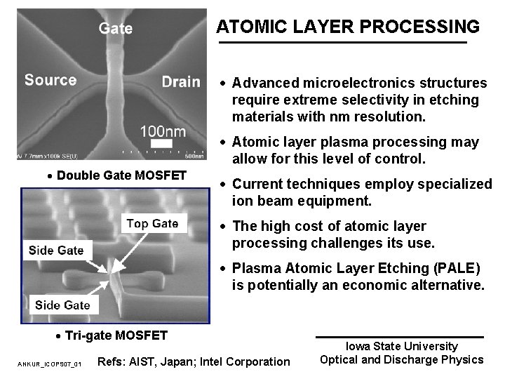
ATOMIC LAYER PROCESSING · Advanced microelectronics structures require extreme selectivity in etching materials with nm resolution. · Atomic layer plasma processing may allow for this level of control. · Double Gate MOSFET · Current techniques employ specialized ion beam equipment. · The high cost of atomic layer processing challenges its use. · Plasma Atomic Layer Etching (PALE) is potentially an economic alternative. · Tri-gate MOSFET ANKUR_ICOPS 07_01 Refs: AIST, Japan; Intel Corporation Iowa State University Optical and Discharge Physics

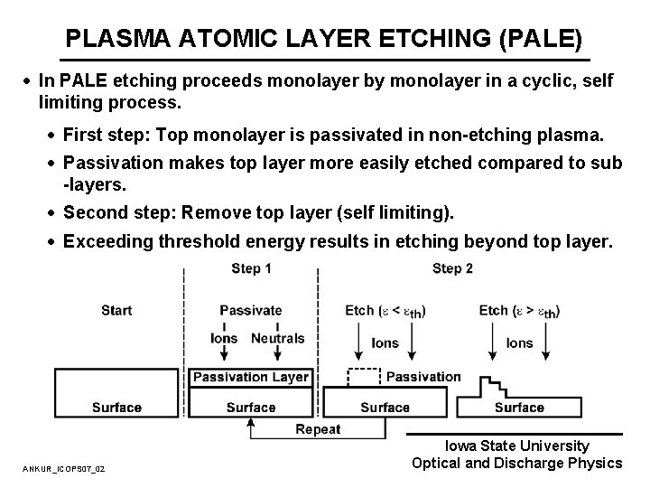
PLASMA ATOMIC LAYER ETCHING (PALE) · In PALE etching proceeds monolayer by monolayer in a cyclic, self limiting process. · First step: Top monolayer is passivated in non-etching plasma. · Passivation makes top layer more easily etched compared to sub -layers. · Second step: Remove top layer (self limiting). · Exceeding threshold energy results in etching beyond top layer. ANKUR_ICOPS 07_02 Iowa State University Optical and Discharge Physics

PLASMA ATOMIC LAYER ETCHING (PALE) · PALE has been computationally and experimentally investigated using conventional plasma equipment. · Inductively coupled plasma (ICP) · Capacitively coupled plasma (CCP) · Since the equipment is already in fabrication facilities, no additional integration costs are incurred. · The low speed of PALE processes hinder its integration into production line. · Speed can be increased but only at the cost of losing control of CD (critical dimensions) or damaging material interfaces. ANKUR_ICOPS 07_03 Iowa State University Optical and Discharge Physics

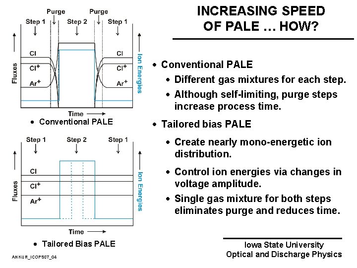
INCREASING SPEED OF PALE … HOW? · Conventional PALE · Different gas mixtures for each step. · Although self-limiting, purge steps increase process time. · Conventional PALE · Tailored bias PALE · Create nearly mono-energetic ion distribution. · Control ion energies via changes in voltage amplitude. · Single gas mixture for both steps eliminates purge and reduces time. · Tailored Bias PALE ANKUR_ICOPS 07_04 Iowa State University Optical and Discharge Physics

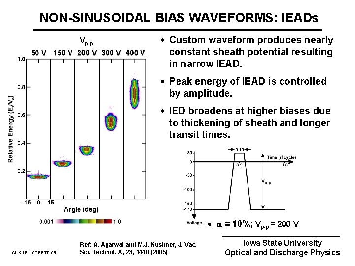
NON-SINUSOIDAL BIAS WAVEFORMS: IEADs Vp-p · Custom waveform produces nearly constant sheath potential resulting in narrow IEAD. · Peak energy of IEAD is controlled by amplitude. · IED broadens at higher biases due to thickening of sheath and longer transit times. · = 10%; Vp-p = 200 V ANKUR_ICOPS 07_05 Ref: A. Agarwal and M. J. Kushner, J. Vac. Sci. Technol. A, 23, 1440 (2005) Iowa State University Optical and Discharge Physics

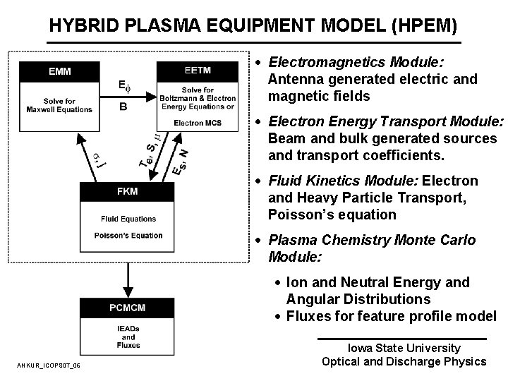
HYBRID PLASMA EQUIPMENT MODEL (HPEM) · Electromagnetics Module: Antenna generated electric and magnetic fields · Electron Energy Transport Module: Beam and bulk generated sources and transport coefficients. · Fluid Kinetics Module: Electron and Heavy Particle Transport, Poisson’s equation · Plasma Chemistry Monte Carlo Module: · Ion and Neutral Energy and Angular Distributions · Fluxes for feature profile model ANKUR_ICOPS 07_06 Iowa State University Optical and Discharge Physics

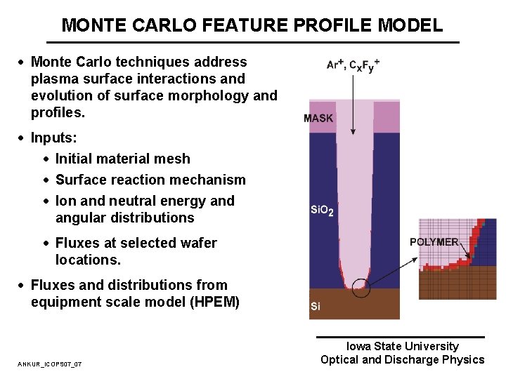
MONTE CARLO FEATURE PROFILE MODEL · Monte Carlo techniques address plasma surface interactions and evolution of surface morphology and profiles. · Inputs: · Initial material mesh · Surface reaction mechanism · Ion and neutral energy and angular distributions · Fluxes at selected wafer locations. · Fluxes and distributions from equipment scale model (HPEM) ANKUR_ICOPS 07_07 Iowa State University Optical and Discharge Physics

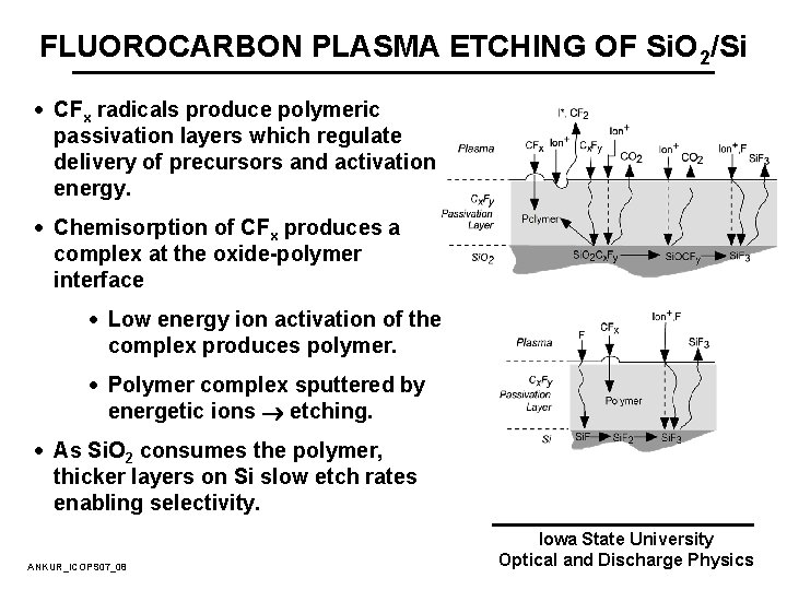
FLUOROCARBON PLASMA ETCHING OF Si. O 2/Si · CFx radicals produce polymeric passivation layers which regulate delivery of precursors and activation energy. · Chemisorption of CFx produces a complex at the oxide-polymer interface · Low energy ion activation of the complex produces polymer. · Polymer complex sputtered by energetic ions etching. · As Si. O 2 consumes the polymer, thicker layers on Si slow etch rates enabling selectivity. ANKUR_ICOPS 07_08 Iowa State University Optical and Discharge Physics

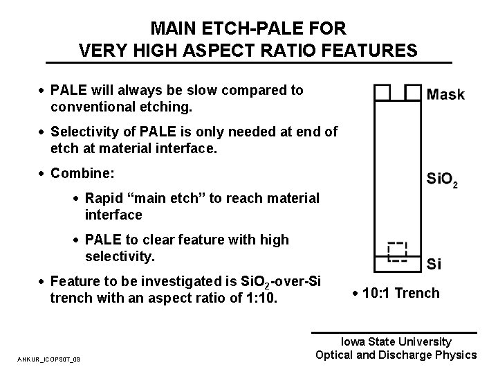
MAIN ETCH-PALE FOR VERY HIGH ASPECT RATIO FEATURES · PALE will always be slow compared to conventional etching. · Selectivity of PALE is only needed at end of etch at material interface. · Combine: · Rapid “main etch” to reach material interface · PALE to clear feature with high selectivity. · Feature to be investigated is Si. O 2 -over-Si trench with an aspect ratio of 1: 10. ANKUR_ICOPS 07_09 · 10: 1 Trench Iowa State University Optical and Discharge Physics

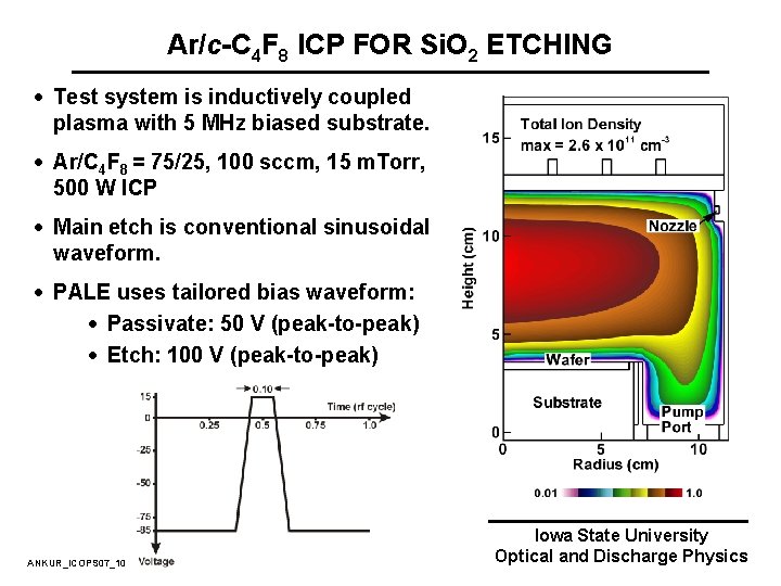
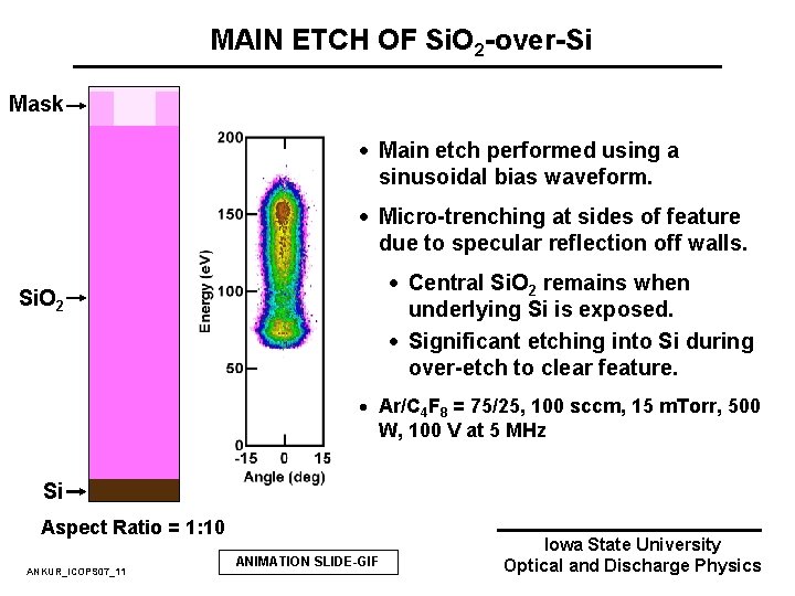
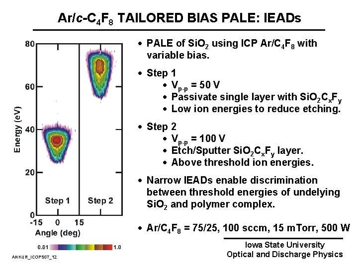
Ar/c-C 4 F 8 ICP FOR Si. O 2 ETCHING · Test system is inductively coupled plasma with 5 MHz biased substrate. · Ar/C 4 F 8 = 75/25, 100 sccm, 15 m. Torr, 500 W ICP · Main etch is conventional sinusoidal waveform. · PALE uses tailored bias waveform: · Passivate: 50 V (peak-to-peak) · Etch: 100 V (peak-to-peak) ANKUR_ICOPS 07_10 Iowa State University Optical and Discharge Physics

MAIN ETCH OF Si. O 2 -over-Si Mask · Main etch performed using a sinusoidal bias waveform. · Micro-trenching at sides of feature due to specular reflection off walls. · Central Si. O 2 remains when underlying Si is exposed. · Significant etching into Si during over-etch to clear feature. Si. O 2 · Ar/C 4 F 8 = 75/25, 100 sccm, 15 m. Torr, 500 W, 100 V at 5 MHz Si Aspect Ratio = 1: 10 ANKUR_ICOPS 07_11 ANIMATION SLIDE-GIF Iowa State University Optical and Discharge Physics

Ar/c-C 4 F 8 TAILORED BIAS PALE: IEADs · PALE of Si. O 2 using ICP Ar/C 4 F 8 with variable bias. · Step 1 · Vp-p = 50 V · Passivate single layer with Si. O 2 Cx. Fy · Low ion energies to reduce etching. · Step 2 · Vp-p = 100 V · Etch/Sputter Si. O 2 Cx. Fy layer. · Above threshold ion energies. · Narrow IEADs enable discrimination between threshold energies of undelying Si. O 2 and polymer complex. · Ar/C 4 F 8 = 75/25, 100 sccm, 15 m. Torr, 500 W ANKUR_ICOPS 07_12 Iowa State University Optical and Discharge Physics

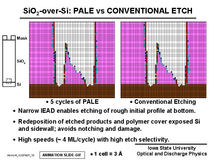
Si. O 2 -over-Si: PALE vs CONVENTIONAL ETCH Si. O 2 Si · 5 cycles of PALE · Conventional Etching · Narrow IEAD enables etching of rough initial profile at bottom. · Redeposition of etched products and polymer cover exposed Si and sidewall; avoids notching and damage. · High speeds (~ 4 ML/cycle) with high etch selectivity. ANKUR_ICOPS 07_13 ANIMATION SLIDE-GIF 1 cell = 3 Å Iowa State University Optical and Discharge Physics

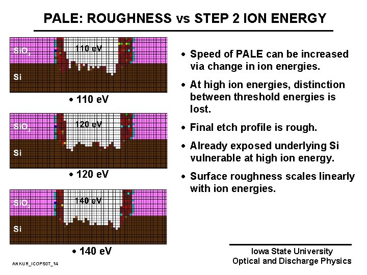
PALE: ROUGHNESS vs STEP 2 ION ENERGY · Speed of PALE can be increased via change in ion energies. · 110 e. V · At high ion energies, distinction between threshold energies is lost. · Final etch profile is rough. · Already exposed underlying Si vulnerable at high ion energy. · 120 e. V · 140 e. V ANKUR_ICOPS 07_14 · Surface roughness scales linearly with ion energies. Iowa State University Optical and Discharge Physics

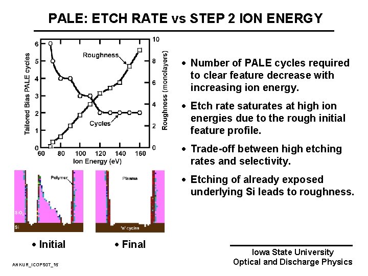
PALE: ETCH RATE vs STEP 2 ION ENERGY · Number of PALE cycles required to clear feature decrease with increasing ion energy. · Etch rate saturates at high ion energies due to the rough initial feature profile. · Trade-off between high etching rates and selectivity. · Etching of already exposed underlying Si leads to roughness. · Initial ANKUR_ICOPS 07_15 · Final Iowa State University Optical and Discharge Physics

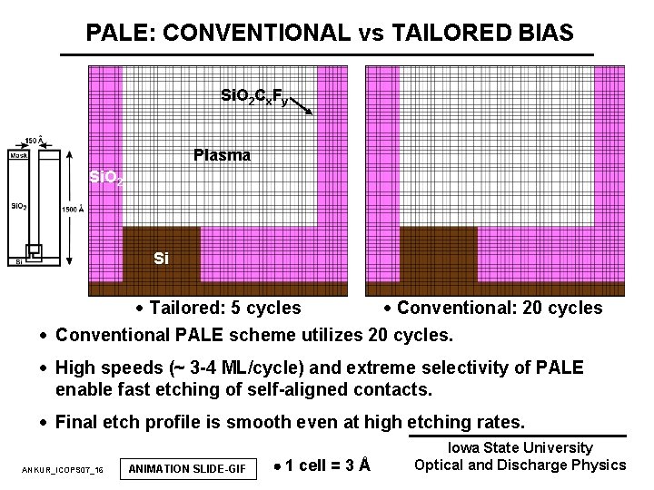
PALE: CONVENTIONAL vs TAILORED BIAS Si. O 2 Cx. Fy Plasma Si. O 2 Si · Tailored: 5 cycles · Conventional: 20 cycles · Conventional PALE scheme utilizes 20 cycles. · High speeds (~ 3 -4 ML/cycle) and extreme selectivity of PALE enable fast etching of self-aligned contacts. · Final etch profile is smooth even at high etching rates. ANKUR_ICOPS 07_16 ANIMATION SLIDE-GIF 1 cell = 3 Å Iowa State University Optical and Discharge Physics

CONCLUDING REMARKS · Atomic layer control of etch processes will be critical for 32 nm node devices. · PALE using conventional plasma equipment makes for an more economic processes. · Slow etching rates of conventional PALE need to be optimized: trade-off between high selectivity and etch rate · PALE of Si. O 2 in Ar/c-C 4 F 8 plasma investigated using custom bias waveforms, · Non-sinusoidal bias waveforms enable: · Precision control of IEADs · Elimination of purge step to increase process speeds · High selectivity at high etching rates (~ 4 ML/cycle) ANKUR_ICOPS 07_17 Iowa State University Optical and Discharge Physics