Recent developments on Monolithic Active Pixel Sensors MAPS
- Slides: 18

Recent developments on Monolithic Active Pixel Sensors (MAPS) for charged particle tracking. Michael Deveaux on behalf of IPHC Strasbourg, IKF Frankfurt/M (Irradiations: F. M. Wagner, MEDAPP, FRM II reactor Munich) Outline • The MAPS sensor (reminder) • MIMOSA-22, a fast MAPS-sensor • The SUZE-1 FEE chip • Random Telegraph Signal and radiation damage • Summary and Conclusion M. Deveaux, 12 th CBM Collaboration Meeting, 13 - 18 Oct. 2008 JINR Dubna, Russia

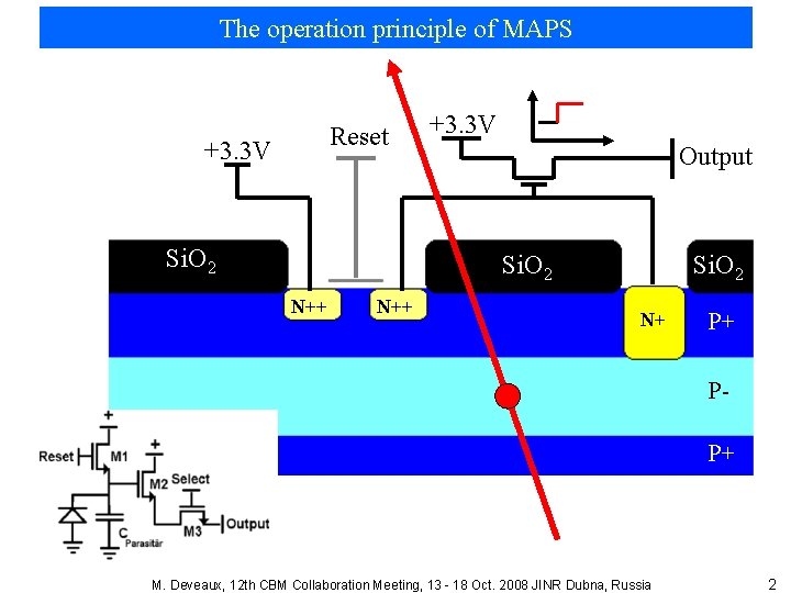
The operation principle of MAPS Reset +3. 3 V Si. O 2 +3. 3 V Output Si. O 2 N++ Si. O 2 N+ P+ PP+ M. Deveaux, 12 th CBM Collaboration Meeting, 13 - 18 Oct. 2008 JINR Dubna, Russia 2

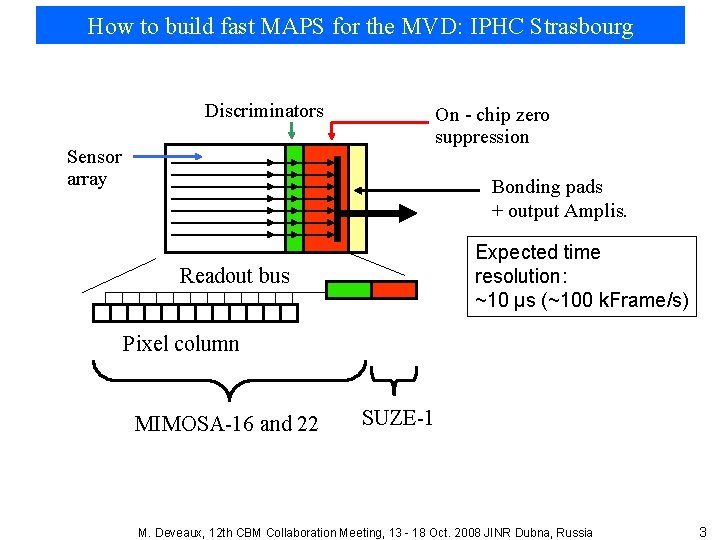
How to build fast MAPS for the MVD: IPHC Strasbourg Discriminators On - chip zero suppression Sensor array Bonding pads + output Amplis. Expected time resolution: ~10 µs (~100 k. Frame/s) Readout bus Pixel column MIMOSA-16 and 22 SUZE-1 M. Deveaux, 12 th CBM Collaboration Meeting, 13 - 18 Oct. 2008 JINR Dubna, Russia 3

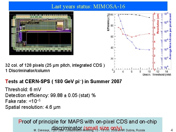
Last years status: MIMOSA-16 32 col. of 128 pixels (25 μm pitch, integrated CDS ) 1 Discriminator/column Tests at CERN-SPS ( 180 Ge. V pi−) in Summer 2007 Threshold: 6 m. V Detection efficiency: 99. 88 ± 0. 05 (stat) % Fake rate: <10− 5 Spatial resolution: 4. 6 μm Proof of principle for MAPS with on-pixel CDS and on-chip discriminator (small M. Deveaux, 12 th CBM Collaboration Meeting, 13 -size 18 Oct. only). 2008 JINR Dubna, Russia 4

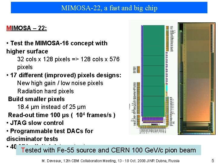
MIMOSA-22, a fast and big chip MIMOSA – 22: • Test the MIMOSA-16 concept with higher surface 32 cols x 128 pixels => 128 cols x 576 pixels • 17 different (improved) pixels designs: New high gain / low noise pixels Radiation hard pixels Build smaller pixels 18. 4 μm instead of 25 µm Read-out time 100 μs ( 104 frames/s ) • JTAG slow control • Programmable test DACs for disciminator tests • 40 MHz digital data output Tested with Fe-55 source and CERN 100 Ge. V/c pion beam M. Deveaux, 12 th CBM Collaboration Meeting, 13 - 18 Oct. 2008 JINR Dubna, Russia 5

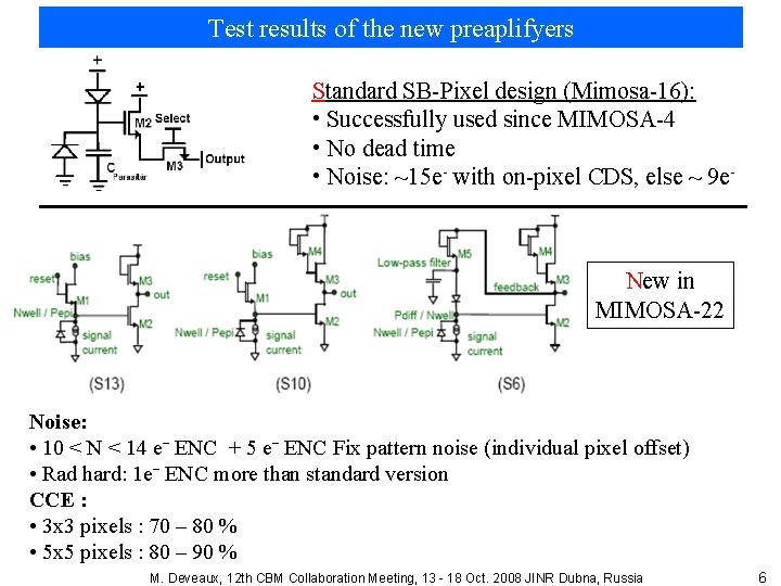
Test results of the new preaplifyers Standard SB-Pixel design (Mimosa-16): • Successfully used since MIMOSA-4 • No dead time • Noise: ~15 e- with on-pixel CDS, else ~ 9 e- New in MIMOSA-22 Noise: • 10 < N < 14 e− ENC + 5 e− ENC Fix pattern noise (individual pixel offset) • Rad hard: 1 e− ENC more than standard version CCE : • 3 x 3 pixels : 70 – 80 % • 5 x 5 pixels : 80 – 90 % M. Deveaux, 12 th CBM Collaboration Meeting, 13 - 18 Oct. 2008 JINR Dubna, Russia 6

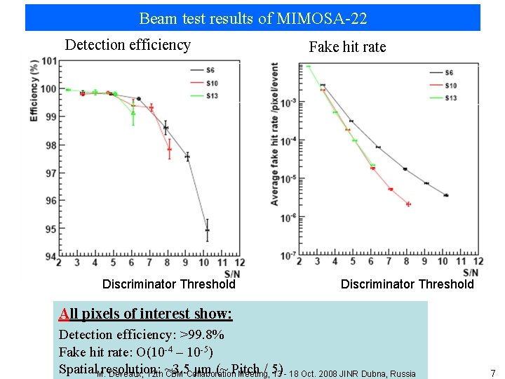
Beam test results of MIMOSA-22 Detection efficiency Discriminator Threshold Fake hit rate Discriminator Threshold All pixels of interest show: Detection efficiency: >99. 8% Fake hit rate: O(10 -4 – 10 -5) Spatial. M. resolution: µm (~ Pitch / 5) Deveaux, 12 th ~3. 5 CBM Collaboration Meeting, 13 - 18 Oct. 2008 JINR Dubna, Russia 7

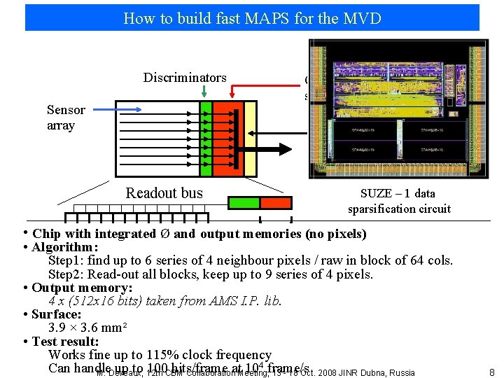
How to build fast MAPS for the MVD Discriminators Sensor array On - chip zero suppression Bonding pads + output Amplis. Readout bus SUZE – 1 data sparsification circuit • Chip with integrated Ø and output memories (no pixels) Pixel column • Algorithm: SUZE-1 Step 1: find up to 6 series of 4 neighbour pixels / raw in block of 64 cols. Step 2: Read-out all blocks, keep up to 9 series of 4 pixels. • Output memory: 4 x (512 x 16 bits) taken from AMS I. P. lib. • Surface: 3. 9 × 3. 6 mm² • Test result: Works fine up to 115% clock frequency Can handle up to 12 th 100 CBM hits/frame 104 frame/s M. Deveaux, Collaborationat Meeting, 13 - 18 Oct. 2008 JINR Dubna, Russia 8

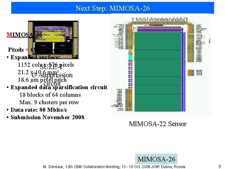
Next Step: MIMOSA-26 Pixels + Ø-suppression • Expanded surface: 1152 cols. SUZE-1 x 576 pixels 21. 2 x 10. 6 mm² Ø -suppression 18. 6 µm pixel pitch circuit • Expanded data sparsification circuit 18 blocks of 64 columns Max. 9 clusters per row • Data rate: 80 Mbits/s • Submission November 2008 MIMOSA-22 Sensor MIMOSA-26 M. Deveaux, 12 th CBM Collaboration Meeting, 13 - 18 Oct. 2008 JINR Dubna, Russia 9

Radiation hardness studies together with M. Deveaux, 12 th CBM Collaboration Meeting, 13 - 18 Oct. 2008 JINR Dubna, Russia 10

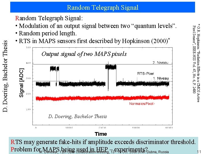
Random Telegraph Signal: • Modulation of an output signal between two “quantum levels”. • Random period length. • RTS in MAPS sensors first described by Hopkinson (2000)* Signal [ADC] Output signal of two MAPS pixels * G. R. Hopkinson: “Radiation Effects in a CMOS Active Pixel Sensor”, IEEE-NSS Vol. 47, No. 6, P. 2480 D. Doering, Bachelor Thesis Random Telegraph Signal D. Doering, Bachelor Thesis Time RTS may generate fake-hits if amplitude exceeds discriminator threshold. Problem for. M. MAPS being used in HEP Deveaux, 12 th CBM Collaboration Meeting, – 13 experiments? - 18 Oct. 2008 JINR Dubna, Russia 11

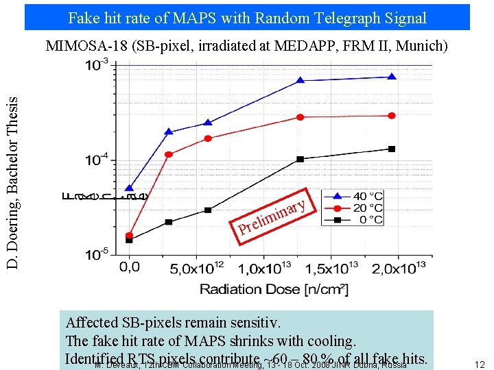
Fake hit rate of MAPS with Random Telegraph Signal D. Doering, Bachelor Thesis MIMOSA-18 (SB-pixel, irradiated at MEDAPP, FRM II, Munich) ar n i m li e r P y Affected SB-pixels remain sensitiv. The fake hit rate of MAPS shrinks with cooling. Identified RTS contribute 802008 %JINR of Dubna, all fake hits. M. Deveaux, 12 thpixels CBM Collaboration Meeting, ~60 13 - 18–Oct. Russia 12

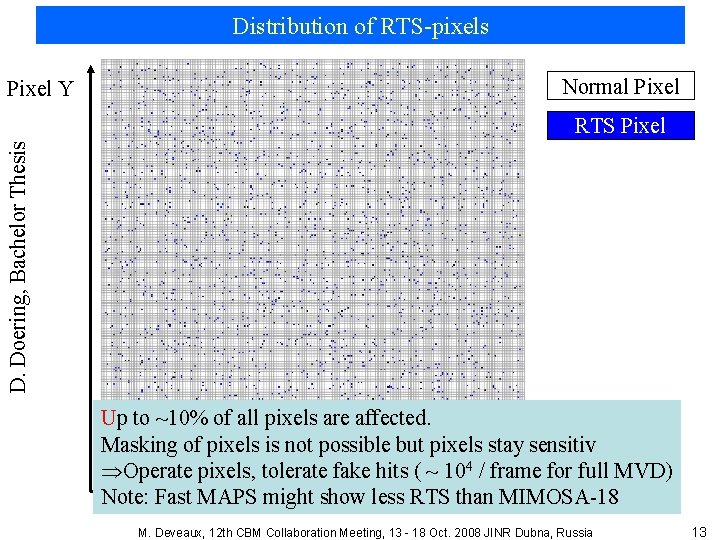
Distribution of RTS-pixels Pixel Y Normal Pixel D. Doering, Bachelor Thesis RTS Pixel Up to ~10% of all pixels are affected. Masking of pixels is not possible but pixels stay sensitiv ÞOperate pixels, tolerate fake hits ( ~ 104 / frame for full MVD) Note: Fast MAPS might show less RTS than Pixel X MIMOSA-18 M. Deveaux, 12 th CBM Collaboration Meeting, 13 - 18 Oct. 2008 JINR Dubna, Russia 13

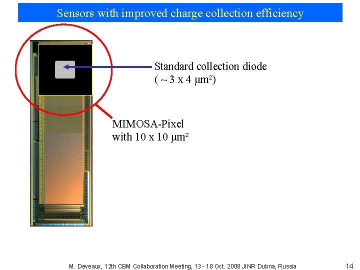
Sensors with improved charge collection efficiency Standard collection diode ( ~ 3 x 4 µm²) MIMOSA-Pixel with 10 x 10 µm² M. Deveaux, 12 th CBM Collaboration Meeting, 13 - 18 Oct. 2008 JINR Dubna, Russia 14

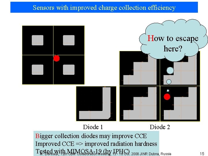
Sensors with improved charge collection efficiency How to escape here? Diode 1 Diode 2 Bigger collection diodes may improve CCE Improved CCE => improved radiation hardness Tested with (by 13 IPHC) M. Deveaux, 12 th. MIMOSA-19 CBM Collaboration Meeting, - 18 Oct. 2008 JINR Dubna, Russia 15

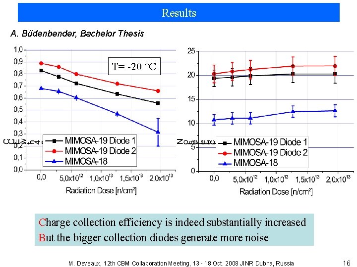
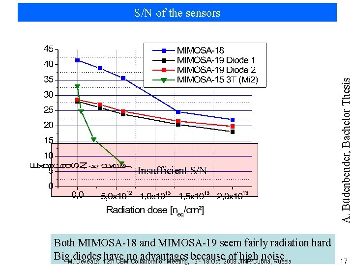
Results A. Büdenbender, Bachelor Thesis T= -20 °C Charge collection efficiency is indeed substantially increased But the bigger collection diodes generate more noise M. Deveaux, 12 th CBM Collaboration Meeting, 13 - 18 Oct. 2008 JINR Dubna, Russia 16

Insufficient S/N Both MIMOSA-18 and MIMOSA-19 seem fairly radiation hard Big. M. diodes have no advantages because of high noise Deveaux, 12 th CBM Collaboration Meeting, 13 - 18 Oct. 2008 JINR Dubna, Russia A. Büdenbender, Bachelor Thesis S/N of the sensors 17

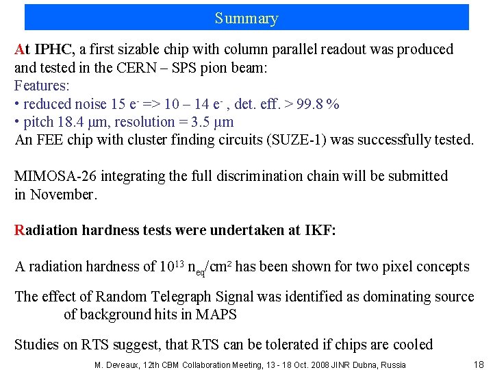
Summary At IPHC, a first sizable chip with column parallel readout was produced and tested in the CERN – SPS pion beam: Features: • reduced noise 15 e- => 10 – 14 e- , det. eff. > 99. 8 % • pitch 18. 4 μm, resolution = 3. 5 µm An FEE chip with cluster finding circuits (SUZE-1) was successfully tested. MIMOSA-26 integrating the full discrimination chain will be submitted in November. Radiation hardness tests were undertaken at IKF: A radiation hardness of 1013 neq/cm² has been shown for two pixel concepts The effect of Random Telegraph Signal was identified as dominating source of background hits in MAPS Studies on RTS suggest, that RTS can be tolerated if chips are cooled M. Deveaux, 12 th CBM Collaboration Meeting, 13 - 18 Oct. 2008 JINR Dubna, Russia 18