
Recent CMOS results and simulations Tomasz Hemperek hemperekunibonn
Recent CMOS results and simulations Tomasz Hemperek hemperek@uni-bonn. de AIDA-2020 - Marseille - 13. 05. 2016
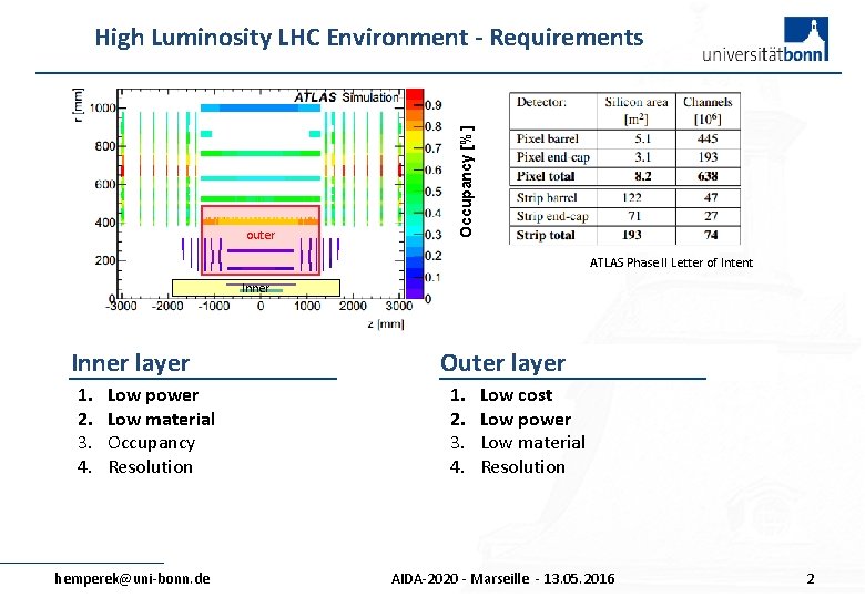
outer Occupancy [%] High Luminosity LHC Environment - Requirements ATLAS Phase II Letter of Intent Inner layer 1. 2. 3. 4. Low power Low material Occupancy Resolution hemperek@uni-bonn. de Outer layer 1. 2. 3. 4. Low cost Low power Low material Resolution AIDA-2020 - Marseille - 13. 05. 2016 2
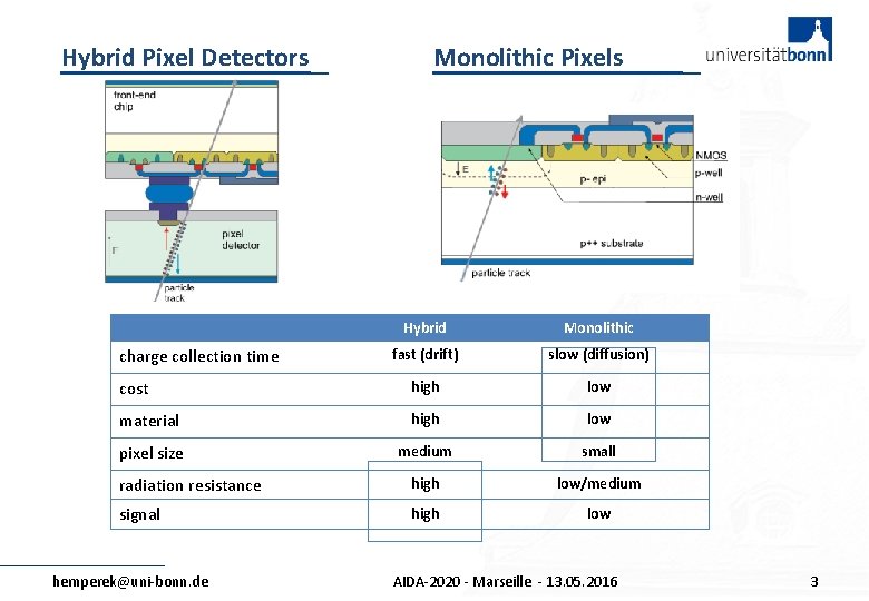
Hybrid Pixel Detectors Monolithic Pixels Hybrid Monolithic fast (drift) slow (diffusion) cost high low material high low pixel size medium small radiation resistance high low/medium signal high low charge collection time hemperek@uni-bonn. de AIDA-2020 - Marseille - 13. 05. 2016 3
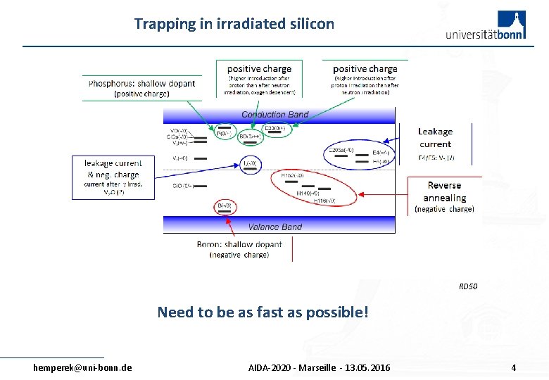
Trapping in irradiated silicon RD 50 Need to be as fast as possible! hemperek@uni-bonn. de AIDA-2020 - Marseille - 13. 05. 2016 4
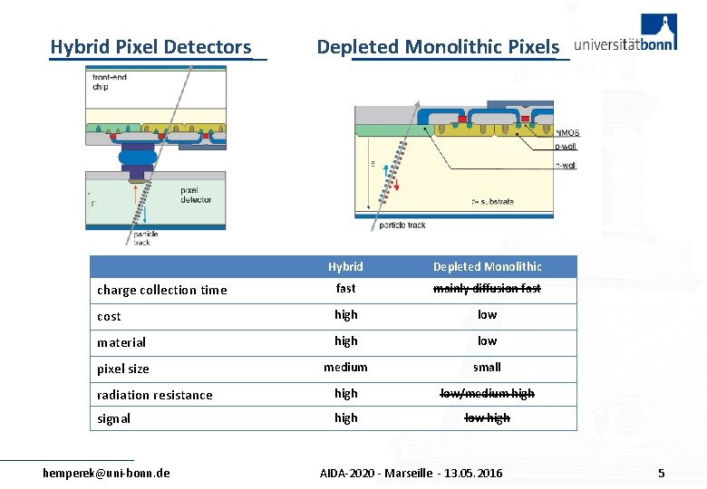
Hybrid Pixel Detectors Depleted Monolithic Pixels Hybrid Depleted Monolithic charge collection time fast mainly diffusion fast cost high low material high low pixel size medium small radiation resistance high low/medium high signal high low high hemperek@uni-bonn. de AIDA-2020 - Marseille - 13. 05. 2016 5
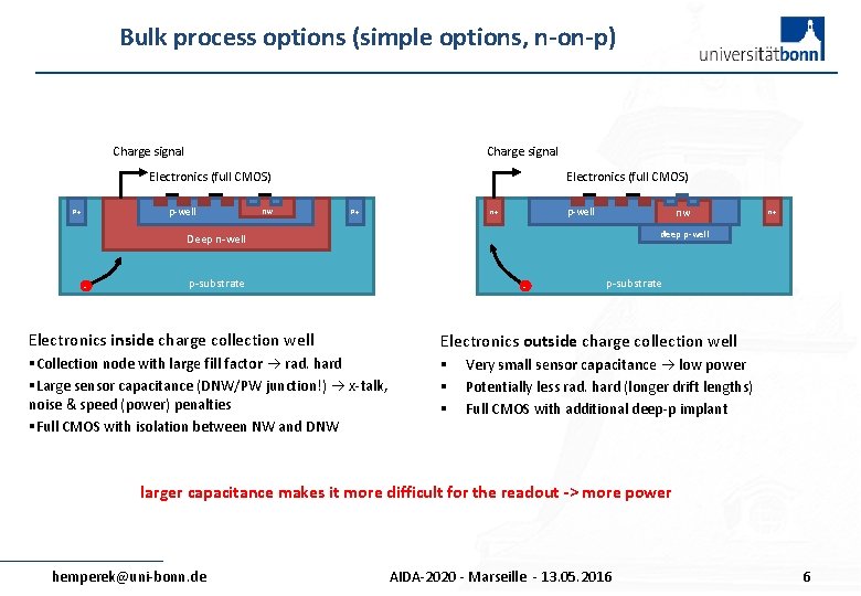
Bulk process options (simple options, n-on-p) Charge signal Electronics (full CMOS) p-well P+ nw Electronics (full CMOS) P+ p-well n+ nw deep p-well Deep n-well - n+ p-substrate - p-substrate Electronics inside charge collection well Electronics outside charge collection well §Collection node with large fill factor rad. hard §Large sensor capacitance (DNW/PW junction!) x-talk, noise & speed (power) penalties §Full CMOS with isolation between NW and DNW § § § Very small sensor capacitance low power Potentially less rad. hard (longer drift lengths) Full CMOS with additional deep-p implant larger capacitance makes it more difficult for the readout -> more power hemperek@uni-bonn. de AIDA-2020 - Marseille - 13. 05. 2016 6
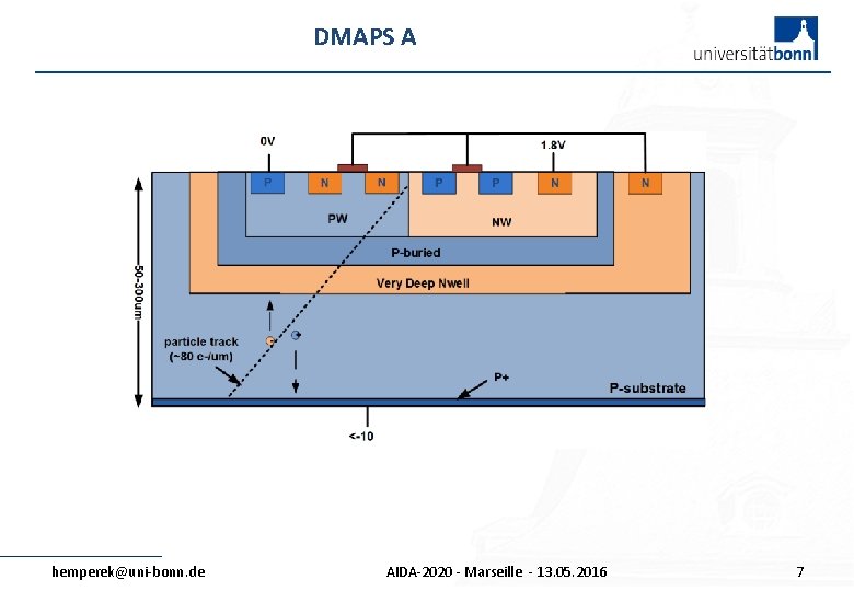
DMAPS A hemperek@uni-bonn. de AIDA-2020 - Marseille - 13. 05. 2016 7
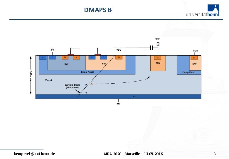
DMAPS B hemperek@uni-bonn. de AIDA-2020 - Marseille - 13. 05. 2016 8
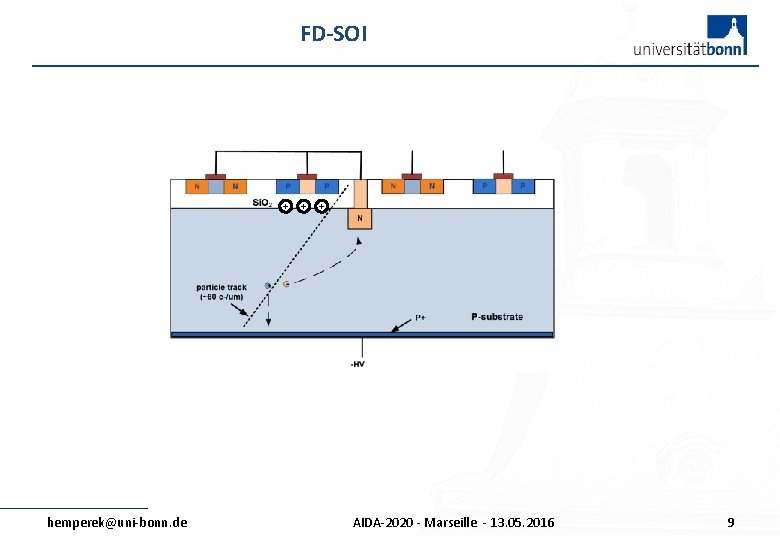
FD-SOI + + + CHANGE hemperek@uni-bonn. de AIDA-2020 - Marseille - 13. 05. 2016 9
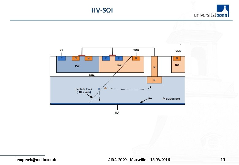
HV-SOI hemperek@uni-bonn. de AIDA-2020 - Marseille - 13. 05. 2016 10
A detail look hemperek@uni-bonn. de AIDA-2020 - Marseille - 13. 05. 2016 11
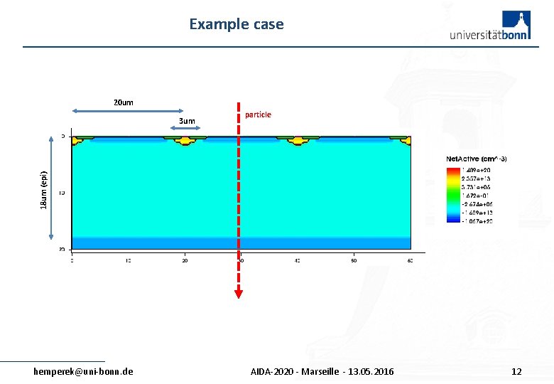
Example case 20 um particle 18 um (epi) 3 um hemperek@uni-bonn. de AIDA-2020 - Marseille - 13. 05. 2016 12
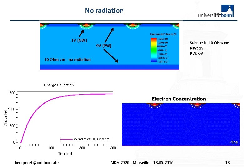
No radiation 1 V (NW) Substrate: 10 Ohm cm NW: 1 V PW: 0 V 0 V (PW) 10 Ohm cm - no radiation Electron Concentration hemperek@uni-bonn. de AIDA-2020 - Marseille - 13. 05. 2016 13
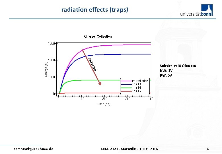
radiation effects (traps) i rad n atio Substrate: 10 Ohm cm NW: 1 V PW: 0 V no radiation hemperek@uni-bonn. de 1014 neq/cm 2 AIDA-2020 - Marseille - 13. 05. 2016 14
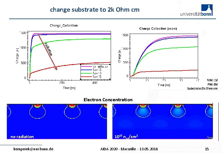
change substrate to 2 k Ohm cm n atio i rad NW: 1 V PW: 0 V Substrate: 2 k Ohm cm Electron Concentration no radiation hemperek@uni-bonn. de 1015 neq/cm 2 AIDA-2020 - Marseille - 13. 05. 2016 15
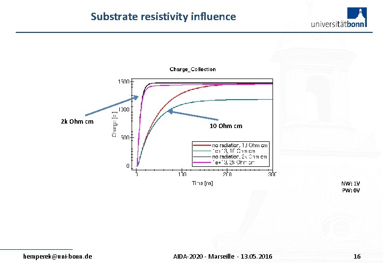
Substrate resistivity influence 2 k Ohm cm 10 Ohm cm NW: 1 V PW: 0 V hemperek@uni-bonn. de AIDA-2020 - Marseille - 13. 05. 2016 16
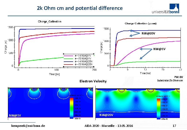
2 k Ohm cm and potential difference NW@20 V NW@1 V NW@20 V Electron Velocity NW@1 V hemperek@uni-bonn. de NW@1 V PW: 0 V Substrate: 2 k Ohm cm NW@20 V AIDA-2020 - Marseille - 13. 05. 2016 17
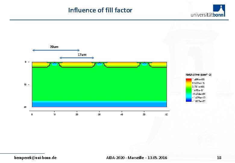
Influence of fill factor 20 um 17 um hemperek@uni-bonn. de AIDA-2020 - Marseille - 13. 05. 2016 18
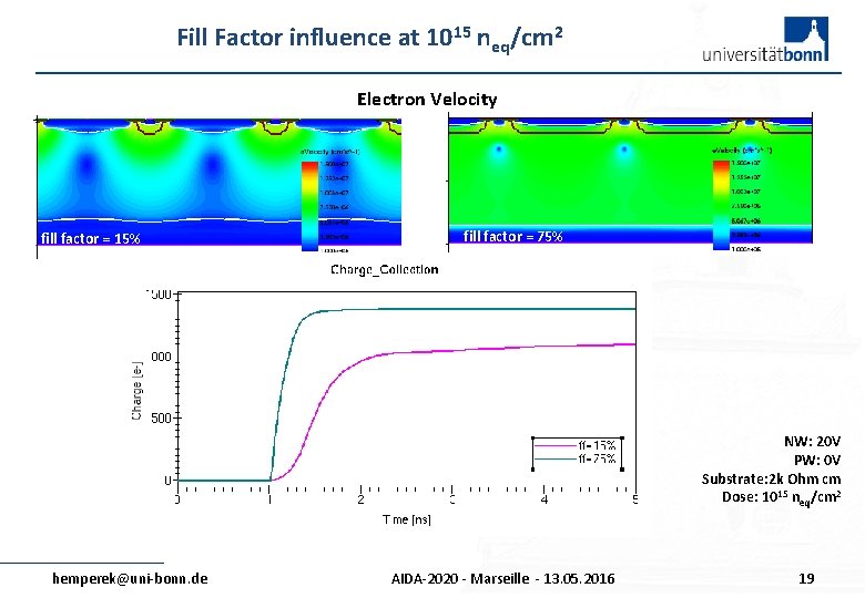
Fill Factor influence at 1015 neq/cm 2 Electron Velocity fill factor = 15% fill factor = 75% NW: 20 V PW: 0 V Substrate: 2 k Ohm cm Dose: 1015 neq/cm 2 hemperek@uni-bonn. de AIDA-2020 - Marseille - 13. 05. 2016 19
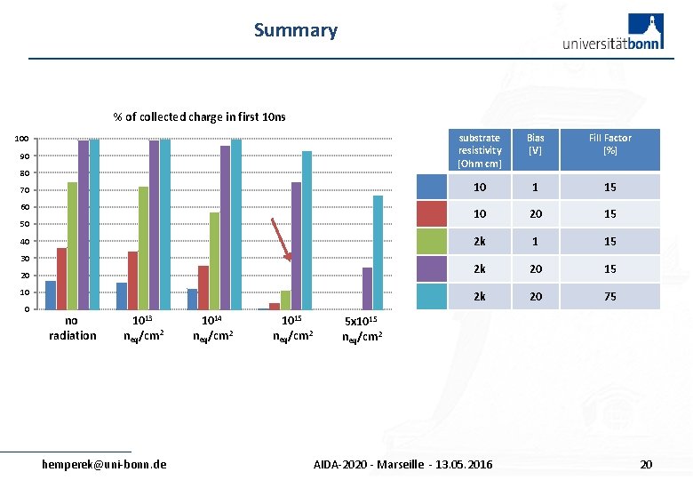
Summary % of collected charge in first 10 ns 100 90 80 70 60 50 40 30 20 10 0 no radiation 1013 neq/cm 2 hemperek@uni-bonn. de 1014 neq/cm 2 1015 neq/cm 2 substrate resistivity [Ohm cm] Bias [V] Fill Factor [%] 10 1 15 10 20 15 2 k 1 15 2 k 20 75 5 x 10¹⁵ neq/cm 2 AIDA-2020 - Marseille - 13. 05. 2016 20
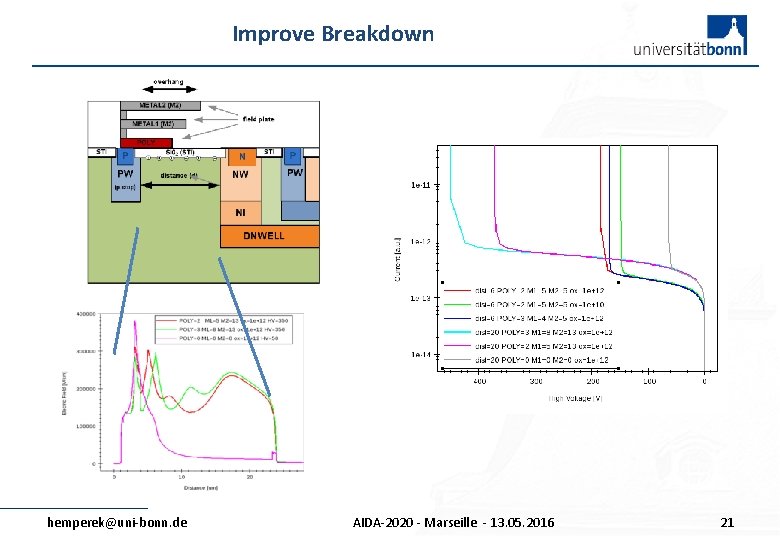
Improve Breakdown hemperek@uni-bonn. de AIDA-2020 - Marseille - 13. 05. 2016 21
Implementation hemperek@uni-bonn. de AIDA-2020 - Marseille - 13. 05. 2016 22
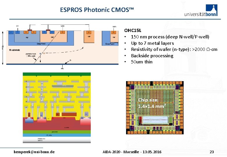
ESPROS Photonic CMOS™ OHC 15 L • 150 nm process (deep N-well/P-well) • Up to 7 metal layers • Resistivity of wafer (n-type): >2000 Ω·cm • Backside processing • 50 um thin Chip size: 1. 4× 1. 4 mm 2 hemperek@uni-bonn. de AIDA-2020 - Marseille - 13. 05. 2016 23
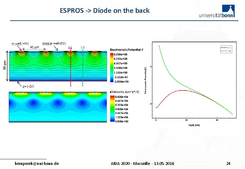
ESPROS -> Diode on the back hemperek@uni-bonn. de AIDA-2020 - Marseille - 13. 05. 2016 24
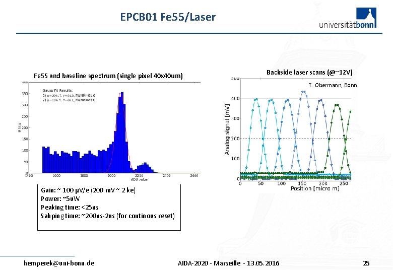
EPCB 01 Fe 55/Laser Fe 55 and baseline spectrum (single pixel 40 x 40 um) Backside laser scans (@~12 V) T. Obermann, Bonn Gain: ~ 100 µV/e (200 m. V ~ 2 ke) Power: ~5 u. W Peaking time: <25 ns Sahping time: ~200 ns-2 us (for continous reset) hemperek@uni-bonn. de AIDA-2020 - Marseille - 13. 05. 2016 25
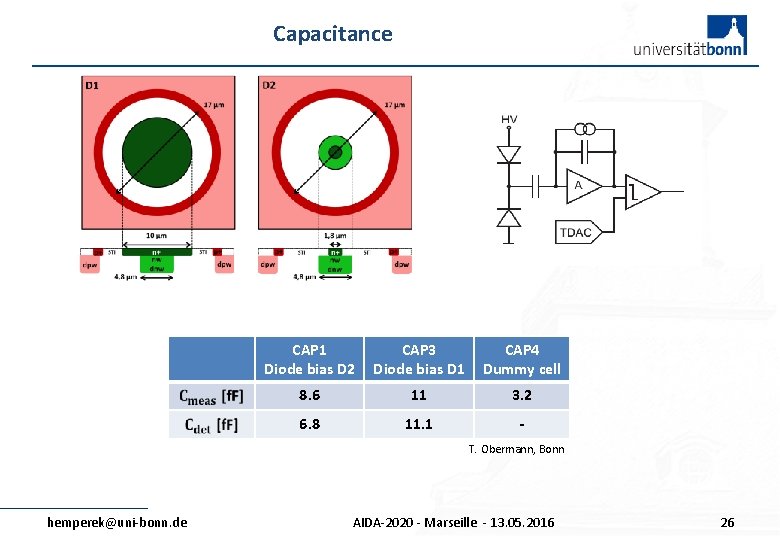
Capacitance CAP 1 Diode bias D 2 CAP 3 Diode bias D 1 CAP 4 Dummy cell 8. 6 11 3. 2 6. 8 11. 1 T. Obermann, Bonn hemperek@uni-bonn. de AIDA-2020 - Marseille - 13. 05. 2016 26
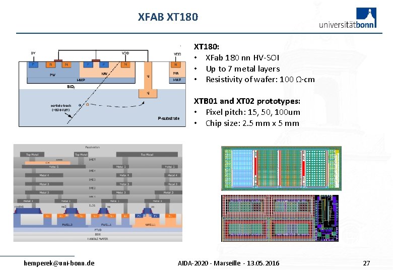
XFAB XT 180: • XFab 180 nn HV-SOI • Up to 7 metal layers • Resistivity of wafer: 100 Ω·cm XTB 01 and XT 02 prototypes: • Pixel pitch: 15, 50, 100 um • Chip size: 2. 5 mm x 5 mm hemperek@uni-bonn. de AIDA-2020 - Marseille - 13. 05. 2016 27
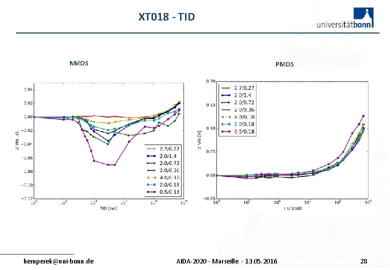
XT 018 - TID NMOS hemperek@uni-bonn. de PMOS AIDA-2020 - Marseille - 13. 05. 2016 28
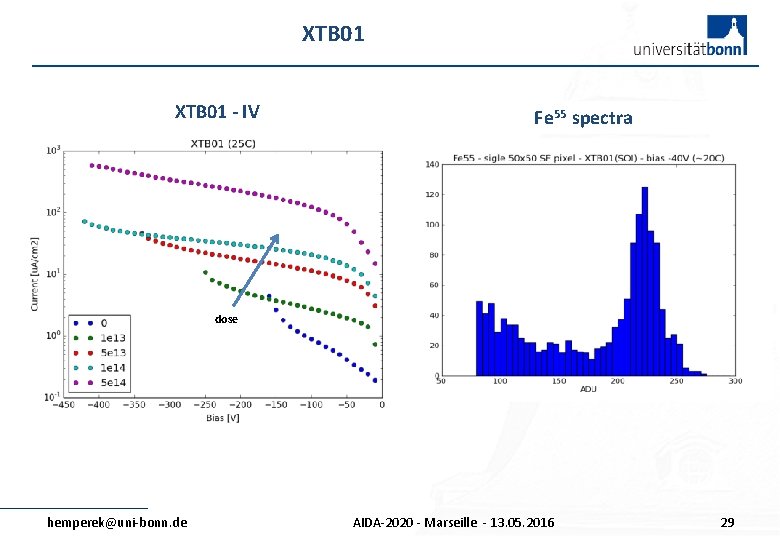
XTB 01 - IV Fe 55 spectra dose hemperek@uni-bonn. de AIDA-2020 - Marseille - 13. 05. 2016 29
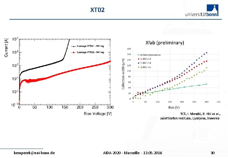
XT 02 TCT, I. Mandić, B. Hiti et al. , Jožef Stefan Institute, Ljubljana, Slovenia hemperek@uni-bonn. de AIDA-2020 - Marseille - 13. 05. 2016 30
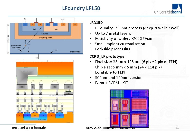
LFoundry LF 150 LFA 150: • L-Foundry 150 nm process (deep N-well/P-well) • Up to 7 metal layers • Resistivity of wafer: >2000 Ω·cm • Small implant customization • Backside processing CCPD_LF prototype: • Pixel size: 33 um x 125 um (6 pix =2 pix of FEI 4) • Chip size: 5 mm x 5 mm (24 x 114 pix) • Bondable to FEI 4 • 300 um and 100 um version • Bonn + CCPM +KIT hemperek@uni-bonn. de AIDA-2020 - Marseille - 13. 05. 2016 31
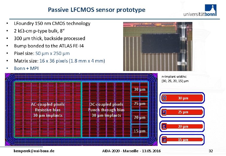
Passive LFCMOS sensor prototype n-implant widths: [30, 25, 20, 15] µm 30 µm AC-coupled pixels Resistive bias 30 µm implants DC-coupled pixels Punch through bias 30 µm implants 25 µm 20 µm 15 µm 30 µm 25 µm 20 µm 15 µm hemperek@uni-bonn. de AIDA-2020 - Marseille - 13. 05. 2016 32
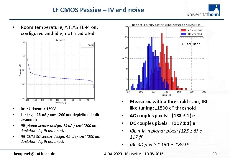
LF CMOS Passive – IV and noise • Room temperature, ATLAS FE-I 4 on, configured and idle, not irradiated D. Pohl, Bonn • • • Break down: > 160 V Leakage: 28 u. A / cm³ (200 um depletion depth assumed) IBL planar sensor design: 15 u. A / cm³ (200 um depletion depth assumed) IBL CNM 3 D sensor design: 45 u. A / cm³ (230 um depletion depth assumed) hemperek@uni-bonn. de • • Measured with a threshold scan, IBL like tuning: „ 1500 e“ threshold AC couples pixels: (133 ± 1) e DC couples pixels: (117 ± 1) e IBL n-in-n planar pixel: (125 ± 5) e, 117 f. F IBL 3 D pixel: ~ 150 e, 180 f. F AIDA-2020 - Marseille - 13. 05. 2016 33
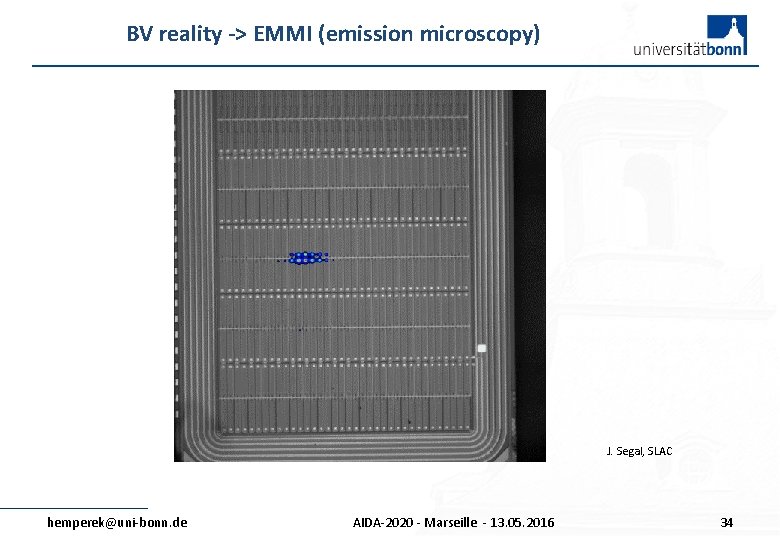
BV reality -> EMMI (emission microscopy) J. Segal, SLAC hemperek@uni-bonn. de AIDA-2020 - Marseille - 13. 05. 2016 34
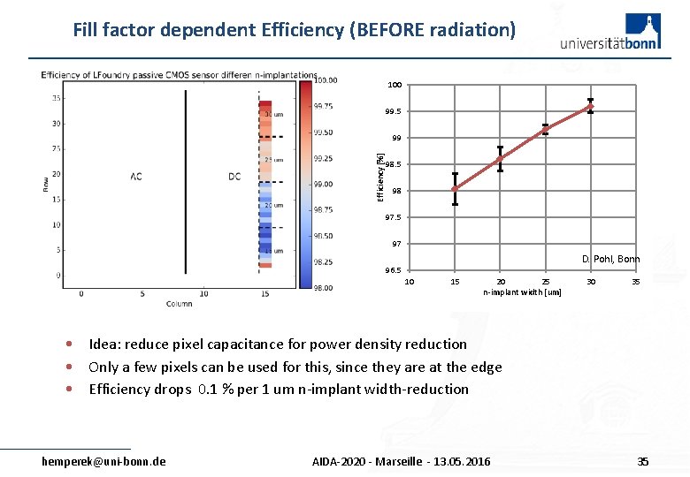
Fill factor dependent Efficiency (BEFORE radiation) 100 99. 5 Efficiency [%] 99 98. 5 98 97. 5 97 D. Pohl, Bonn 96. 5 10 15 20 25 n-implant width [um] 30 35 • Idea: reduce pixel capacitance for power density reduction • Only a few pixels can be used for this, since they are at the edge • Efficiency drops 0. 1 % per 1 um n-implant width-reduction hemperek@uni-bonn. de AIDA-2020 - Marseille - 13. 05. 2016 35
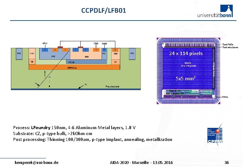
CCPDLF/LFB 01 24 x 114 pixels 5 x 5 mm 2 Process: LFoundry 150 nm, 4 -6 Aluminum Metal layers, 1. 8 V Substrate: CZ, p-type bulk, >2 k. Ohm-cm Post processing: Thinning 100/300 um, p-type implant, annealing, metallization hemperek@uni-bonn. de AIDA-2020 - Marseille - 13. 05. 2016 36
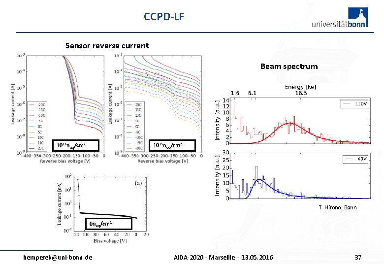
CCPD-LF Sensor reverse current Beam spectrum 1015 neq/cm 2 1013 neq/cm 2 T. Hirono, Bonn 0 neq/cm 2 hemperek@uni-bonn. de AIDA-2020 - Marseille - 13. 05. 2016 37
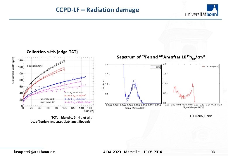
CCPD-LF – Radiation damage Collection with (edge-TCT) Sepctrum of 55 Fe and 241 Am after 1015 neq/cm 2 T. Hirono, Bonn TCT, I. Mandić, B. Hiti et al. , Jožef Stefan Institute, Ljubljana, Slovenia hemperek@uni-bonn. de AIDA-2020 - Marseille - 13. 05. 2016 38
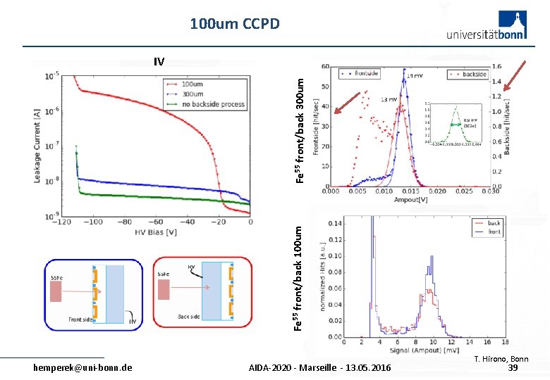
100 um CCPD Fe 55 front/back 100 um Fe 55 front/back 300 um IV hemperek@uni-bonn. de AIDA-2020 - Marseille - 13. 05. 2016 T. Hirono, Bonn 39
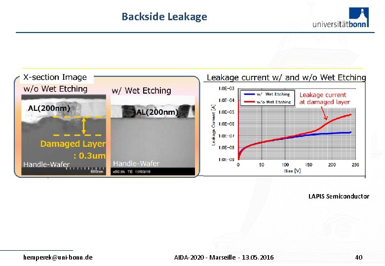
Backside Leakage LAPIS Semiconductor hemperek@uni-bonn. de AIDA-2020 - Marseille - 13. 05. 2016 40
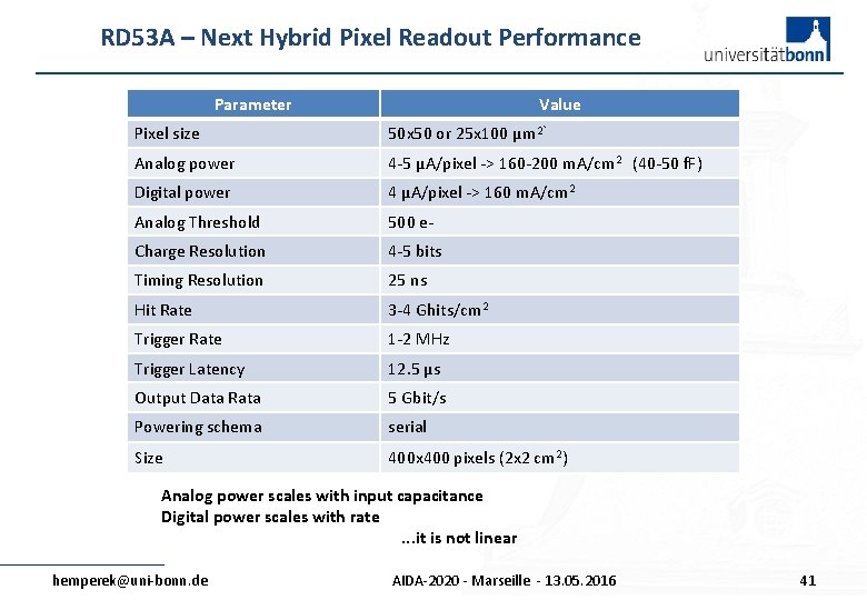
RD 53 A – Next Hybrid Pixel Readout Performance Parameter Value Pixel size 50 x 50 or 25 x 100 µm 2` Analog power 4 -5 µA/pixel -> 160 -200 m. A/cm 2 (40 -50 f. F) Digital power 4 µA/pixel -> 160 m. A/cm 2 Analog Threshold 500 e- Charge Resolution 4 -5 bits Timing Resolution 25 ns Hit Rate 3 -4 Ghits/cm 2 Trigger Rate 1 -2 MHz Trigger Latency 12. 5 µs Output Data Rata 5 Gbit/s Powering schema serial Size 400 x 400 pixels (2 x 2 cm 2) Analog power scales with input capacitance Digital power scales with rate. . . it is not linear hemperek@uni-bonn. de AIDA-2020 - Marseille - 13. 05. 2016 41

Thank you hemperek@uni-bonn. de AIDA-2020 - Marseille - 13. 05. 2016
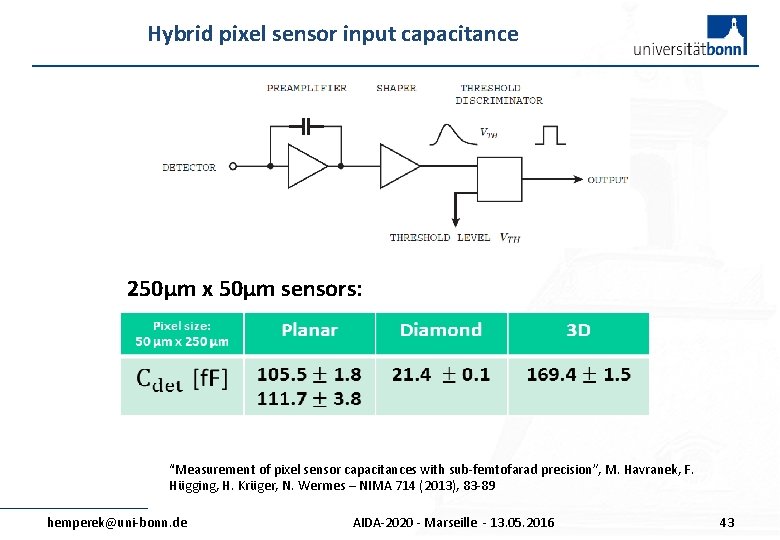
Hybrid pixel sensor input capacitance 250µm x 50µm sensors: “Measurement of pixel sensor capacitances with sub-femtofarad precision”, M. Havranek, F. Hügging, H. Krüger, N. Wermes – NIMA 714 (2013), 83 -89 hemperek@uni-bonn. de AIDA-2020 - Marseille - 13. 05. 2016 43
- Slides: 43